Note: Descriptions are shown in the official language in which they were submitted.
21100~1
-
DIGITAL SOUND LEVEL CONTROL APPARATUS
This invention relates to the main unit of a key telephone system
including a segment coder for companding (compressing and decompressing) a
5 digital audio signal, and more particularly to a sound level control apparatus for
use with an apparatus of the type described above.
Figure 1 shows a conventional monitor circuit of a digital audio
apparatus.
A conventional digital sound level control apparatus of the type
10 mentioned above includes, as disclosed in Japanese Patent Application No.
72457/1986, entitled "Monitor Circuit" shown in Figure 1, a circuit for adjusting a
sound output level by sending a code signal to a monitor section 52 from a soundlevel adjusting switch 54 and multiplying a pulse code modulation (PCM) audio
signal output from a monitor signal extraction circuit 58 by the code signal to
15 define the monitor sound level through a sound level conversion memory 57, a
digital audio convertor 56, and an analog amplifier 55.
The conventional digital sound level control apparatus includes a ROM
in which a predetermined conversion table is stored. Accordingly, the
conventional digital sound level control apparatus is disadvantageous in that
20 much labor and time are required to write the conversion table into the ROM
upon assembly of a digital key telephone system and in that, once the ROM is
incorporated into a telephone apparatus, the sound level cannot be varied in
conformity with a circuit with which the telephone apparatus is used.
It is therefore an object of the present invention to provide a digital
25 sound level control apparatus which eliminates the setting of a contrast table
between sound levels and conversion codes into a ROM.
According to a first embodiment of the invention, there is provided a
digital sound level control apparatus for the main unit of a digital key telephone
system, the main unit including a circuit control section for each telephone circuit,
30 a PCM conversion section having a segment coder for compressing with a ,u-LawPCM characteristic for each telephone circuit, a main control section for
designating a pad multiplier which defines an attenuation value corresponding to
A - 1 - ~
0 3 1
the employed telephone circuit, a digital sound level control apparatus for eachtelephone circuit and digital time switching means for switching speech paths, the
digital sound level control apparatus comprising:
means for decompressing a received ,u-Law digital PCM signal,
means for multiplying the decompressed digital signal by said
designated pad multiplier,
means for compressing the multiplied value to a ,u-Law PCM digital
signal, and
means for outputting the,u-Law digital PCM signal to the digital time
switching means.
According to a second embodiment of the invention, a digital sound
level control apparatus is provided for the main unit of a digital key telephonesystem, the main unit including a circuit control section for each telephone circuit,
a PCM conversion section having a segment coder for compressing with a ,u-Law
PCM characteristic for each telephone circuit, a main control section for
designating a pad multiplier which defines an attenuation value corresponding tothe employed telephone circuit, a digital sound level control apparatus for eachtelephone circuit and digital time switching means for switching speech paths, the
digital sound level control apparatus comprising:
first discrimination means for discriminating a segment region of a,u-
Law PCM conversion characteristic polygonal line from a segment region signal
of a PCM input data signal which is outputted from the PCM conversion section,
the PCM input data including a polarity signal, a segment region signal and a
step signal;
first calculation means for calculating a first level signal which is a data
value before compression using the output signal of the first segment region
discrimination means and the step signal of the PCM input data signal;
multiplication means for multiplying a pad multiplier by the first level
signal to output a second level signal;
second segment region discrimination means for discriminating a
segment region by comparing the second level signal with the coding threshold
- 2 -
2110031
-
values of segment regions based on the segment compression and
decompression characteristic;
second calculation means for calculating a step signal based on the
second level signal, the coding threshold signal and the intrinsic variation amount
5 per step of the segment region;
register means for forming a ~-Law PCM digital signal by combining
the original polarity signal, the calculated segment region signal and the
calculated step signal.
The first level signal of the digital sound level control apparatus
10 described above may be obtained by adding the product of the intrinsic variation
amount per step of a segment region and the step signal to the basic
normalization level signal of said segment region, or by adding the product of the
intrinsic variation amount per step of a segment region and the step signal to the
coding threshold value of said segment region.
Embodiments of the invention will now be described, by way of
example, with reference to the accompanying drawings, wherein:
Figure 1 is a block diagram of a monitor circuit of a conventional digital
sound level control apparatus;
Figure 2 is a block diagram of an embodiment of the main unit of a key
telephone system; and
Figure 3 is a block diagram of pad conversion section 13 shown in
Figure 2.
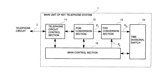
With reference to Figures 2 and 3, the main unit of key telephone
system 1 comprises circuit control section 11, PCM conversion section 12, main
control section 15, pad conversion section 13 and time divisional switch 14.
The present invention is incorporated into pad conversion section 13
and main control section 15.
Circuit control section 11 serves as an interface to telephone circuit 2
and reports to main control section 15 the classification of telephone circuits
employed for incoming telephone calls. PCM conversion section 12 converts an
incoming analog data signal into a ,u-Law PCM digital signal. Pad conversion
section 13 outputs data signal Do which is modified from PCM input data signal
..... ,,~
2110031
-
Dl from PCM conversion section 12 to digital data having a controlled sound level
by decompressing, multiplying by pad multiplier Pd sent from main control section
15 and compressing to ,u-Law PCM digital data. Main control section 15 outputs
multiplier Pd signal to pad conversion section 13 corresponding to the employed
5 incoming telephone circuit by discriminating by notification from circuit control
section 11. Time divisional switch 14 switches telephone calls by switching the
connection of the PCM highway.
PCM input data signal Dl is an 8-bit signal wherein the MSB
corresponding to the eighth bit serves as polarity signal P, the three bits
10 corresponding to the seventh to fifth bits serve as a segment region (referred to
as region signal A hereafter) which identifies a segment, and the remaining fourbits corresponding to the fourth to first bits serve as step signal bits S
representative of a position in a segment.
Region signal A includes intrinsic variation signal A1 representative of
15 the variation amount per step of the level value in the segment region beforecompression, basic normalization level signal A2 (4,191 in region 8; 2,079 in
region 7; 1,023 in region 6 and the like) representative of a reference point for
each segment region before compression, and coding threshold value A3 (4,063
in region 8; 2,015 in region 7; 991 in region 6 and the like) representative of the
20 start point of each region before compression.
Pad conversion section 13 converts compressed PCM input data into
data of the level before compression with reference to the basic normalization
level signal before compression, multiplies the data of the thus converted or
decompressed level by a pad multiplier to convert the data into a predetermined
25 sound volume, compresses the volume signal again, and outputs the thus
compressed volume signal to the time divisional switch 14. Pad conversion
section 13 includes register 31 for temporarily storing input data signal Dl,
another register 32 for temporarily storing the pad multiplier signal Pd, regiondiscrimination circuit 33 for discriminating region signal A in PCM input data
30 signal Dl and dividing region signal A into intrinsic variation signal A1,
normalization reference level signal A2 and coding threshold value A3,
multiplication circuit 34 for multiplying step signal S in PCM input data Dl by
`` 21100~1
-
intrinsic variation amount signal A1, addition circuit 35 for adding basic
normalization level signal A2 to the output signal of multiplication circuit 34 to
output level signal Ll, another multiplication circuit 36 for multiplying input level
signal Ll by pad multiplier signal Pd to produce output level signal LO, region
comparison discrimination circuit 37 for comparing output level signal LO and
coding threshold value A3 to determine to which region output level signal LO
corresponds, and outputting region signal A' based on the determination,
subtraction circuit 38 for subtracting coding threshold value A3 intrinsic to a
region determined from region signal A from output level signal LO, division
circuit 39 for dividing the output of subtraction circuit 39 by intrinsic variation
signal A1 to output step signal S', and register 40 for temporarily storing polarity
signal P, region signal A' and step signal S'.
Operation of the embodiment will now be described below.
Analog audio data received from telephone circuit 2 are inputted by
way of circuit control section 11 and converted into a PCM signal by PCM
conversion section 12. In this instance, circuit control section 11 determines
whether the received call has originated from an extension line or another
subscriber line and notifies the result of the determination to main control section
15.
Meanwhile, PCM coded audio data are outputted by PCM conversion
section 12 to pad conversion section 13 as input data signal Dl. Separately,
depending on the result of the determination of either an extension line or another
subscriber line previously notified to main control section 15, pad multiplication
value signal Pd representative of an attenuation amount is sent from main control
section 15 to pad conversion section 13, and PCM output data signal Do for
which the sound volume difference has been adjusted is outputted to time
divisional switch section 14 in which a PCM highway is exchangeably connected.
The sound level difference among calls from extension lines and other
subscriber lines can thus be eliminated by the way that multipliers to designateattenuation amounts are set and stored in main control section 15 in such a
manner that the attenuation amount is, for example, 0 dB for a call received from
outside line 2 and 6 dB for a call received from an extension line.
-5-
211~0~1
-
The operation of pad conversion section 13 of the embodiment will now
be described.
PCM input data signal Dl from PCM conversion section 12 is inputted
to 8-bit register 31 while pad multiplier value signal Pd for determination of the
5 attenuation amount from main control section 15 is inputted to 4-bit register 32.
Region discrimination circuit 33 discriminates a region from region
signal A in PCM input data signal Dl inputted to register 31 and outputs basic
normalization level signal A2 intrinsic to the region, intrinsic variation amount
signal A1 intrinsic to the region determined from region signal A, and coding
10 threshold value A3.
Multiplication circuit 34 multiplies intrinsic variation value signal A1 by
step signal (bits 4 to 1) S of PCM input signal Dl, and the product is added to
basic normalization signal A2 by addition circuit 35. The sum of the addition isoutputted as input level signal Ll. Meanwhile, polarity signal P (bit 8) of PCM
15 input data signal Dl is not inputted to region discrimination circuit 33 but is
outputted as is as a polarity signal of PCM output data signal Do.
The pad multiplication value signal Pd sent from main control section
15 is inputted to and then outputted from register 32.
Multiplication circuit 36 multiplies input level signal Ll outputted from
20 addition circuit 35 by pad multiplication value signal Pd outputted from register
32 and outputs the result of the multiplication as output level LO.
Segment region comparison discrimination circuit 37, which compares
coding threshold value A3 determined from region signal A by region
discrimination circuit 33 and output level signal Lo outputted from multiplication
25 circuit 36, determines the region to which output level signal Lo corresponds, and
outputs corresponding region signal A' (bits 7 to 5).
Further, the result of the substraction of coding threshold value A3
from output level signal LO by subtraction circuit 38 is divided by intrinsic
variation signal A1 determined from region signal A' by division circuit 39, and the
30 result of the division is outputted as step signal S' (bits 4 to 1).
PCM output data signal Do after conversion into a pad value instructed
by main control section 15 from polarity signal P (bit 8), region signal A' (bits 7
2110~31
-
to 5), and step signal S' (bits 4 to 1) is stored once into and then outputted from
register 40.
Meanwhile, main control section 15 outputs pad multiplication value Pd
to pad conversion section 13 in accordance with the type of circuit. Where the
5 number of types of circuits involved is great, it may be possible to provide means
for setting correspondence tables so that the corresponding pad multiplier may
be outputted for each of the types of circuits.
Further, while, in the present embodiment, input level Ll is obtained by
the addition of the product between intrinsic variation signal A1 and step signal
10 S to the normalization reference level signal A2, it may be obtained otherwise by
the addition of the product of the intrinsic variation amount signal A1 and the step
signal S to the coding threshold value A3.
As described above, since region signals and step signals
corresponding to the circuits from which calls are received, rather than fixed
15 region signals and step signals, as in the case of a conventional digital sound
level control apparatus, are outputted from the digital sound level control
apparatus of the invention by calculating the region signal and the step signal,there is an advantage in that the reception sound level can be held substantially
constant irrespective of the type of telephone circuit from which a call is received.
A