Note: Descriptions are shown in the official language in which they were submitted.
1- 2110149
HIGH FREQUENCY SIGNAL DETECTING CIRCUIT
BACKGROUND OF THE INVENTION
The present invention relates to a detecting circuit for dçtecting a high frequency
or radio frequency (RF) signal and, more particularly, to a detecting circuit of the type
required to have a linear detection characteristic, as one used to control tr~n~mi~.~ion power
5 in a TDMA (Time Division Multiple Access) co~ llunication system.
A detecting circuit of the type described has to meet the following two requisites
at the same time when used to detect a TDMA signal or similar RF signal whose power level
may change from one time slot to another. One requisite is that the mean detection output
level of the circuit be m~int~inPd smooth in data fields. The other requisite is that a transition
10 time existing between nearby time slots be confined in a range which does not effect the mean
detection output level. However, a detecting circuit meeting both of these requirements has
not been reported yet.
- 2 - 2 110 1~9
SUMMARY OF THE II~VENTION
It is, therefore, an object of the present invention to
provide a detecting circuit capable of smoothing mean power
in each time slot and, at the same time, performing rapid
5 response during each transition time.
A detecting circuit of the present invention comprises a
detector for detecting the envelope of a high frequency signal
whose mean power level may change depending on the time
slot, and a low-pass filter responsive to a control signal for
1 0 broadening the pass band for the output of the detector only
during the transition time of the mean power level of the high
frequency signal.
BRIEF DESCRIPTION OF THE DRAWINGS
1 5 The above and other objects, features and advantages of
the present invention will become more apparent from the
following detailed description taken ``with the accompanying
drawings in which:
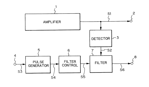
FIG. 1 is a block diagram schematically showing a
2 0 detecting circuit embodying the present invention;
FIG. 2 shows the levels of power input to a detector
included in the embodiment;
FIG. 3 shows the levels of the output of the detector;
FIGS. 4A-4C show the waveforms of signals appearing in
2 5 the embodiment;
,~
-
~ 3 ~ 21101~9
FIG. 5 is a circuit diagram showing specific
constructions of a filter and a filter control included in the
embodiment;
FIG. 6 is a schematic block diagram of a conventional
detecting circuit; and
FIG. 7 shows the output of the circuit shown in FIG. 6.
DESCRIP 1 lON OF THE PREFERRED EMBODIMENT
To better understand the present invention, a brief
1 0 reference will be made to a conventional high frequency
detecting circuit, shown in FIG. 6. As shown, the detecting
circuit includes a detector 3 connected to an amplifier 1. The
amplifier 1 is provided at the final stage of, for example, a
transmitter included in a digital mobile telephone system.
1 5 The amplifier 1 delivers a TDMA signal Sl to an output
terminal 2. The TDMA signal S 1 is an example of
transmission signals particular to dig`ital mobile telephones
now under development in Japan, as taught in the Journal of
the Institute of Electronic Data Communication Engineers of
2 0 Japan, Vol. 73, No. 8, August 1990. Specifically, in the TDMA
signal 1, three channels are accommodated in a single carrier
lying in the 800 MHz band or 1.5 GHz band, and a single frame
is made up of three time slots TS 1 -TS3 and repeated at a
period of 20 mS; each time slot TS has a duration of 6.7 mS.
2 5 The TDMA signal 1 has a data field Td in each time slot TS and
-
- 4 - 2110149
has, between nearby time slots TS, a transition time or field
Tr beginning at the end of the data field Td of the preceding
time slot TS (standardized duration being about 90 ~S). The
transition time Tr includes a guard time. The power level o f
5 the TDMA signal 1 differs from one destination to another,
i.e., from one time slot TS to another in respect of a mean
value P; the data fields Td of the time slots TS 1, TS2 and TS3
have mean values Pl, P2 and P3, respectively. Further, even
in the same data field Td, the instantaneous value changes
1 0 with the content of data (see FIG 2, portion A).
The detector 3 shown in FIG. 6 detects the envelope of
the TDMA signal 1 and produces an output S2. FIG. 3 shows
the levels of the detector output S2. Since the detector 3
lacks the function of limiting the frequency band of the input
1 5 signal, the time response of the detector output S2
corresponds to the TDMA signal S 1. In addition, the above-
mentioned mean power P and the detector output level D are
proportional to each other.
The prerequisite with a digital mobile telephone system
2 0 is that the mean value P of the power level of the TDMA signal
S 1 be controlled on a time slot TS basis. To meet this
prerequisite, the power level of each data field Td has to be
prevented from changing with the content of data. For this
purpose, a filter 61, FIG. 6, is connected to the output of the
2 5 detector 3. Specifically, the filter 61 limits the frequency
2110149
band of the detector output S2 to thereby smooth the detector
output level D in each data field Td. The resulting output S3
of the filter 61 is delivered to an output terminal 62 as a
detection output. The filter 61 is implemented as an active
5 filter.
The detection output S3 eliminates the changes in the
detector output level D ascribable to changes in data.
However, the signal S3 increases the transition time Tr to t h e
next time slot TS. Specifically, as shown in FIG. 7, the levels
10 D 1 and D2 of the detector output S2 in the time slots TS 1 and
TS2 are different from each other. As a result, the transition
from the level D 1 to the level D2 needs a transition time Tr2
longer than the transition time Tr. Moreover, the transition
times Trl, Tr2 and Tr3 associated with the time slots TS 1,
1 5 TS2 and TS3 are different from each other. Since the
transition times Tr 1 -Tr3 each extends into the associated
data field Td, the mean level D of the- detection output S3 is
effected, in the data field Td where the detector output level
D should remain constant, by the detector output level of t h e
2 0 preceding time slot TS. This requires, for example, the data
at the detector output level D to be discarded in part of the
data field Td. In this manner, the conventional detecting
circuit suffers from various limitations in producing an
accurate output S3 in each time slot TS.
r
- 6 - 2110 149
More specifically, the filter 61 smooths the data f i e 1 d s
Td of the detector output S2 and, therefore, does not change
the cut-off frequency. In this condition, if a low cut-off
frequency is selected, the time constant of the filter 61 will
5 increase and cause the period of time necessary for the
transition time Tr to be processed to increase. This causes
the transition time Tr to extend into the data field Td of t h e
detector output S2~ thereby reducing the period of time
available for sampling the data field Td. Consequently, the
10 number of data to be sampled in the data field Td is reduced,
forcing a part of the data field Td to be discarded.
As stated above, in the event of detecting a TDMA signal
or similar RF signal whose power level may change from one
time slot to another, the conventiona] detecting circuit
1 5 cannot confine the transition time between nearby time slots
in a range which does not effect the mean output level, while
maintaining the output level smooth irt the data field.
Referring to FIG. 1, a detecting circuit embodying the
present invention is shown. As shown, the detecting circuit
2 0 has a control signal input terminal 4, a pulse generator 5, a
filter control 6, a filter 7, and an output terminal 8, in
addition to the conventional amplifier 1, detector 3, and
output terminal 2. As shown in FIG. 4A, a control signal S3
has a pulse width of 20 ~S and a period of time slots TS. The
2 5 control signal S3 comes in through the input terminal 4 at
.
- 7 - 21 10 1~ 9
times Tl, T2 and T3 in synchronism with the beginnings of
consecutive transition times Tr. The pulse generator 5
generates a pulse signal S4, FIG. 4B, having the same duration
(pulse width of 90 ~S) as the transition time Tr every time
5 the control signal S3 arrives. The pulse signal S4 is applied
to the filter control 6.
The filter 7 is implemented as a low-pass filter for
limiting the frequency band of the output S2 of the detector 3.
Specifically, the filter 7 changes the pass band of the
10 detector output S2, i.e., the cut-off frequency fc under the
control of the filter control 6. More specifically, when the
pulse signal S4 is in a high level (transition time Tr), the
filter 7 forms a broad pass band, i.e., raises the cut-off
frequency. As a result, a detection output with rapid
1 5 response, as shown in FIG. 4C, is fed to the output terminal 8.
On the other hand, when the pulse signal S4 is in a low level
(data field Td), the filter 7 forms a- narrow pass band, i.e.,
lowers the cut-off frequency. Consequently, a detection
output S6, FIG. 4C, having a smoothed response is fed out v i a
2 0 the output terminal 8. In this manner, in each data field Td of
the TDMA signal Sl, the detection output S6 has the level F
thereof smoothed and maintained constant without regard to
the content of data. At the same time, in each transition
field Tr, the output level F follows a change in the p o w e r
,~
- 8 - 2 110 1~9
level of the TDMA signal Sl immediately since the filter 7
responds at high speed.
Specific circuitry including the filter 7 and filter
control 6 is shown in FIG. 5. The filter 7 is an active filter.
As shown, the output S2 of the detector 3 is applied to an
input terminal 71 included in the filter 7. The signal S2 is
routed through resistors 72 and 74 having the same
resistance R to the non-inverting input of an operational
amplifier 76. The operational amplifier 76 has the non-
10 inverting input thereof connected to ground via a capacitor 75whose capacitance is C2. The output terminal of the
amplifier 76 is connected to an output terminal 77 on which
the detection output S6 appears. The detection output S6 is
fed back to the inverting input of the amplifier 76 directly
1 5 and via a capacitor 73 having a capacitance Cl and the
resistor 74. The cut-off frequency fc of the filter 7 is
expressed as:
fc = lI2~ T C1 R
2 0
The filter control 6 is implemented by a switch 60
which is turned on and turned off by the pulse signal S4
applied thereto from the pulse generator 5. The switch 60
may be implemented by an IC (Integrated Circuit), e.g.,
2 5 !1PD4538 available from NEC Corporation. When the pulse
-
9 21101~9
signal S4 is in a high level, the switch 60 short-circuits t h e
resistors 72 and 74 of the filter 7. Specifically, since the
resistors 72 and 74 are not connected, the time constant of
the filter 7 decreases. The capacitor 73 discharges when the
5 data field Td changes from a high level to a low level or
charges when the data field Td changes from a low level to a
high level. This is successful in reducing the transmission
time Tr to less than 90 ,uS and, therefore, in guaranteeing a
sufficient sampling time. On the other hand, when the pulse
1 0 signal S4 is in a low level, the switch 60 does not short-
circuit the resistors 72 and 74 of the filter 7. At this time,
the conventional smoothing operation is effected, and the
filter 7 restores the greater time constant. As a result, when
the pulse signal S4 is in a low leve3, the filter 7 produces a
1 5 detection output S6 having the cut-off frequency represented
by the above equation and frequency components of 0 to fc.
Since one time slot is 6.7 mS long and the transition time Tr
is 90 ,uS, the cut-off frequency fc should preferably be about
3 kHz. On the other hand, when the pulse signal S4 is in a high
2 0 level, the cut-off frequency of the filter 7 is determined by
the cut-off frequency fca of the operational amplifier 7 6
since the resistors 74 and 72 are short-circuited.
Considering the transition time Tr which is 90 ~lS, the cut-off
frequency fca will respond to the transition time T r
2 5 sufficiently if it is higher than 30 kHz.
2110149
1 o -
It is to be noted that the control signal S3 applied to t h e
pulse generator 5 is generated by a control signal generator 9,
FIG. 5, in synchronism with a host station.
In summary, in accordance with the present invention, a
5 detecting circuit has a detector for detecting the envelope of
an RF signal whose power level may change depending on the
time slot, and a filter for narrowing the pass band in the data
field of each time slot and broadening it in the transition
field of the same. The output of the detector is applied to the
1 0 filter. The detecting circuit, therefore, produces an output
which is smoothed in the data field without regard to the
content of data and which responds to a change in the power
level sharply in the transition field.
Various modifications will become possible for those
1 5 skilled in the art after receiving the teachings of the present
disclosure without departing from the scope thereof.