Note: Descriptions are shown in the official language in which they were submitted.
Description
Methods of Fabricating Dual Anode, Flat
Panel Electrophoretic Displays
Technical Field
The present invention relates to electrophoretic
display apparatus in general and more particularly to
methods for fabricating such displays having a dual anode
structure.
Background Art
A dual anode, flat panel, electrophoretic display
apparatus has been described in copending application Serial
No. 2,012,711 filed March 21, 1990 entitled Dual Anode Flat
Panel Electrophoretic Display Apparatus for Frank J. DiSanto
and Denis A. Krusos, the inventors herein and assigned to
Copytele Inc., the assignee herein (issued to patent on July
16, 1996). That application describes an electrophoretic
display which has a grid cathode matrix arrangement
consisting of a first plurality of conductive lines which
are transverse to said first plurality. Located with
respect to the grid and cathode are first and second anode
structures. The first anode is removed from the second with
the second anode overlying the grid lines of the display and
insulated therefrom. The second anode is biased to
implement typical hold and erase modes independent of the
first anode and the display structure as indicated in the
application exhibits many advantages when compared with
prior art displays.
The electrophoretic display (EPID) is well known
and there exists many patents and articles in the prior art
which describe operation and characteristics as well as
describing methods of fabricating such displays. The
following patents are illustrative of
WO 92/21733 ~ ~ ~ O 2 9 ~ PCT/US91/03759
_2_ .,
prior art devices and approaches. These patents
issued in the name of Frank J. DiSanto and Denis A.
Krusos, the inventors herein. Apart from the patents
to be described below, there are of course many
references which were cited in the prosecution of
these patents as well as additional references which
were cited in the background of these patents. Many
of the techniques and methods of fabricating such
displays are disclosed in the patents that follow, as
well as in the additional references as indicated. ,
U.S. Patent 4,655,897 issued on April 7, 1987
entitled Electrophoretic Display Panels and Associated
Methods describes a typical electrophoretic display
apparatus utilizing an X-Y matrix consisting of grid
and cathode lines which are insulated one from the
other and which are associated with an anode
electrode. The space between the grid and cathode
lines and the anode electrode is filled with an
electrophoretic dispersion. The patent describes
techniques for making such displays as well as
suitable dispersions and materials for use with such
displays.
U.S. Patent No. 4,732,830 issued on March 22,
1988 entitled Electrophoretic Display Panels and
Associated Methods describes methods for making
electrophoretic displays as well as describing display
construction and operation.
U.S. Patent No. 4,742,345 issued on May 3, 1988
entitled Electrophoretic Display Panel Apparatus and
Methods Therefore describes improved electrophoretic
display panels exhibiting improved alignment and
contrast as well as describing circuitry for use with
such a display and methods for fabricating such a
display.
WO 92/2l733 PGT/US91/03759
_ ~~.~.~~~~'~
U.S. Patent No. 4,746,917 issued on May 24, 1988
entitled Method and Apparatus for Operating
Electrophoretic Displays Between a Display and a Non-
Display Mode describes various biasing techniques for
operating electrophoretic displays to provide writing,
erasing as well as operating the display during a
display and non-display mode.
U.S. Patent No. 4,722,820 issued on September 20,
1988 entitled Monolithic Flat Panel Display Apparatus
describes methods and apparatus for fabricating flat ,
panel displays employing electrophoretic principles as
well structures to enable such displays to be biased
and driven by additional circuitry.
Thus, as one can see, an important consideration
of the prior art is to provide an improved display
with increased contrast, faster operating time, and
more reliable performance. As indicated in the above
noted copending application, a particularly disturbing
problem which occurs in electrophoretic displays
results in the appearance of a bright "flash"
emanating from the display during the ERASE mode.
This "flash" while occurring over a relatively short
period is perfectly visible. The "flash" appears
disturbing to many individuals who view the display
and is caused by the following phenomenon. For proper
operation of the electrophoretic display, the amount
of pigment in the suspension is considerably greater
than the pigment required to give a suitable
background when the panel is in a HOLD condition. The
term HOLD is well known in the art, and the
electrophoretic panel is placed in a HOLD condition
prior to writing the display. In this manner the HOLD
condition is achieved when the anode is at a high
WO 92/2l733 PCT/US91/03759
positive voltage, the grid is at a low voltage, and
the cathode is at a high voltage.
Typically, the anode would be at a voltage for
example of 200 volts with the grid at a lower voltage
as for example -12 volts with the cathode at a high
voltage which would be +15 volts. With these voltages
on the typical prior art electrophoretic display, the
display is in the so-called HOLD condition. This HOLD
condition is implemented prior to the WRITE mode
during which mode new information is written into the ,
display. The excess pigment during the HOLD condition
is at the surface of the anode which is at the highest
potential with respect to any other of the electrodes.
To ERASE the display, the anode is made negative and
all the pigment leaves the anode and is at the surface
of the grid and cathode. During ERASE, the anode, for
example, would be placed at -200 volts. Hence, during
the ERASE mode, a11 the pigment leaves the anode and
is now at the surface of the grid and cathode
accordingly. The cathode side of the flat display
during the ERASE mode is considerably brighter than it
is during the HOLD causing a bright "flash" to appear
on the display even when the ERASE time is extremely
short.
The "flash" occurs between frames and may exist
every 20 to 30 milliseconds caused by the change in
brightness between the HOLD and the ERASE mode. It
is, of course, desirable to eliminate this bright
"flash" so that the display appears more uniform and
stable.
Hence, the above-noted copending application
describes the addition of a second anode which is
interposed between the original anode of the
electrophoretic display and the cathode-to-grid
matrix. The second anode aides in preventing this flash by
allowing the pigment to be selectively controlled.
This present application describes methods for
fabricating a dual anode display. The methods to be
described show a second anode or an additional anode which
in one embodiment is designed to be parallel with the grid
structure and in another embodiment is transverse or
perpendicular to the grid structure. These methods include
the selective deposition of different materials such as
metals and insulators together with the use of selective
etches in order to achieve the desired results.
According the a broad aspect of the present
invention there is provided a method of completing
fabrication of an electro-phoretic display after a plurality
of cathode conductor lines indicative of an X matrix have
been formed on planar glass sheet. The method comprises:
coating the cathode conductor lines with a
first insulating layer of photoresist;
coating the first insulating layer with a
first layer of silicon dioxide;
coating a first layer of metal on said layer
of silicon dioxide;
coating said first layer of metal with a
second layer of photoresist;
coating said second layer of photoresist with
a second layer of silicon dioxide;
coating said second layer of silicon dioxide
with a second layer of metal capable of being etched by a
different etchant than said first;
coating said second layer of metal with a
third layer of metal capable of being etched by a different
etchant from said first and second layer of metal;
coating said third layer of metal with a
fourth layer of metal capable of being etched by a different
etchant than said first, second and third layers of metal,
- 5A -
coating said fourth layer of metal with a
third layer of photoresist;
treating said fourth layer of photoresist to
photolitho-graphically form a matrix of lines transverse to
said cathode conductor lines and thereafter selectively
etching each layer of material until channels separate each
of the lines of said matrix wherein there are first and
second metal structures insulated from each other and from
the cathode structure;
coating the treated structure with a layer of
silicon dioxide;
removing said layer of silicon dioxide as
coating said fourth metal layer with said fourth metal
layer.
According to a still further broad aspect the
method comprises the steps of:
depositing a first thin layer of a conductive metal on a
carrier plate of glass;
etching said layer to form a line pattern
indicative of an X cathode matrix;
depositing a first insulating layer of a
photoresist resin on said X cathode matrix;
depositing a first layer of silicon dioxide
on said first layer of photoresist resin;
depositing a second layer of a conductive
metal on said layer of silicon dioxide;
depositing a second insulating layer of a
photoresist resin on said second metal layer;
exposing said second layer of photoresist
with a Y grid matrix mask;
developing said photoresist according to said
Y grid mask;
etching said second layer of said conductive
metal to form said Y grid matrix;
;:
- 5B -
removing the remainder of said second layer
of photoresist;
etching said layer of silicon dioxide with
said etched second layer of conductive metal serving as a
mask;
depositing a third layer of photoresist resin
on said etched second layer;
depositing a second layer of silicon dioxide
on said third layer of photoresist;
depositing a first anode metal layer on said
layer of silicon dioxide;
depositing a second different anode metal
layer on said first anode metal layer;
depositing a fourth layer of a photoresist
resin on said second different metal layer;
treating said fourth layer of photoresist to
photolitho-graphically form an anode matrix of lines
parallel to said Y grid matrix and perpendicular to said X
cathode matrix;
etching said first and second anode layers;
covering said structure with a thin layer of
silicon dioxide and etching away said second layer of anode
metal leaving said first anode layer to provide an
additional matrix designated as an anode matrix for said
display.
-
Fig. 1 is a partial cross-sectional view showing
an electrophoretic display useful in describing certain
steps in the fabrication of such a display;
Fig. 2 is a cross-sectional view depicting an
additional step in the fabrication of such a display;
Fig. 3 is a top plan view of an electropheretic
display fabricated according to a different method according
to this invention; and
Fig. 4 is a cross-sectional view of the display of
Fig. 3.
Referring to FIG. 1, there is shown a cross-
sectional view of an electrophoretic display 10 constructed
according to the teachings of this invention. It is
immediately noted that the cross-sectional view of the
display of FIG. 1 includes structure resulting from certain
of the processing steps which are not complete.
WO 92/2l733 PGT/US91/03759
It is believed that the configuration shown in
FIG. 1 is necessary in order to fully understand the
invention. The unique part of this particular display
is the configuration as well as the method of
producing the second or additional anode. The
additional anode appears between the cathode 12 and
the remote anode which is a conventional anode
designated by reference numeral 28 in FIG. 2.
As seen from FIG. 2, the remote anode 28 is
deposited upon a layer of glass 29. The remote anode ,
28 for example may be an extremely thin layer of
indium-tin-oxide (ITO) which is deposited upon the
layer of glass 29.
As one will further understand, the
electrophoretic display is described in many of the
prior patents as indicated above, and has a viewing
area which includes a bottom glass sheet 11. Disposed
upon sheet 11 are a plurality of cathode lines 12.
These cathode lines are directed in a horizontal or
vertical direction and are parallel to one another to
form a matrix or grid of lines. A cross matrix, which
is perpendicular to the cathode lines, consists of a
series of parallel metal grid lines 15. These metal
grid lines exist in prior art electrophoretic
displays. The grid lines are separated from the
cathode by means of an insulator material. This may
be a dual layer of insulator material. A first layer
consists of an insulator 13 which for example is a
photoresist material such as FSC-L or FSC-M which
essentially are novalac resins or phenolic resins.
These resins are available as photoresist materials
from a company called Shipley Products.
As seen in FIG. 1 and as will be further
explained, the layer of photoresist or insulator 13
- 8 -
has deposited on the surface thereof a layer of silicon
dioxide (Sio2) 14. The layer of silicon dioxide is
deposited on the layer of photoresist and thereafter a layer
of metal 15 which constitutes the grid electrode is
deposited upon the layer of silicon dioxide. In the
construction shown in FIG. 1 and as will be further
explained, deposited on top of the grid layer 15 is an
additional layer 16 of photoresist which has deposited
thereon an additional layer 17 of silicon dioxide. On top
of the layer of silicon dioxide is a first layer of metal
18, a second layer of metal 19 and a third layer of metal
20. It is important that metal layers 15, 18, 19 and 20 be
fabricated from metal materials which are capable of being
etched by different selective etchants.
For example, such metal materials may comprise
gold, aluminum, titanium-tungsten alloy, zirconium as well
as chrome. In this particular instance, the grid electrode
layer 15 may be fabricated from chrome while the metal
layers 18 and 19 may be an alloy of chrome and aluminum
which will etch for example, by means of a different etchant
other than the chrome layer. The above description
indicates the deposition of separate layers which is in fact
the case. The structure shown in FIG. 1 results after the
steps of selective etching have been implemented as will be
explained.
As one will see, the second anode which
will include metal layers 18 and 19, and the grid structure
as 15 are perpendicular to the cathode lines 12
and essentially the grid electrode 15 is parallel to and
in line with the second anode conductor lines.
Before describing the exact process by which the structure
of FIG. 1 is fabricated, a few comments will be
made concerning the operation of the same. As one can
WO 92/2l733 PCT/US91/03759
understand, the grid lines 15 which are separated from
the cathode lines by means of the photoresist layer
13, and the layer of silicon dioxide 14 are disposed
transverse to the cathode lines 12 and spatially
intersect each cathode line to provide an X-Y matrix
arrangement whereby a typical pixel area is accessed
by addressing a grid and cathode line thereby
providing a desired potential at the intersection
between the two lines. This potential causes the
migration of electrophoretic particles which are ,
suspended in the electrophoretic suspension 30 and
which particles migrate from the grid and cathode
structure to the anode 28 (FIG. 2). The anode 28 is a
very thin layer of metal as ITO deposited on a planar
glass member 29 according to prior art teachings.
Typically, the thickness of the insulated areas
as 13 and 16 are approximately 3 microns with the
layers of silicon dioxide as for example, layers 14
and 17 being about 2000 Angstroms. In the structure
shown in FIG. 1 the local anode which will be further
described is of the same configuration as the grid
structure. A local anode metal conductor line which
eventually comprises metals 18 and l9 for example is
separated from the grid line 15 by the insulating
layer 16 and the layer of silicon dioxide 17. Thus,
there are as many anode lines as there are grid lines.
Each segment of the anode can have the same exact
configuration as the associated grid segment. It is
understood that the grid line can comprise a tine
configuration as known in the prior art and such a
configuration may or may not be used for the local
anode lines. Hence, the grid format may be two or
more tines with the anode line being a single line or
a duplicate tine configuration.
WO 92/21733 PCT/US91/03759
~~~~~~~~10-
For example, U.S. Patent No. 4,742,345 describes
a grid structure fabricated with respect to the
cathode structure in a tine configuration. Thus, one
can utilize such a configuration to form the grid
structure and therefore the anode structure. The
advantages of such arrangements have been fully
described in U.S. Patent No. 4,742,345. In this
manner, and as explained in the above-noted copending
application, it is further seen that the local anode
structure may consist of a plurality of parallel lines ,
each of which is associated with a grid line, and with
each of the parallel lines being dimensioned and
congruent with each of the associated grid lines as
15. The biasing of the various electrodes as shown in
FIG. 1 has also been explained in detail in the above-
noted copending application. Thus, the biasing of
each electrode in HOLD, ERASE and WRITE modes has been
explained as well as the movement of the pigment and
the advantages of the display.
The methods of fabricating a dual anode display
to be described herein employ alternate approaches.
The cross-sectional view depicted in FIG. 1 shows
certain steps in the fabrication of the display. As
indicated, numeral 11 references a planar glass sheet.
The glass sheet or plate 11 acts to provide a port
through which a viewer of the display may discern
image information set forth therein. The glass plate
11 is preferably coated with an extremely thin layer
of indium-tin-oxide (ITO) as available as described in
many of the above-noted patents. The layer of ITO 12
is relatively thin approximately in the range of 30o
Angstroms in thickness so that the glass plate 11
retains its relative transparent characteristics. The
cathode lines 12 are etched from the ITO layer which
WO 92/21733 PCT/US91/03759
2~~.~~;~~
-11-
is overcoated on the glass plate 11. This may be
achieved as will be readily appreciated by those of
ordinary skill in the art through conventional photo-
etching or engraving techniques. Hence, a physical
mask bearing representations of the cathode conductors
as well as associated contact pads is employed to form
an image of the plurality of cathode conductors 12 on
the glass plate 11 and thereafter portions of the ITO
coating not corresponding to the image are removed.
More particularly, the glass plate 11 bearing the ITO ,
layer may be initially overcoated with a
photoresistive layer of any conventional form and
thereafter masked having a conductive pattern
associated with the plurality of cathode lines 12
displaced on the photoresistive layer. The glass
plate is then exposed to ultraviolet light through the
mask and developed.
The pattern remains and eventually is transformed
into a plurality of cathode lines. Hence, the cathode
is conventionally fabricated by means of prior art
techniques leaving the glass layer 11 having on the
surface thereof a plurality of cathode lines or column
lines 12. One can gain further information regarding
the construction utilizing the mask and related
procedures by reference to U.S. Patent No. 4,742,345.
After this step, the entire structure is coated
with an insulating layer of FSC-L or FSC-M. The are
photoresist materials as above indicated and are
novalac or phenolic resins. The insulating layers 13
are spun onto the surface of the glass plate having
the cathode structure 12. Contrary to FIG. 1, an
entire layer or coating 13 as shown by the line 31 is
deposited upon the surface of the glass plate 11
having the cathode pattern I2 impressed thereon. The
WO 92/21733 PGT/US91/03759
entire surface is thus covered. Next a thin layer of
silicon dioxide 14 is placed on the entire surface of
the insulative layer 13. Again, this is done as a
single coat. The layer of silicon dioxide is
extremely thin and may be, for example, of a magnitude
of 2000 Angstroms with the layer of photoresist being
about 3 to 5 microns. After depositing the layer of
silicon dioxide 14, a first layer of metal 15 such as
aluminum is then deposited upon the silicon dioxide
layer. The aluminum can be deposited by many well ,
known techniques such as vapor deposition and so on.
After depositing the layer of aluminum, another layer
16 of FSC-L or FSC-M is deposited on the aluminum
layer. This layer 16 then has deposited on the
surface another layer of silicon dioxide. Then three
different metals are deposited on the layer of silicon
dioxide. There is first deposited a layer of metal 18
followed by a layer of metal 19, followed by a layer
of metal 20. Each of these metals must not be capable
of being etched using the same etchant, or capable of
being etched by the same etchant as used for the metal
deposited on the first layer of FSC-L or FSC-M as
Layer 15 which is the grid layer. In any event,
selective etchants employed for different metals are
well known in the art as well as the different metals
which are capable of being etched by using different
etches. After the last layer of metal 20 is
deposited, a coating of photoresist 31 is then spun
onto the uppermost layer 20. The photoresist layer 31
is shown as a full layer as compared to the column
structures depicted for the remaining portions of the
grid. It is understood that the lines which are
directed through each of the aluminum layers indicate
WO 92/21733 PGT/US91/03759
°~. -13 -
that total laminate is formed prior to the etchant
steps.
The photoresist layer 31 is then exposed to a
mask which is essentially similar in design to the
grid mask and consists of a plurality of parallel
lines and is placed transverse to the cathode
structures. Thus the mask is used to expose the top
photoresist layer 31 in order to eventually provide
the column areas as indicated by reference numerals
33, 34 and 35. The photoresist layer 31 is then ,
developed whereby the uppermost layer of the metal 20
is etched using an appropriate etchant for that layer
and thus forming a first portion of the channel 36.
The next two layers of metal 18 and 19 are etched
using appropriate etchants which selectively attack
that layer thus forming the further channels 37 and
38. The layer of silicon dioxide 17 is plasma etched
using the metal layers as 18, 19 and 20 as a mask,
thus forming the next portion of the channel or
depression 39. The insulating layer 16 is then plasma
etched completely down to the first layer of metal 15
thus forming the next portion of the channel 40. Then
the first layer of metal 15 is then etched using an
appropriate etchant for that Layer forming the next
portion of the channel 41. The layer of silicon
dioxide between the layer 15 and the insulating layer
13 between the first layer of metal 15 and the cathode
12 is plasma etched.
Referring to FIG. 2, after the above noted
procedure, one now has the upstanding vertical columns
as shown separated by channels. Next the entire
structure in FIG. 1 coated with a layer of silicon
dioxide which layer is applied to the entire
structure. Then using an appropriate etchant, the
WO 92/2l733 i PGT/US91/03759
' rf
,' 1.~ ~ ~ ~ -14-
upper most layer of metal is removed thereby removing
the silicon dioxide covering the metal layer 20 as
well the metal layer while leaving the metal layer 19
exposed. The side surfaces as well as the spacing
between the side surfaces are a11 covered with an
extremely thin layer of silicon dioxide 40. Then
utilizing appropriate insulating spacers the anode
which includes glass plate 29 and the remote anode
structure 28 is attached to the treated structure. At
the same time leads are made available not only for
the second anode which consists now of metal layers 18
and 19 but also for the original anode is ITO layer
28. Thus as on can understand, the cell is now ready
for accepting driver chips which are cemented and
bonded to the glass plate in the usual manner and as
for example described in U.S. Patent 4,772,820 as
indicated above.
It has been determined that by providing a layer
of silicon dioxide on the peripheral walls of each of
the additional grid and second anode structure, one
achieves extreme reliable performance in regard to the
device.
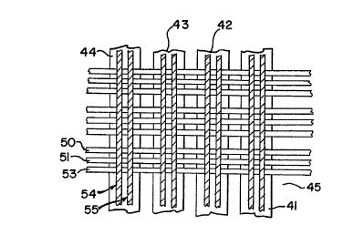
Referring to FIG. 3 there is shown a top plan
view of a partial section of an electrophoretic
display made according to a second implementation.
The top plan view of FIG. 3 show the structure prior
to a final coating of silicon dioxide. Essentially,
as seen from FIG. 3, the cathode lines which are
deposited as described above, are designated by
references numerals 41, 42 and 43. Disposed on top of
the cathode lines and insulate therefrom are separate
grid tine structures as 50, 51 and 53. The three tine ..
structures 50, 51 and 53 represent for example, a
single grid line. Aligned parallel with the cathodes
WO 92/2l733 PGT/US91/03759
-15-
are the second anode lines designated by reference
numerals 54 and 55 as associated with the cathode line
44. As will be explained the grid lines as 50, 51 and
53 are fabricated from a different metal than the
second anode lines 54 and 55 constitute two lines for
each cathode but may be more than two. The grid lines
constitute three lines as 50, 51 and 53. The
implementation of the display as well as the
fabrication of the display can be best described by
referring both to FIG. 3 and FIG. 4. As seen in FIG. ,
4, the bottom layer 45 which consists of glass has
deposited thereon the ITO cathode layers as 41, 42, 43
and 44. The cathode matrix is fabricated as described
above and is formed from a single layer of ITO which
covers the entire glass sheet which ITO is then
suitably etched or engraved to produce individual
parallel cathode lines as 41, 42, 43 and 44. Thus the
construction of the cathode is implemented utilizing
the usual mask and procedures as described above. The
next thing that occurs is that a complete layer 60 of
FSC-L or FSC-M is deposited on and coats the entire
cathode structure. Then a layer of silicon dioxide 61
is vapor deposited on or oxidized on the insulating
layer 60. The next step in the procedure is to then
deposit a layer of metal such as chrome which is layer
62 and deposited on the silicon dioxide layer 61.
This layer of metal 62 constitutes the grid structure.
A layer of photoresist is then spun on the metal layer
62. This layer is not shown. In any event, the layer
of photoresist is then exposed by the grid mask in the
usual manner and hence, one produces the grid line
pattern as for example, 50, 51 and 53 on the
photoresist layer which is spun on the metal layer 62.
The grid mask is used to expose the photoresist in the
WO 92/2Z733 PCT/US91/03759
~, ~r~16- ,...
usual manner. After developing the photoresist, the
metal is etched using a suitable etchant. As
indicated, the metal layer 62 is chrome and one would
then employ a chrome etchant. The photoresist layer
is now stripped off in an appropriate solvent. The
layer of silicon dioxide 61 is now plasma etched with
the etched metal 62 serving as a mask. This therefore
develops the appropriate grid structure. Next an
insulating layer of FSC-L or FSC-M is deposited on the
patterned metal layer and designated by referenced ,
numeral 65. The insulative layer 65 is now coated
with a thin layer of silicon dioxide 4. Deposited on
top of the layer of silicon dioxide 64 is a second
metal layer 63 which may be of a different material
than the first layer. This layer 63 consists of two
metal layers with a first layer of metal closest to
the silicon dioxide layer 64 being the same as the
first layer of metal 62. Each layer is capable of
being etched by a different etchant. A layer of
photoresist is now spun on the uppermost metal layer
and completely covers the same.
It is understood that while the layers 63, 64 and
65 are shown as upstanding columns, it is expressly
understood that these are distinct layers. After a
top layer of photoresist is spun on the uppermost
metal layer, a mask including tines similar to but not
necessarily the same as the grid is placed on a
photoresist such that the pattern is parallel to the
cathode as 41 and 42 and perpendicular to the grid as
grid line 62. After developing the photoresist, both
metal layers are etched using appropriate etchants.
The silicon dioxide layer 64 is plasma etched using ..
the metal layers as composite layer 63 as a mask.
Both the first and second layers of FSC-L or Fsc-M are
WO 92/21733 PGT/US91/03759
-1~- 211 ~ ~ 9 7
plasma etched down to the cathode as seen in the top
view. Using an appropriate solvent, any residue from
the plasma etching is removed. Then a coating of
silicon dioxide is applied to the entire structure.
Again, using an appropriate etchant, the uppermost
layer of metal is removed thereby removing the silicon
dioxide covering the metal and leaving the second
layer of metal exposed. Using appropriate insulator
spacers the remote anode is attached to the structure
making sure that a lead is made available for ,
connecting to the anode. The second layer may be
connected with a11 leads in parallel, with each lead
individually driven or with leads being driven in
groups. The cell is now ready for accepting driver
chips cemented and bonded in the usual manner.