Note: Descriptions are shown in the official language in which they were submitted.
21 10368
WIDE DYNAMIC RANGE NON-UNIFORMTTY
COMPENSATION FOR INFRARED FOCAL PLANE ARRAYS
BACKGROUND OF THE INVENTION
1. Technical Field
The present invention relates generally to infrared
imaging devices and, more particularly, to a method and apparatus for
compensating for the non-uniformity of response of the detector elements of
an infrared focal plane array.
2. Discussion
Infrared imaging devices convert invisible infrared energy
into useful forms such as visible images. This is accomplished by first
detecting infrared radiation which is emitted or reflected from objects in a
field of view and then producing resultant data corresponding to the level
of the infrared radiation that is detected. Generally, infrared imaging
devices include an optical system for receiving the infrared radiation,
detector elements, such as in a focal plane array, for producing a response
corresponding to the level of the infrared radiation received through the
optical system, an electronics unit for processing the response produced by
the detector elements and generating a corresponding digital output, and
may also include an output display unit, such as a cathode-ray tube (CRT),
for displaying a resultant visible image, if desired.
The operation of an infrared imaging device may generally be
described as follows: the optical system surveys a field of view and causes
infrared radiation to be directed toward the detector elements, each of
which correspond to discrete points, or pixels; each detector element then
generates an analog response, such as a voltage or current, corresponding to
the level of the infrared radiation received by that detector element; the
analog response is then processed in the electronics unit which produces a
digital signal output; and, finally, the output is converted into a useable
..~'. k
2110368
form, such as a visible image generated by an output display unit.
Typically, this procedure is continuously repeated for generating a series of
useable data in near real-time, depending upon the imaging application
desired to be performed.
However, through experience it has been learned that because
each individual detector element in a focal plane array is not identical, each
detector element may produce a different response to a given level of
infrared radiation that it receives. That is, a detector element "A" and a
detector element "B" may be exposed to the same level of infrared radiation,
however, each detector element may generate a unique analog response. In
addition, the converse may also be true. That is, a detector element "A" and
a detector element "B" may be exposed to different levels of infrared
radiation, however, each detector element may generate the same analog
response. This phenomenon is well-known as "non-uniformity of response"
or, simply, "non-uniformity." It has also been learned that the relationship
between the response produced by a detector element in relation to various
levels of infrared radiation is non-linear.
Consequently, infrared imaging devices must compensate for
the variations between detector elements and correct them to an "absolute
scale" in order to produce consistent and reliable image data.
A means to accomplish the necessary "non-uniformity
compensation" so that accurate image data may be generated by the infrared
imaging device has been to calibrate each detector element in the focal plane
array with the electronics unit. In this manner, the electronics unit produces
a "corrected" digital signal output which reflects a "normalized" value for
the level of infrared radiation that is received by a given detector element.
Typically, non-uniformity compensation has been accomplished by the use
of a two-point or a four-point calibration method having analog gain and
offset adjustments. However, this technique has presented the disadvantage
of allowing the analog response of any particular detector element to be
compensated for non-uniformity only over a narrow dynamic range of
levels of infrared radiation. Therefore, previous non-uniformity
21 10388
compensation schemes have been inadequate where the field of view of the
imaging device has contained a wide dynamic range of levels of infrared
radiation, such as a "cold" sky and a "hot" terrain.
In light of the forgoing discussion, it is an object of an aspect of
the present invention to provide a method and apparatus for non-
uniformity compensation for use in the focal plane array of an infrared
imaging device capable of compensating for non-uniformity over a wide
dynamic range of levels of infrared radiation. In addition, it is an object of
an aspect of the present invention to provide a focal plane array uniform
response which can be calibrated as an absolute radiometer.
SUMMARY OF THE INVENTION
According to the teachings of the present invention, a method
and apparatus for non-uniformity compensation for infrared focal plane
arrays of an infrared imaging device is described as including a calibration
operation and a correction operation. The calibration operation measures
the responses generated by the detector elements in the focal plane array to
a wide range of known levels of infrared radiation that are produced by a
uniform black body in a controlled environment. The responses are then
stored in a data storage device. The correction operation compensates a
second response of the detector element to the level of infrared radiation
produced by objects in the field of view surveyed by the imaging device by
comparing the second response to the set of first responses and interpolating
the second response to a corrected value.
The present invention is expected to provide non-uniformity
compensation for infrared focal plane array response over a wide dynamic
range of levels of infrared radiation, such as a "cold" sky and "hot" terrain.
In addition, the present invention is expected to be capable of being
performed in near real-time. Further, the non-uniformity compensation of
the present invention can provide focal plane array response which can be
calibrated as an absolute radiometer. Still further, it is believed that the
v::
.,~' :.'~a
21 10368
present invention will enable robust target acquisition and tracking
capability to be achieved in infrared imaging devices, which is necessary for
those infrared imaging devices used in air-to-air missile applications (i.e.
seekers).
Other aspects of this invention are as follows:
A method for non-uniformity compensation for infrared focal
plane arrays comprising the steps of:
(a) measuring each set of first responses generated
by each detector element in said focal plane array
to a wide range of known levels of infrared
radiation produced by a uniform black body in a
controlled environment;
(b) storing said set of first responses in a data
storage device;
(c) measuring a second response of said each
detector element in said focal plane array to the
level of infrared radiation produced by objects in
a field of view;
(d) comparing said second response to said set of
first responses of said each detector element; and
(e) compensating said second response to a
corrected value;
whereby said second response of said each detector element in said infrared
focal plane array is compensated for non-uniformity over a wide dynamic
range of levels of infrared radiation.
A method for non-uniformity compensation for infrared focal
plane arrays comprising a calibration operation and a correction operation,
wherein said calibration operation comprises measuring a set of first
responses generated by each detector element in said focal plane array to a
wide range of known levels of infrared radiation produced by a uniform
black body in a controlled environment and storing said set of first
.._ 2 1 1 p3g8
responses in a data storage device, said calibration operation being
performed for each said detector element in said focal plane array, and
wherein said correction operation comprises measuring a second response
of said each detector element in said focal plane array to the level of
infrared
radiation produced by objects in a field of view, comparing said second
response of each detector element to said set of first responses of each
detector element and compensating said second response to a corrected
value.
In an infrared imaging device of the type having an optical
system, detector elements in a focal plane array, and an electronics unit,
whereby said optical system surveys a field of view causing infrared
radiation to be directed toward said detector elements in said focal plane
array, said detector elements generate a response corresponding to the level
of said infrared radiation, said electronics unit processes said response and
produces an output, said infrared imaging device including non-uniformity
compensation for infrared focal plane arrays comprising calibration means
and correction means, wherein;
said calibration means comprises means for measuring a set of
first responses generated by each said detector element in said focal plane
array to a wide range of known levels of infrared radiation produced by a
uniform black body in a controlled environment and
means for storing each said set of first responses of each said
detector element, and wherein
said correction means comprises means for measuring a
second response of each said detector element in said focal plane array to
the level of infrared radiation produced by objects in a field of view,
means for comparing said second response of each said
detector element to said set of first responses of said detector element and
means for compensating said second response to a corrected
value.
BRIEF DESCRIPTION OF THE DRAWINGS
21 10388
The various features and advantages of the present invention
will become apparent to one skilled in the art upon reading the following
specification, in which:
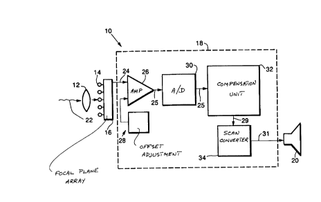
FIG. 1 is a simplified block diagram illustrating an infrared
imaging device incorporating the non-uniformity compensation for infrared
focal plane arrays of the present invention;
FIG. 2 is a simplified block diagram further illustrating the
compensation unit of the infrared imaging device of FIG. 1;
FIG. 3 is a simplified graph showing the non-linear response
curve of an individual detector element in the focal plane array calibrated
over a wide range of levels of infrared radiation which have been linearly
normalized; and
FIG. 4 details a portion of the simplified graph of FIG. 3.
DESCRIPTION OF THE PREFERRED EMBODIMENT
It should be understood from the outset that while the
following discussion illustrates a particular embodiment of the present
invention, this embodiment merely represents a best mode of currently
practicing the invention and other modifications may be made to the
particular embodiment without departing from the spirit and scope of the
invention.
Referring now to FIGS. 1 and 2, an infrared imaging device 10
incorporating the non-uniformity compensation for infrared focal plane
arrays of the present invention is illustrated. As previously described and
as shown in the simplified block diagram of FIG. 1, the infrared imaging
device 10 generally may include an optical system 12, detector elements 14
in a focal plane array 16, an electronics unit 18 and an output display unit
20. As the optical system 12 surveys a field of view, infrared radiation 22 is
received at each detector element 14 in the focal plane array 16. In turn,
each detector element 14 generates an analog response 24, such as a current
P ,..
.,W.,. .;i......
21 10388
or voltage, corresponding to the level of the infrared radiation 22 that it
receives. The analog response 24 is then processed through the electronics
unit 18 to ultimately produce an analog video output signal 31 that is
converted into a visible image by the output display unit 20.
As shown in FIG. 1, the electronics unit 18 includes an
amplifier 26, an offset adjustment 28, an analog-to-digital converter 30, a
compensation unit 32 and a scan converter 34. As further illustrated in FIG.
2, the compensation unit 32 includes a comparator 36, look-up table
memory 38, an interpolator 40, a memory buffer 42 and a CPU 44.
As will be further described herein, the non-uniformity
compensation for infrared focal plane arrays of the present invention may
be best understood as encompassing both a calibration operation and a
correction operation.
CALIBRATION
As already discussed, the analog response 24 of an individual detector
element 14 in the focal plane array 16 to a given level of infrared radiation
22 is not uniform and may vary detector element 14 to detector element 14.
In addition, other factors such as the period of time that the detector
element
14 is exposed to the infrared radiation 22, or integration time, the bias
voltage setting of the detector element 14 in the focal plane array 16 and the
ambient temperature of the environment in which the detector element 14
operates, also affect the analog response 24 generated by the detector
element 14. The purpose of the calibration operation of the present
invention is, therefore, to determine the variations in the analog response 24
of each detector element 14 in the focal plane array 16 over a wide-range of
levels of infrared radiation 22 in a controlled environment, so that these
variations may be recorded for later use in the near real-time correction
operation of the present invention.
Referring once again to FIG. 1, during the calibration
operation, the infrared imaging device 10 is exposed to a uniform black
body (not shown) which uniformly emits a known level of infrared
2 1 10388
8
radiation 22. Each detector element 14 in the focal plane array 16, therefore,
receives the infrared radiation 22 and generates an analog response 24. As
each detector element 14 generates a response 24, the response 24 is
subsequently carried to the electronics unit 18. At the electronics unit 18,
the
analog response 24 is first amplified 26 and offset 28 to match the analog-to-
digital converter 30. In a well-known manner at the analog-to-digital
converter 30, the analog response 24 is converted into a digital video signal
25, which may be a digital word nominally twelve bits wide, for example.
Next, the digital video signal 25 is carried to the compensation
unit, shown as block 32 in FIGs. 1 and 2. As best illustrated in FIG. 2, at
the
compensation unit 32 the incoming digital video signal 25 is directed to the
memory buffer 42, where it is temporarily stored. For the purpose of
enhancing the accuracy of the calibration operation, the focal plane array 16
is exposed to the infrared radiation 22 from the uniform black body (not
shown) over several integration times, or over multiple "frames'. Thus,
multiple digital video signals 25 are generated, each corresponding to an
analog response 24 of the detector element 14 for a separate frame, and are
recorded in the memory buffer 42. These digital video signals 25 are then
averaged by the CPU 44 so as to reduce the negative effect of any
background radiation, or noise, which may influence the value of each
analog response 24 generated by the detector element 14, to a desired level.
It has been found that sixteen separate frames sufficiently reduce such
temporal noise. However, depending upon the amount of background
noise which may adversely affect the analog responses 24 of the detector
element 14, greater or fewer frames may be required. It is important to note
that during an integration time, the bias voltage and ambient temperature of
the focal plane array 14 are held to a known constant value. In this manner,
an "absolute scale" may be generated for the focal plane array 16 against
which the later, individual analog responses 24 of the detector elements 14
may be measured in near real-time during the correction operation.
The resultant average digital video signal 27 is then retrieved
from the memory buffer 42 by the CPU 44 and is stored in the look-up table
2110388
9
memory 38. It should be appreciated that the calibration operation is
repeated, as desired, over a range of infrared radiation levels by varying the
level of the infrared radiation emitted by the uniform black body. It has
been determined that as many as sixteen separate levels of infrared
radiation, or more, may be desired to achieve the wide dynamic range of
non-uniformity compensation of the present invention. Further, it is
important to note that the range of infrared level values over which the focal
plane array is calibrated generally depends upon the specific requirements
that are desired to be met by the infrared imaging device. For example, it
may be desired that the infrared imaging device have the capability to
operate over a wide range of levels of infrared radiation yet maintain a
resolution between two particular levels that is greater than the resolution
over the entire range of levels.
The calibration operation is repeated so that an average digital
video signal 27 for each detector element 14 in the focal plane array 16, at
each of the desired levels of infrared radiation 22, is stored in the look-up
table memory 38. Upon completion of the calibration operation, therefore,
the look-up table memory 38 holds an "absolute data set" of digital video
signals 27 of the detector elements 14 in the focal plane array 16. As shown
in FIG. 2, the look-up table memory 38 has sixteen pages 39, each page 39
containing the average digital video signal 27 for every detector element 14
in the focal plane array 16 at a particular level of infrared radiation 22.
With reference now to FIG. 3, a simplified graph of the response curve
of an individual detector element 14 in the focal plane array 16, after
completion of the calibration operation over a wide range of levels of
infrared radiation 22, is shown. It should be noted that the response v of the
detector element 14 generally increases in relation to the increase in the
level
of infrared radiation ~ to which it is exposed, at a non-linear rate. It
should
be further noted that FIG. 3 shows the levels t to be normalized; that is, the
actual values of the levels of infrared radiation t have been transposed or
"mapped" to different values. Here, the level i has been normalized
linearly. It should be appreciated that the normalization of levels of
:,.
-- 2110368
infrared radiation is well known in the art and may vary depending upon
the desired results to be achieved by the imaging device. Thus, after
normalization, there are sixteen "mapped" levels M. In FIG. 3, because the
normalization is linear, each of the mapped values is separated by a
constant value delta 0.
In addition to the level of infrared radiation 22 to which the detector
elements 14 in the focal plane array 16 are exposed, it should be appreciated
that the other factors, such as the integration time, bias voltage and/or
ambient temperature, may be varied in any combination during the
calibration operation to compile an extremely wide ranged "absolute data
set" for storage in the look-up table memory 38. Again it should be
appreciated that the decision as to which of the above mentioned factors
should vary and which should be constant, as well as their actual values,
will depend upon the operating specifications or parameters required to be
met by the infrared imaging device.
CORRECTION
In use, the non-uniformity compensation of the present
invention is implemented in an infrared imaging device by means of a near
real-time correction operation. As already described, an analog response 24
is generated by each detector element 14 in the focal plane array 16 which
corresponds to the level of infrared radiation 22 that it receives. The
response 24 is carried to the electronics unit 18 and is converted to a
digital
video signal 25, as mentioned earlier. At this point, however, the digital
video signal 25 is carried to the compensation unit 32 and the correction
operation of the present invention is initiated.
Turning once again to FIG. 2, the digital video signal 25 is
shown to be carried simultaneously to the comparator 36 and the
interpolator 40. At the comparator 36, the incoming digital video signal 25
corresponding to the response 24 of a detector element, i, is compared with
the stored average digital video signals v for that detector element 14 in the
r
21 10368
m
pages 39 of data stored in the look-up table memory 38 during the
calibration operation. Upon comparison, the comparator 36 identifies the
stored values v for the detector element i which bound the incoming digital
video signal 25. That is, as shown in FIG. 4, the comparator 36 determines
the stored value v that is greater than, vh, and the stored value that is less
than, ~, the incoming digital video signal 25.
As shown by FIGs. 2 and 4, output from the comparator 36, vh, v~ , and
M~, are carried to the interpolator 40. At the interpolator 40, the digital
video signal 25 is corrected for non-uniformity to a compensated digital
video output signal 29 according to the following equation:
Compensated Output 29 = Ml + [(v~ vl) / (vh-vl) ]0
Although the above equation uses linear interpolation, any
form of mathematical interpolation may be used, depending upon the
accuracy required in the non-uniformity compensation operation.
At this point, the compensated digital video output signal 29 is
carried to a scan converter 30 where it is converted back into an analog
video signal 31 in a well-known manner. From the scan converter 30, the
compensated video output signal 31 leaves the electronics unit 18 and is
carried as input to the output display unit 20. At the output display unit 20,
the compensated video output signal 31 is converted into a visible image in
a well-known manner.
It should be understood that the correction operation of the
present invention is continuously repeated as each detector element in the
focal plane array generates a response to the level of infrared radiation that
it receives.
The present invention is expected to provide non-uniformity
compensation for infrared focal plane array response over a wide dynamic
range of levels of infrared radiation, such as a "cold" sky and "hot" terrain.
In addition, the present invention is expected to be capable of being
performed in near real-time. Further, the non-uniformity compensation of
~ 1 1 0388
12
the present invention can provide focal plane array response which can be
calibrated as an absolute radiometer. Still further, it is believed that the
present invention will enable robust target acquisition and tracking
capability to be achieved, which is necessary for infrared imaging devices
used air-to-air missile applications (i.e. seekers).
Various other advantages and modifications will become
apparent to one skilled in the art after having the benefit of studying the
teachings of the specification, the drawings, and the following claims.
~*