Note: Descriptions are shown in the official language in which they were submitted.
-` 2 ~
IMPROVEMENT TO C:APACITIVE COUPLED POWER SUPPIJIES
BACKGROUND OF THE_INVENTION
~ he disclosed invention is generally directed to
rectifying power supplies, and is more particularly direct-
ed to a high ~requency rectifyinq power supply which doesnot utilize a complex transformer.
Rectifying power supplies are utilized in certain
applications where the required supply voltage is DC. The
originating power source may provide an AC voltage or a DC
voltage. With a DC voltage supply, stepping the voltage up
or down requires conversion of the DC power to AC power
which may be accomplished, for example, with a ~quare wave
converter or a sinewave converter. The AC voltage is then
stepped up or down, as required, by a transformer and then
rectified.
.:
Significant improvements in the size and weight of
rectifying power supplies have been made by increasing the
operating frequency of the AC power. Particularly, higher
operating frequencies allow for significantly smaller
capacitive elements. However, with increased AC operating
frequencies, transformer isolation is reduced, reflections
increase, and core losses increase. As a result of prob-
lems encountered with increased frequencies, di~ferent
transformer designs have been made in attempts to allow ~or
higher AC operating frequency operationO Such designsl
however, are complex and generally require time-consuming
::
~... ,,,,,,,
~"
~,r~
3 ~ 7 ~
and costly development for particular applications.
Moreover, transformers tend to be the cause of the majority
of power supply failures.
A further consideration in the implementation of high
frequency power supplies is the power handling limits of
available diodes. If the number of secondary windings is
reduced in attempting to make transformers smaller and less
complex, then the power limits of available diodes may be
exceeded~ If more secondary windings are used to accommo-
date the power limits of available diodes, then transformercomplexity and size increase.
Another consideration in the implementation of high
I frequency power supplies is the use of inductors which are
¦ lossy and expensive.
SU~DMARY OF THE INVENTION
It would therefore be an advantage to provide a high
frequency rectifying power supply which does not utilize a
complex and bulky transformer.
Another advantage would be to provide a rectifying
power supply that has a reduced number of inductors.
The foregoing and other advantages are provided by the
invention in a power supply which includes an AC current
source operating at a frequency of at least 100 KHz, a
I plurality capacitors responsive to the AC power for provid-
¦ ing DC isolation and for providing capacitively coupled AC
power, and a plurality of AC currenk to DC voltage rectify-
ing circuits that are responsive to the capacitively
coupled AC power for providing respective DC output voltag-
esO
;
~~J C~ Y~ 1
BRIEF DESCRIPTION OF THE DRAWINGS
The advantages and features of the disclosed invention
will readily be appreciated by persons skilled in the art
5from the following detailed description when read in
conjunction with the drawing wherein:
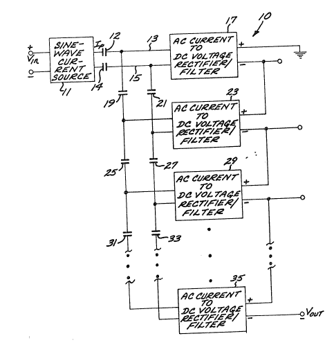
FIG. 1 is a block diagram of a rectifying power supply
in accordance with the invention wherein the outputs of the
power supply AC current to DC voltage rectifier/~ilter
¦ 10modules are serially coupled.
FIG. 2 is a schematic diagram of an AC current to DC
voltage rectifier/filter module that can be utilized in the
power supply of FIG. 1 and in the power supplies of FIGS.
5 and 6.
15FIG. 3 is a schematic diagram of a ~urther AC current
to DC voltage rectifier/filter module that can be utilized
in the power supply of FIG. 1 and in the power supplies of
FIGS. 5 and 6.
FIG. 4 is a schematic diagram of a further AC current
20to DC voltage rectifier/~ilter module that can be utilized
.in the power supply of FIG. 1 and in the power supplies of
FIGS. 5 and 6.
FIG. 5 is a bloc~ diagram of a further rectifying
power supply in accordance with the invention.
25FIG. 6 is a block diagram of another rectifying power
~ supply in accordance with the invention.
''I! 1 DETAILED DE.5CRIPTION OF THE DISCLOSURE
In the following detailed description and in the
several Eigures of the drawing, like elements are identi-
fied with like reference numerals.
Referring now to FIG. 1, illustrated therein is a high
frequency rectifying power supply 10 which includes a
sinewave current source 11 that is responsive to a DC
~ .
1,'
I supply voltage Vin and provides an alternating current
output having a frequency of at least 100 KHz. The sine-
wave current source 11 can comprise known circuitry for
I converting a DC ~oltage to an AC current that varies
1 5 sinusoidally. Alternatively, a square wave current source
may also be utilized.
The curren~ output of the sinewave current source 11
has a peak amplitude denoted Ip and is provided on AC output
lines 13, 15. A pair of coupling capacitors 12, 14 have
their first terminals connected to the output lines 13, 15,
and their second terminals connected to the AC input of an
~ AC current to DC voltage rectifier/filter module 17.
¦ Illustrative examples of circuitry that could be utilizfd
¦ to implement the AC current to DC voltage rectifier/filter
module 17, as well as the other AC current to DC voltage
rectifier/filter modules in the power supplies disclosed
herein, are discussed further herein conjunction with FIGS.
2 ~ 4. The invention employs AC current to DC voltage
rectifier/filter modules for compatibility with the AC
current source in order to reduce diode loss that would
otherwise be greater if an AC voltage to DC voltage recti-
fier modules were utilized. Briefly, an AC current to DC
voltage rectifier/filter module avoids the effect of series
inductors by avoiding the use of inductors or by including
a common mode or coupled inductor which has no DC flux in
its core.
The second terminals of the coupling capacitors 12, 14
; are further connected to the first terminals of further
coupling capacitors 19, 21 which have their second termi-
nals connected to the AC input of an AC current to DC
voltage rectifier/filter module 23, which may be of the
same circuit structure as the AC current to DC voltage
rectifier/filter module 17.
The second terminals of the coupling capacitors 19, 21
3S are further connected to the first terminals of coupling
'~'
.`
^` 2~ ~3 ~
capacitors 25, 27 which have their second terminals con-
nected to the AC input of an AC current to DC voltage
rectifier/filter module 29, which may be of the same
circuit structure as the AC current to DC voltage rectifi-
er/filter modules 17, 23 discussed aboveO
The second terminals of the coupling capacitors 25, ~7
are further coupled to the further coupling capacitors 31,
33 which have their second terminals connected to an
associated AC current to DC voltage rectifier/filter module
~not shown).
~s shown in FIG. 1, N AC current to DC voltage recti-
fier/filter modules may be utilized, the AC current to DC
voltage rectifier/filter modulP 35 being the Nth module,
with all of the AC current to DC voltage rectifier/filter
modules having associated coupling capacitors. In essence,
a pair of coupling capacitors is associated with each of
the AC current to DC voltage rectifier/filter modules and
the pairs of coupling capacitors are serially connected
such that the AC current to DC voltage rectifier modules
are connected at the nodes between pairs of capacitors,
except for the last AC current to DC voltage rec~
tifier/filter module which is connected to the second
terminals of the coupling capacitor pair that is last in
; the series.
As also shown in FIG. 1, the outputs of the AC current
to DC voltage rectifier/filter modules are connected
serially to provide a maximum output voltage that is the
sum of the respective output voltages. As discussed
. further below with respect to FIGS. 2 and 3, the DC voltage
outputs of the AC current to DC voltage rectifier/filter
modules can be across respective output filter capacitors,
and with such structure~ the output capacitors of the AC
current to DC voltage rectifier/filter modules would be
serially connected. As indicatPd in FIG. lt the fixst
terminal of the output capacitor of the AC current to DC
~:~
2 ~ 7 1
voltage rectifier/filter module 17 is coupled to a common
reference potential, which may be considered ground, and
all output voltages are with respect to that common refer-
ence potential. The second terminal of the output capaci-
tor of the AC current to DC voltage rectifier/filter module17 i5 connected to the first terminal of the output capaci
tor of th~ AC current to DC voltage rectifier/filter module
23, and so forth. The second terminal of the Nth AC current
to DC voltage rectifier/filter module 35 provides a high
voltage output which is the sum of the outputs of all of
the AC current to DC voltage rectifier/filter modules. The
outputs respectively provided by the other rectifier/filter
modules should be readily evident.
Assuming small losses in the coupling capacitQrs, the
sinewave current source will need to provide a peak to peak
voltage that is approximately l/N times the DC load voltage
VOUT ~
It should be noted that the increase in the equivalent
series resistance of the coupling capacitors provides a
limit on the number of rectifier/filter modules that can be
utilized in the power supply 10. For example, for an AC
operating frequency greater than 1 MHz and an input voltage
o~ 200 volts, it has been determined that 20-30 rectifi-
er/filter modules appears to be a reasonable upper limit
with the circuit structure of the FIG. 1. A greater number
may result in unacceptable open loop regulation, while in
a closed loop system the variation would have to be ab-
sorbed in the dynamic range of the power supply lOo
Further, high equivalent series resistance results in high
power dissipation, which results in shorter component
lifetimes. An alternate configuration that addresses these
considerations is discussed further herein relative to FIGo
5. ;
Referring now to FIG. 2, illustrated ther~in is a
schematic of an AC current to DC voltage rectifier/filter
,,
,',
7 2 ~ 3 ~ ~
module 20 which may be implemented as each of the rectifi-
er/filter modules in the power supply 10 of FIG. 1, as well
as in the other power supplies disclosed herein. Specifi-
cally, the AC current to DC voltage rectifier/filter module
20 includes a first pair of serially connected diodes 111,
113, wherein the anode of the diode 111 is conne~ted to the
cathode of the diode 113. A second pair of serially
connected diodes 115, 117 is connected in parallel with the
I ~irst serially connected diode pair, wherein the anode of
1 10 the diode 115 is connected to the cathode of the diode 117,
and the cathodes of the diodes 111, 115 are connected
together and the anodes of the diodes 113, 117 are connect-
ed together. A smoothing capacitor 119 is connected
between the commonly connected cathodes of the diodes 111,
115 and the commonly connected anodes of the diodes 113,
117. The node between the serially connected diodes 111,
113 and the node between the serially connected diodes 115,
117 comprise the AC input to the AC current to DC voltage
rectifier/filter module 20, while the DC voltage output of
the AC current to DC voltage rectifier/filter module 20 is
across the smoothing capacitor 119.
, FIG. 3 schematically illustrates a further AC current
to DC voltage rectifier/filter module 30 which may be
implemented as each of the filter modules in the power
supply 10 of FIG. 1, as well as in the other power supplies
disclosed herein. The AC current to DC voltaye rectifi-
er/filter module includes a pair of serially connected
diodes 53, 55, wherein the anode of the diode 53 is con-
nected to the cathode of the diode 55. A smoothing output
;' 30 capacitor 57 is connected between the cathode of the diode
53 and the anode of the diode 55. ~he node between the
diodes and the node at the anode of the diode 55 comprise
the AC input to the AC current to DC voltage rectifi~
er/filter module 30 while the DC voltage output of the
module 30 is across the output capacitor 57.
.11
~1 :
, ---
2~ ~37~
FIG. 4 schematically illustrates another AC current to
¦ DC voltage rectifier/~ilter module 40 which may be imple-
mented as each of the filter modules in the power supply 10
of FIG. 1, as well as in the other power supplies disclosed
herein. The AC current to DC voltage rectifier~filter
module of FIG. 4 includes a first pair of serially connect-
ed diodes 151, 153, wherein the anode of the diode 151 is
connected to the cathode of the diode 153. A second pair
of serially connected diodes 155, 157 is connected in
. 10 parallel with the first serially connected diode pair,
`3 wherein the anode of the diode 155 is connected to the
cathode of the diode 157, and the cathodes of the diodes
. 151, 155 are connected together and the anodes of the
. diodes 153, 157 are connected together. The dotted termi-
nal of the first winding 161a of a common mode inductor 161
'. having first and second coupled windings 161a, 161b wound
, on a common core 161c is connected to the commonly connect
; ed cathodes of the diodes 151, 155; and the dotted terminal
of the second winding 161b of the common mode inductor 161
2Q is connected to the commonly connected anodes of the diodes
: 153, 157. The non-dotted terminal of the first coupled
winding 161a i5 connected to one terminal of a smoothing
capacitor 159, while the non-dotted terminal of the second ~.
coupled winding 161b is connected to the other terminal of
2S thc smoothing capacitor 159. The node between the serially
connected diodes 151, 153 and the node between the serially
,~ connected diodes 155, 157 comprise the AC input to the AC
current to DC voltage rectifier/filter module 40 of FIG. 4,
while the DC voltage output o~ the AC current to DC voltage
rectifier/filter module 40 is across the smoothing capaci-
tor 159.
It should be noted that the common mode inductor 161
comprises coupled windings 161a, 161b wound on a common
~ core, and is connected with a polarity such that no DC flux
; 35 is produced in the core and the rectifier module 40 oper
`^~ '':
`'`:1
.j
-. 2,,l~3~7'll
ates as an AC current to DC voltage rectifier/filter
module. In particular, as indicated by the polarity dots,
any current that flows to the DC output through one winding
of the ccmmon mode inductor returns through the other
winding, whereby there is no DC flux in the core. I~ a
i differential mode inductor having two windings wound on a
single core were substituted for the common mode inductor
161, then the module would have an LC filter characteristic
and would be an AC voltage to DC voltage converter, which
~ lQ as discussed above is subject to higher diode losses. In
j addition, the DC current in a differential mode inductor
would require a larger core since the currents would
produce a DC flux in the core. In the common mode inductor
161 of the module of FIG. 4, there is no DC flux in the
core and thus can be made very small. Substitution of two
separate inductors for the common mode inductor 161 would
present similar problems as the su~stitution of a differen-
tial mode inductor.
The purpose of the common mode inductor 161 is to
isolate the smoothing capacitor 159 from the ripple voltage
present at the AC input to the AC current to DC voltage
rectifier module 40 of FIG. 4, and urther resists any
tendency for any co~mon-mode-currents to flow out of the
module. This is important when several AC current to DC
voltage rectifier/filter modules in accordance with FIG. 4
are series-connected to form a high voltage converter. By
resisting any common-mode currents, each module is guaran-
teed to share the current provided by the source of AC
current to the different modules. In the absence of the
! 30 common mode inductor 161, the lowest voltage module in a
the series connecte~ modules will draw current first in a
, short pulse, then the second lowest voltage will draw a
pulse of current, and so forth. The common mode inductor
161 insures that each moduile draws current for the ientire
~ 35 cycle of the AC input current.
..,~
".
uj~
2 ~10 3 ~1
I Referring now to FIG. 5, schematically depicted
¦ therein is a high voltage rectifying power supply 50 in
accordance with the invention that includes a sinewave
current source 211 which is responsive to a DC input
voltage ~in and provides an alternating current output
having a frequency of at least 100 KHz. The sinewave
I current source 211 can comprise known circuitry for con-
¦ verting a DC voltage to an AC current that varies sinusoi-
il dally. Alternatively, a square wave current ~ource may
I 10 also be utilized.
i The current output of the sinewave current source 211
J has a peak amplitude denoted Ip and is provided on output
lines 213, 215. The first terminals of coupling capacitors
217, 219 are connected to the sinewave current source
; 15 output lines 213, 215. The second terminals of the capaci-
~ tors 217, 219 are connected to the input of an AC current
! to DC voltage rectifier/ilter module 211 that can be
implemented, for example, in the form of one of the AC
current to DC voltage rectifier/filter modules shown in
FIGS. 2-4, discussed above.
¦ The first terminals of coupling capacitors 223, 225
. are respectively connected to the output lines 213, 215 of
the sinewave current source 211. The second terminals of
the coupling capacitors 223, 225 are connected to the AC
input of an AC current to DC voltage rectifier/filter
. module 227 that can be implemented, ~or example, in the
form of one of the AC current to DC voltage
. rectifier/filter modules shown in FIGS. 2-4, discussed
.
.~ above.
Further AC current to DC voltage rectifier/filter
modules and associated coupling capacitors can be connected
. to the output lines 213, 215 as iliustrated by the N~h pair
.~ of coupling capacitors 229, 231 and the associated Nth AC
. current to DC voltage rectifier/filter module 233.
.
~. '
~.~.
2~ ~ 337~
11
J
In the high voltage rectifying power supply 50 of FIG.
5, each of the AC curre~t to DC voltage rectifier/filter
modules is coupled to the output of the sinewave source 211
via respective coupling capacitors which are connected to
~ 5 the output lines 213, 215.
:~ The outputs of the AC current to DC voltage recti~
¦ er/filter modules 221, 227, 233 are connected in series to
~l provide an output load voltage VOUt. Again assuming small
`~ losses in the coupling capacitors, the sinewave current
~l 10 source will need to provide a peak to peak voltage isapproximately equal to 1/N times the DC load voltage VOUT~
¦ Since the coupling capacitors in the power supply 50 are
'~ not serially coupled as to each other, a greater ~umber of
AC current to DC voltage rectifier/filter modules can be
utilized with the power supply 50 of FIG. 5 than with the
power supply 10 of FIG. 1.
Referring now to FIG. 6 shown therein is a rectifying
power supply 60 which may be utilized to provide lower
, voltages with high current. Specifically, power supply 40
is similar to the power supply 50 of FIG. 5, except that
, the outputs of the AC current to DC voltage
; rectifier/filter modules of the power supply 60 are con-
~ nected in parallel, and the sinewave current source will
: need to provide a peak to peak voltage that is approximate-
. 25 ly equal to the DC output load voltage VOUT. The available
., current will be high as a result of the parallel configura-
~ tion of the outputs of the AC current to DC voltage recti-
:,
. fier/filter modules.
;~' ' ' The following are examples of operating parameters and
component values for the power supply 10 of FIG. 1I where
: the Fg i5 the frequency of the output of the sinewave
. current source 11 which has a peak voltage Ip:
vi~ 300 Vol~s
1.6 A
F3: 1 MHZ
!.~ .
::
;,
. ~ :
:
.
I 12 2~ ' ~371
:1
: 1,875 Volts
31_~ç~ 375 Watts
Capacitors 19 21 25 27 31. 33: .022 ~iF
Diodes 111 113 115 117: Type SPD524, Solid States
Devices, La Mirada, California
, Filter CaPacitor 119: .1 ~iF
l Number of AC current to DC voltaae rectifierlfilter
;l modules: 5
While the foregoing power supply structures hav~ been
discussed as stand-alone circuits, it should be readily
~ appreciated that they can comprise modular building blocks
`i which can be connected in series or parallel to achieve the
desired voltage andlor current outputs.
The foregoing has been a disclosure of a rectifying
power supply structure which eliminates the need for an
expensive and complex transformer, operates at frequencies
of at least 100 KHz, reduces the use of inductors, and
achieves reduced diode loss by driving the rectifying
diodes with a current source. Other advantages provided by
the invention include uncomplicated design with predictable
response, adaptability for a modular structure, adaptabili-
ty for use as compact, inexpensive building blocks, which
reduces cost in both development and manufacturing.
Further advantages of the invention include low stored
.j 25 energy in the power supply, and faster open loop response
for regulated power supply applications. Still further
advantages includes reduced size and weight, and increased
efficiency and reliability. Finally, since the limitations
of high voltage transformers do not come into play, the
disclosed invention allows for AC operating frequencies
!,'' substalltially higher than what is presently practical.
Although the foregoing has been a description and
lllustration of specific embodiments of the invention,
various modi~ications and changes thereto can be made by
3S persons skilled in the art without departing from the scope
~','j ',
2 1 3 0 3 7 1
13
and spirit of the invention as defin,Pd by the following
claims.
:
' ~ '
,