Note: Descriptions are shown in the official language in which they were submitted.
WO92/22140 PCT/US92/047~
-) 21~L03~
DIGITAL-TO-~NAL0G ~:
CONVERTER - PREAMPLIFIER APPARATUS
DESCRIPTION -~
,~
echnical Field
The present i~vention relates generally
to the conversion of a digital audio signal into an
analog audio signal with pre-amplification, and in
! particular, to a microprocessor controlled, single-
bit Pulse Den-~ity Modulated (PDM) digital-to analog
converter (DAC) in~orporating digital and analog
preamplifier stages capable of processing digital
audio data formats toward the generation of low-
noise analog audio signals. Currently, most digital
audio playback devices incorporate single chip,
multi-bit digital-to-analog converter technology
and provide no internal pre-amplification of the
~udio signal.
BACKGROUND OF THE INVENTIoN
7 Prior to the advent of digital audio
technology, where "live" audio performances are
recorded digitally for later playback, sound
recording was performed exclusively in the analog
35 domain generating various formats such as LP
W092/22140 PCT/US9~047~
' '~,.
211038~ 2
albums. Such methods utilized a recording process
which resulted in the impression o~ a "physical
copy" of the analog sig~al into a vinyl disk
creating a "groove" which was "tracked" by a
phonograph needle the physical movement of which
would reproduce an electrical "copy" of the groove.
- This method of sound reproduction, however,
suffered from a nu~ber of problems including a low
signal-to-noi~e ratio (SNR) and audible distortion.
Digital technology sought to overcome these
problems by converting the analog audio signal, at
its source, into a digital format. The conversion
of analog audio signals which are by definition
continuous in nature into digital audio signals
which are discreet in nature is performed by a
process known as quantization which involves taking
a "snapshot" of the analog audio signal at various
points in time and transforming the voltage at that
time to its corresponding digital word, u~ilizing
- 20 one of the standard digital audio formats. The
process of taking snapshots is otherwise known as
sampling and the fr~qu~ncy of sampling is referred
to as the sampling rate.
~ urrently, there are a number of standard
formats of encoded digital audio data including:
AES/EBU, EIAJ CP-340, and S/PDIF. Most digital
technolugy currently uses a 16-bit digital word
format which is the result of the encoding process
and which are later used to reproduce or "recover"
the original analog sound. Accurate reproduction of
the original analog signal requires that the
digital sampling to occur at least twice the rate
of the highest frequency to be digitized. If the
sampling rate is in excess of twice the highest
frequency, then it produces greater accuracy in the
WO 92~22140 PCr/US92/04751 ~
1103~5 ::~
- measurement of the analog signal. This approach to
quantization is known as oversampling.
At present, compact audio disks are a common
media for "storingi' digital audio recordings where
the digital audio data is encoded serially on the
disk. A typical compact disc player optically reads
the digital data off the encoded disc; converts
thAt data using a single chip, multi-bit digital-
to-analog converter to an analog audio ~ignal; and
presents this signal to various output plugs and
pins (RCA, headphones, coaxial) for connection to
analog audio components such as preamplifiers or
power amplifiers. Higher-end digital audio
components in addition to providing analog audio
outputs also provide digital audio outputs which
contain the digital audio data prior to conversion
usually on optical and/or electrical output
connectors.
j One shortcoming of some current digital audio
apparatus is the use of higher order filters to
control the signal-to-noise ratio in the outputted
analog signal. The~e higher order filters tend to
cause both amplitude and phase aberrations due to
the need for cascading. While some compact disc
players a~tempt to compensate for these problems
through the use of oversampling, which tends to
ease reguirements on post conversion filters, these
solutions often fall far short of the audio
performance that high end audio users desire.
Another limitation in some current compact
disc/digital audio designs is the use of the
traditional multi-bit digital-to-analog con~erter
devices. The problem with multi-bit digital-to-
analog converters is the difficulty balancing the
multiple outputs to create a linear signal. This
W092/22140 PCT/US92/047~
2110385
design defect can be overcome by precise balancing
of each separate circuit; however, this solution is
difficult, expensive and unworkable due to further
variations in each bit processor caused by
temperature changes within the unit.
A further limitation of single-chip digital
audio equipment is the introduction of noise
¦ through clock jitter and the failure to isolate
audio circuits from noise-producing sources such as
oscillators. While isolation is desirable, it is
impossible to achieve when a single chip component
is used since they often contain in an integrated
format the various devices which one desires to
separate from one another. Jitter reduction
presents a greater problem that can be reduced by
minimizing the path l~ngth between circuits which
produce the clock signals and circuits which use
the clock signals. However, minimizing the path
length may place the oscillator near the audio
circuits, thus reintroducing noise, creating a
catch-22~ situation.
Accordingly, the present invention seeks to
address the foregoing limitations of the prior art
digital audio equipment by providing an improved
¦ 25 digital-analog pre-amp and converter apparatus
! which comprises a microprocessor controlled single
bit Pulse Density Modulated digital-to-analog
converter with hybrid pre-amplification in both
digital and analog domains toward improving the
3~ recovery of analog audio signals from the digital
format with less distortion and lower SNR.
It is an associated object of the present
invention to provide means of up-sampling the
digital audio data by 128 times the incoming rate
through the use of a finite impulse response filter
WO92/22140 PCT/US92/047~
521103~5
and delta-sigca modulation resulting in a noise-
. shaping converter. -~
Another object of the present invention is to
provide for the utilization of an 18-bit digital
audio format, in place of the common 16-bit format
thereby allowing for higher dynamic range;
obviating the need to truncate data; and providing
lower quantization error.
I As rule of thumb in digital audio technology,
¦ lO it is considered that each additional bit in a
digital audio word contributes 6 dB to system
performance, thus the addition of 2 bits from the
traditional 16-bit digital audio word to the 18-bit
word utilized in the present invention provides an
additional 12 dB of dynamic range amounting to over
a 10% increase from the prior art. The increased
word size in the present invention provides for
future digital audio formats which will tend to
have longer word lengths. Currently, the AES/EBU
format provides for the possibility of 24-bit
; digital words.
~ andling a 24-bit word in a 16-bit digital-to-
analog converter would require major truncation of
the input word to a lÇ-bit length, thus losing the
additional accuracy provided by the remaining 8
bits. As for quantization error, the addition of 2
bits to the 16-bit word provides 4 times as many
quantizable voltage levels, thus allowing for more
; exact measurement of the analog voltage when
converted into digital signals.
One solution in the prior art is to deal with
the smaller digital word size which possesses a
lower dynamic range was to utilize a process known
as dithering. Dithering eliminates harmonic
distortion caused by quantization. However, the
WO92/22140 , PCT/US92/047~1
211038S 6
. .
process tends to create a higher SNR. There are 2
widely used methods for producing the dithering
effect, Broadband-Triangular dither and Weighted
dither.
Accordingly, it is an object of the present
invention to be able to process digital audio
signal data produced by sources using the 16-bit
format as well as to be able to accept up to 24-
bit digital audio words.
Another object of the present invention is t
provide for the automatic adjustment for input word
lengths greater than 16-bits and to properly dither
to 18-bits.
Another object of the present invention is to
provide for hybrid digital/analog volume control. -~
In the prior art, a digital output signal could be
attenuated in either of 2 ways, either in the
digital domain before the digital-to-analog
conversion or in the analog domain after the
digital-to-analog conversion. There are advantages
and disadvantages to each of these approaches.
Implementing attenuation in the digital domain is
done by multiplying the digital word by a gain
value which produces extra precision bits in the
digital audio word which is then dithered and
truncated to the word size of the digital-to-analog
converter. This results in a constant noise floor
during attenuation, thus as the audio signal
becomes smaller, it begins to phase into the
constant noise, thus making digital attenuation
less optimal in low volume situations. ~;
Implementing attenuation in the analog domain
is done with the use of mechanical potentiometers
which are often the source of mechanical problems
and mechanical "wiper noise" which may be most
WO92/22140 PCT/US92/04751 ::
2If 038 j
disturbing at higher gain settings. In addition,
analog attenuation often requires the use of dual
volume potentiometers which require balancing; and
the necessity for connections between the
potentiometer and the analog board which may
introduce additional noise into the audio output.
Analog gain control is however potentially free of
constant background noise that is inherent in the
digital implementation.
Accordingly the present invention implements a
hybrid attenuation scheme where by attenuation in
the "lower" part of the gain range is performed
digitally and attenuation in the "upper" part of
the gain range is performed by analog means.
It is yet another object of the present
invention to providD both Broadband-Triangular and
Weighted dithering alyorithms for user selection to
analyze digital audio data of word length greater
than 18 bits and when volume control is below the
~ digital attenuation threshold.
These and other objects of the invention will
become apparent in light of the present
specification and drawings.
.. , , ~ .. . . - . . . , . :
WOg2/221~0 PCT/US92/04751
' : .,
211038~
DI5CLOSURE QF THE INVENTION
The present invention is designed to provide a
very high guality digital-to-analog conversion for
digital audio signals transmitt~d over any one of
three different standard interfaces. The present
digital-to-analog converter is designed to fit into
a high-end audio system and allows owners o* CD
players, Laserdisc players, digital audio tape
decks or direct broadcast satellitP receivers to
improve upon the digital-to-analog convers ion
accuracy otherwise performed internally by said
existing units. The present invention may serve as
¦ a foundation for further digital in/digital out
devices such as sound processors, equalizers,
crossovers and noise reduction units.
The present invention is designed to receive
as an input any one of several digital audio format
interfaces, including the AES/EBU (AudiG
Engineering Societ~/European Broadcast Union)
format aimed at profesæional audio applications,
I th~ EIAJ (Electronic Industries Association of
¦ Japan) CP-340 format and the 5/PDIF ~Sony/Philips
¦ Digital Interface) format, the later two being
1 25 geared toward consumer applications. In addition,
! any one of these three formats may be received by
the present invention as inputs through any one of
three types of hardware interfaces, namely,
balanced transmission via twisted shielded wire
terminated with three pin "XLR" connectors; single
ended transmission via coaxial cable terminated
with an "RCA" connector; and optical transmission
via optical cable terminated with a "TOSLINK"
connector. The "AES/EBU" format is specified only
for the balanced interface and the S/PDIF format is
WO 92~22140 PCr/~lS92/047~1
211038a
specified only for a coaxial interface, while the
CP-340 is specified for all three.
The present invention supports three industry
standard analog audio output formats. A stereo
headphone output connector corapris ing a three
conductor "phone" jack is provided for connection
to stereo headphones. "RCA'I output connectors are
provided for connection of a "line-level" pre-
amplifier or other similar analog signal processing
device, while a power amplifier may be conrlected
either through balanced left and right c:hannel
"XLR" output connectors or "RCA" connectors.
One goal of ~he present apparatus is to
minimize distortion in the processing of the audio
signal. Through the use of low-order, and therefore
more linear pha~e, filtering and the positioning of
corner frequencies of the analog filters far away
f rom the audio band the present apparatus attempts
to minimize distortion, including distortion caused
by amplitude aberrations versus frequency ("non-
flat'l frequency response) and phase aberrations
versus frequency ("non-linear" phase response). The
use of high-speed analog circuitry with high open
loop gain in the present invention minimizes
intermodulation and ~lew-induced distortion.
In addition the use of one-bit pulse density
modulated digital-to-analog converter technology
serves to minimize distortion. While traditional
multi-bit digital-to-analog converter technology
depends on extremely close matching of each bit-
weight with all of the others in order to achieve
good linearity, the one bit digital-to-analog
converter implemented in the present apparatus has
no matching requirements at all and is inherently
linear. Moreover where digital-to-analog converter
WO92/2214~ PCT/US92/047~1 ~
211038~ lO
distortion is most audible, on ~uiet passages, the
multi-bit digital-to-analog converter performs the
poorest and the one-bit digital-to-analog converter
as implemented excels.
Additionally, the present invention seeks to
minimize noise in the audio signal. Noise is caused
by many of the same things which cause distortion.
Noise is minimized in the present invention through
the implementation of low-jitter clocking of the
digital-to-analog converters, and low-noise v41tage
references for the digital-to-analog converters.
Additionally, the design of the present invention
isolates noise sources from the audio circuitry.
separate p~wer transformers and Cupply voltages for
the digital section and analog section assist in
isolating noise from the audio output signals.
The digital audio interface raceiver present
in the digital stage of the invention incorporates
a on-chip PLL which is used to extract the bi-phase
encoded data and the word clock from the selected
digital audio signal input and generates its
I various output clocks, one of which is the sample
I rate (word3 clock. The analog stage of the present
invention incorporates a high performance PLL which
locks on to the extracted word cloc~. This PLL is
the "main" PLL which provides a very low-jitter
clock for all sensitive circuits. It is known that
jitter, small variations in the clock period, in
sampling clocks used in digital-to-analog
conversion processes reduces the potential signal-
to-noise ratio in the presence of signal, commonly
referred to as dynamic range. Accordingly, special
care has been taken to minimize jitter. The sources
of jitter are many as every component in the signal
path is a potential source. Since no particular
WO92/22140 PC~/US92/047~1
2110~85
11
jitter-producing component dominates, jitter can be
assumed to be a broadband "white" noise which
¦frequency modulates the clock in question.
¦The present invention addresses all three of
the basic methods for reducing clock jitter. The
first is to reduce the bandwidth of the error
¦signal from the output of the phase comparator in
the PLL. Thus if the jitter is assumed to be broad-
band in nature, reduced bandwidth will have the
10result of reducing the total jitter energy ~ed to
the oscillator portion of the PLL. In the present
invention, the bandwidth of the loop filter in the
PLL is extremely low, 2.5Hz, and this is followed
by an additional 2 pole low-pass filter with a
15cutoff (-3dB) frequency of 16 Hæ. Thus, the
spectrum of any jitter present at the output of the
PLL is limited to the sub-audio (less than 20Hz)
band. Since the jitter at the input was previously
assumed to be produced by broadband noise frequency
20modulation of the clock, only those components of
the jitter below the loop cutoff frequency will be
~I passed on to the oscillator and, therefore a
! majority of this j itter energy will be filtered
out.
25The second method of minimizing clock litter
is to use an oscillator as "pure" and jitter free
as possible, as the loop filter will not have any
effect on reducing noise sources which cause jitter
wi~hin the oscillator itself. Accordingly, a
specialized form of voltage controlled crystal
oscillator is used. The primary determining factor
of oscillator purity is the "Q" of, or quality
factor of the reactive components which determine
the oscillating resonant frequency. The higher the
Q of these components, the less they deviate from
WO92J22140 PCT~US92/047~1
2110385 12
their resonant frequency. While low jitter and
therefore high Q are needed for high dynamic range,
the apparatus must be usable with a variety of
digital input sources ha~ing different word rates
5 requiring a wide range of frequency. This problem
is addre~sed by implementing three separate voltage
controlled crystal oscillator circuits, one for
each of the three standardized sample word rates.
' Each voltage controlled crystal oscillator is based
¦ 10 on a quartz crystal oscillating element which has a
! very high Q. The crystals are operated in parallel
resonant mode whereby their resonant frequency can
be adjusted over a very limited range (+/- 300 to
400 ppm) ~y means of adju~ting the load capacitance
presented to them. This load capacitance adjustment
is performed by a varactor diode. The limited
control range ic sufficient to allcw phase lock to
any source device which conforms to the applicable
standards based on the three center frequencies the
apparatus supports and yet is sufficiently limited
~' to preclude undesirable deviation.
j The third method of minimizing clock
¦ jitter is to physically locate the PLL close to the
¦ actual cGnversion circuits thereby minimizing the
! 25 number of potential jitter producing stages between
the PLL output clock and the digital-to-analog
converters.
The main PLL is a frequency multiplying type
taking the sample rate clock (word clock) at 32,
44.1 or 48 KHz and generating a phase synchronized
clock at 256 times this incoming frequency. The
source for the main PLL is the word clock extracted
by the digital audio interface receiver. This
signal feeds the reference input of the phase
comparator. These outputs then enter a differential
WO92/22140 211 0 3 8 ~ PCT/US92/04751
!
13
loop filter built around a precision low-bias
current opamp. Low-bias current is important in
j reducing the sidebands generated in a frequency
multiplying type PLL. The chosen loop filter ha~ a
very low bandwidth and an over damped response to
stay within the limited control range of the
voltage controlled crystal oscillators. The low
bandwidth of the filter and overdamped response
results in a lock time that is long, on the order
of one second.
The loop filter is followed by a 2nd order
lowpass filter having a overdamped response that
does not add any overshcot during acquisition. The
filter output then drives varactor diodes of the
three vol~.age controlled crystal oscillators. The
voltage controlled crystal oscilla ors outputs feed
a digital multiplexer which selects the proper
output and sends this to the divider circuitry. The
divide by 256 circuit is composed of two 4-bit
! 20 synchronous counters, the desired outputs of which
are re-clocked to maintain edge alignment between
all of the outputs. The sample rate output is
returned to the variable input of the phase
comparator thereby closing the loop. Digital audio
data supplied by the external audio sources is
firs~ passed through a digital audio interface
r~cei~er which identifies the sampling rate and
word length associated with the incoming digital
audio data.
Digital audio signal processing is handled by
a 24-bit fixed point digital signal processor
(DSP), and by a 18-bit (input word size) delta-
sigma processor. The DSP is a general purpose
device for which software routines carry out the
desired functions. The delta-sigma processor is a
W~92/22140 PCT/US92/~47
14
21103~5
dedicated processor and is not software dependent.
The DSP performs dithering for input signals
of greater word length than the up-sampling DSM
chip is capable of handling, digital attenuation,
balance, and muting functions.
The delta-sigma processor performs the
function of up-sampling the stereo audio data by
12 8 times the incoming rate by way of a technique
called "delta~sigma conversionl'. This type of
lo conversion is often referred to as a "noise-
shaping" converter. The input is fed to the devicein serial form with up to 18 bits of precision. The
stereo data feeds an 8 times oversampling
¦ interpolation filter which generates 7 intermediate
sample values between each o. the incoming samples
by using a large impulse response filter, resulting
in digital audio data at eight times the original
sampling rate. This data is then fed to the delta-
sigma modulator which operates at 16 times the
input data rate for a total oversampling ratio of
128. The delta-sigma modulator uses a 5th order
, noise shaper which allows the reduction of the word
¦ size down to a single bit per channel at 128 times
the original word rate by shaping the resultant
quantization noise spectrum such that the audio
band has a minimum amount of in-band noise, at the
expense of a large amount of out-of-band noise.
The resulting DSM data is a digital audio data
signal which is clocked at 128 times the incoming
sampling rate determined by the digital audio
inte~face receiver. The data, along with the
associated clock generated by the DSM are
optocoupled onto the analog board.
optocoupling is used to isolate the analog
function on the analog board from the digital IC
WO92/22140 PCT/US92/04751
! 21~ a3 8
chips located on the digital board which generate a
large amount of digital noise~ Optocouplers
effectively transmit the necessary signals between
the digital and analog circuits without requiring
the relatively noisy ~igital board supplies to be
directly connected to the analog circuitry.
Once the serîal digital audio data reaches the
analog board it is reclocked by the main PLL on the
analog board. For example as the delta-sigma
modulator has upsampled the digital audio word by
128, a clock at 128 times the sampling rate
determined by the digit-audio interface receiver is
used to clock a serial-to-parallel shift register
which takes the incoming serial digital audio word
and shifts it one bit at a time. The output of the
Chift register is fed into AND gates with both
regular and inverted inputs. The other input of
each AND gate is either the clock signal or its
; complement. The result of the AND'ing function is
that the digital audio data is present for only
half of a bit cell period. This is called a
"return-to-zero" function. The AND gate outputs are
then reclocked in a D type flip-flop with
complementary outputs, producing both negative and
positive values of the digital word, and then
connected to the one bit digital-to-analog
converter.
The digital-to-analog converter for each
channel is essentially 4 ssts of single pole-double
throw switches the results of which are then fed
into a positive summer and a negative summer. The
output of the summers are fed into a differential
amplifier which changes the sign of the negative
thus subtracting the negative value from the
positive value. This has the effect of filtering
WO92/22140 PCT/US92/047~1
2 11 0~ 85 16
noise which may have occurred in the digital-to-
analog converter and provides the correct analog
audio output. The input to the digital-to-analog
converter is a voltage raference determined by the
gain register.
Implementation of analog gain control is done
through the use of ~2-bit multiplying digital-to-
analog converters, one for each channel. The
multiplying digital-tooanalog converter simply
multiplies the voltage at the reference input b~
the digital value loaded into it. The refe!rence
input to the digital to-analog converter is
supplied by a very low noise 10 volt reference
circuit. The use o~ the 12 bit multiplying digital-
to-analog converter results in a 0.02 dB minimum
~tep ~ize over a 20 dB range or a 0.06 dB step over
a 30 dB range. Log conversions f or the data are
performed by the microcontroller and are fed to the
control register and to the gain register. The
multiplying digital-to-analog converter is a
current output device such that precision opamps
are used to convert the output to a voltage and
thu supplies the reference voltage used by the one
bit PDM digital-to-analog converter.
The output of the digital-to-analog
converter, an analog audio ~ignal, is passed to a
low-pass filter which removes any out-of-band noise
created in the signal processing, and especially in
the dithering and upsampling by the delta-sigma
modulator. The analog audio signal is de-emphasized
if the digital audio interface receiver has found
that the incoming digital audio signal was
preemphasized, having signaled the microprocessor
accordingly. The output of the low pass filter is
passed to an analog output board which contains the
WO 92/22140 PCI~/US92/04751
211 038~
17
power buffers the output of which is a standard
, analog audio output signal which may be used by any
number of standard audio components.
. :~
W~ 92~22140 PCr/US92~047~1.
2110385 18
BRIEF DESCRIPTION OF THE DRAWINGS
Fig. l of the drawings is a simplified block
diagram c)f the functional stages of the present
improved digital-to-analog converter-preamplifier
apparatus;
Fig. 2 of the drawings is a block diagram
illustrating the interconnection of the various
circuit boards which together comprise the present
invention;
FigsO 3A, 3B of the drawings together are a
front elevational view of the front panel of the
present invention illustrating the various con~rols
and LED indicator~;
Fig. 4 of the drawings is a front elevational
view of the back panel of the present invention
illustrating the various input and output
connectors;
Figs. 5A, 5B of the drawings together are a
schematic block diagram of the digital board of the
present invention;
Figs. 6A, 6B of the drawings together are a
detailed functional block diagram of the analog
board of the present invention;
Fig. 7 of the drawings is a functional block
diagram illustrating the generation of clock
signals within the present invention;
Figs. 8A, 8B of the drawings together are a
schematic block diagram illustrating the
microprocessor unit of the present invention;
Figs. 9A - 9C of the drawings together are a
detailed block diagram illustrating the processing
of the audio signal in the digital board of the
invention;
Fig. 10 of the drawings is a schematic circuit
`
WO92/22140 PCT/US92/04751
lg 211 3~85
diagram of the LED drivers for the front panel
indicators;
Figs. llA, llB of the drawings together are a
schematic circuit diagram for the drivers for the
power indicator located on the front panel of the
invention;
Fig. 12 of the drawings is a schematic circuit
diagram of the motor driver circuits for the volume
potentiometer located on the front panel of the
invention; ~:~
Figs. 13A, 13B of the drawings together are a
schematic circuit diagram of the display board for
providing bar indicators on the front panel of
the invention;
Fig. 14 of the drawings is a schematic circuit
diagram of the encoder board for the balance
control knob;
Fig. 15 of the drawings is a schematic circuit
diagram of the power board illustrating th~ power
switch and LED indicator;
Fig. 16 of the drawings is a schematic circuit
diagram of the input selection ~witch array and the
accompanying LED indicators;
Fig. 17 of the drawings is a schematic circuit
diagram of the mute board illustrating the mute
switch and LED indicator;
Fig. 18 of the drawings is a schematic circuit
diagram of the motor board for the volume
potentiometer;
Fig. 19 of the drawings is a schematic circuit
diagram illustrating auxiliary digital signal input
connections on the front panel and associated
selection switch and LED indicators;
Fig. 20 of the drawings is a schematic circuit
diagram of digital signal input connectors located
W092/22140 ` PCT/US9~/047 1
211038S 20 ~
on the rear panel of the present invention;
Fig. 21 of ~he drawings is a schematic circuit
diagram illustra~ing the automation ports located
on the rear panel of the present invention;
1 5 Figs. 2-ZA - 22C of the drawings together are a
¦ schematic circuit diagram illustrating the CPU, ROM
! and RAM components of the digital board;
Fig. 23 of the drawings is a schematic circuit
diagram illustrating the battery backup, the
auxiliary 5 V supply source and the address buffer
for the digital board;
Figs. 24A - 24D of the drawings together are a
schematic circuit diagram illustrating the digital
signal processing integrated circuit and associated
memory and framing GAL on the digital board;
Figs. 25A, 25B of the drawings together are a
schematic circuit diagram illustrating the audio
signal selection multiplexer/digital interface, the
digital audio interface receiver and the interface-
CP~ status register of the digital board; `;
~igs. 26A, 26B of the drawings together are a
schematic circuit diagram illustrating the delta-
sigma modulator, decoding GAL and reset circuitry :
of the digital board;
Fig. 27 of the drawings is a schematic circuit
diagram of the analog latch of the digital board;
Fig~ 28 of the drawings is a schematic circuit
diagram of the power supply monitoring circuit of
the digital board;
Figs. 29A - 29C of the drawings together are a
schematic circuit diagram illustrating the
optocouplers located on the analog board which
provide an interface between the digital board and
the analog board;
Figs. 3OA - 30C of the drawings together are a
~ W092/22140 PCT/US92/04751
2 1 1 0 ~ 8 3
21
schematic circuit diagram of the return-to-zero and
of the analog board;
Fig. 31 of the drawings is a schematic circuit
, diagram of a "divide by 256" circuit; ::
Figs. 32A, 32B of the drawings together are a
schematic circuit diagram of the main phase lock
¦ loop located on the analog board;
I Figs. 33A, 33B of the drawings together are a
¦ schematic circuit diagram of the digital-to-analog
I lO converter voltage reference circuits;
Fig. 34 of the drawings is a schematic circuit
diagram of the left channel digital-to-analog
converter (identical to the right channel digital-
to analog converter);
Fig. 3S of the drawings is a schematic circuit
diagram illustrating the left channel low-pass -~
filter of the analog board (identical to the right
channel low-pass filter);
Fig. 36 of the drawings is a schematic circuit
diagram of the left channel headphone amplifier
(identical to the right channel amplifier); :
Fig. 37, 38 and 39 of the drawings are :
schematic circuit diagrams of the analog board `~
power supply and monitor circuits;
Figs. 40A ~ 40C of the drawings together are a
: schematic circuit diagram of the output amplifier
board of the present invention; and `:
Figs. 41 - 46 of the drawings are flow
diagrams of the software routines downloaded to the
digital signal processor for performing gain
control and dithering of digital audio signal
words. ~:
WO92/22140PCr/US92/04751
. ,i
` ` ; 22
~1103~
BEST~ MODE FQR CARRYlNG ~PT THE INVENTION
~ 5While this invention is susceptible of
¦ embodiment in many different forms, one specific
¦ embodiment is shown in the drawings and will herein
be described in detail with the understanding that
the present di closure is to be considered as an
exemplification of the principles of the p:resent
invention and is not intended to limit the
invention to the embodiment illustrated.
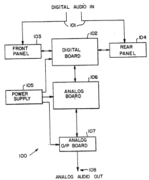
Fig. 1 of the drawings is a simplified block
diagram of the functional stages of the present
improved digital-to-analog converter - preamplifier
apparatus 100. Apparatus 100 accepts as an input
digital audio signa~ data in any one of the
- following digital audio formats: the AES/EBU (Audio
Engineering Society/European Broadcast Union); the
EIAJ (Electronic Industries Association of Japan)
f CP-340; and the S/PDIF (Sony/Philips ~igital
Interface) format. As illustrated, the present
invention is implemented in six major "stages" or
electronic circuit boards, including digital board
¦ 25 102, analo~ board 106, power supply 10S, rear panel
104, front panel 103 and analog output board 1~7.
Power supply 105 as illustrated generates two
regulated voltages of +5V for use on digital board
102 and unregulated voltages for use on analog
board 106.
Front panel 103 incorporates input selection
switches, status LED's and an alpha-numeric
display, which permit the user to select which
digital audio signal provided by the several
connected digital input sources shall be processed
WO92/22140 PCT/US92/~4751
. .
23 211~38S
by the present invention and displays status
information to the u~er. Rear panel 104 contains
the primary input connectors through which the
digital audio signals enter apparatus loQ. Front
panel 103 additionally contains several "auxiliary"
input connectors through which sources of digital
audio signals may ba connected, as may be desired
on a temporary basis, all without having to move
the apparatus to expose the rear panel and possibly
disturb any existing electrical connections.
Digital audio signals 101 are digitally
processed by digital board 102 and are converted
into analog audio signals ~08 by analog board 106.
Digital board 102 serves to provide ~verall control
of apparatus 100 via an on-board microprocessor
which monitors the status of user accessible
- switches and indicates the apparatus status through
front panel LED's and a vacuum fluoresce~t display.
Digital board 102 further processes the supplied
digital audio data by use of a digital signal
proce~sor performing gain control and dithering as
well as generating gain and control information for
use by analog board 106. The output signals of
digital board 102 are left and right channel
digital audio signals presented in serial form at
128 times the original sampling rate of digital
audio input signal 101. The digital audio signals
are passsd to analog board 106 via a series of
optocouplers which protect analog board 106 from
any noise generated by the many components located
on digital board 102. Analog board 106 performs a
number of analog gain op~rations as well as the
digital-to-analog conversion of the digital audio
data, thus generating analog audio outputs which
are sent to analog output board 107 for audio
WO92/22140 PCT/US92~04751
2 1 1 ''~ 3 X ~ 4
buffering and amplification resulting in analog
audio output 108. Also contained in analog output
board 107 are a series of muting circuits which
serve to protect apparatus lOo and the external
audio equipment connected thereto in the event of a
malfunction of apparatus loo. Analog audio output
signal 108 is a stereo audio signal suitable for
connection to conventional audio components for
further pre-amplification, power amplification
and/or further processing, all toward playback of
the audio signal.
Fig. 2 of the drawings is a block diagram
illustrating the interconnection of various m~jor
circuit boards and their subboards which together
lS comprise apparatus 100. Front panel 103 is shown
comprisîng multiple circuit hoards which in
cooperation with digital board 102 serve as the
user interface of apparatus 100 through which the
user controls the operation of apparatus lO0 and
monitors its status. Maîn front panel board llO is
the interface be~ween digital board 102 and the
other circuit boards which together form front
panel 103. Main front panel board 110 also contains
LED latches and drivers as well as motor drivers
along with interface connectors for the other front
panel boards lO9, lll ~ 117.
Front panel power board lll contains the main
power switch and associated LED which the user
depresses to activate apparatus 100. The main power
switch is a soft switch and includes a bicolor LED
status indicator which indicates the three power
conditions of apparatus 100, acti~e, standby and
diagnostics. Front panel power board lll is
connected to front panel switch and LED board 112
which contains switches and accompanying LED' 5
' W092/22140 PCT/US92/047~1 `
2~ 3 8 ~
~hich are operat-d by the u~er in order to select
, which of the digital audio signal connectors will
be enabled toward inputting digital audio signals
to apparatus loo. Both the input select switches
and power switch are then conveyed from front panel
' swîtch and LED board 112 to main front panel board
¦ 110 and then on to the microprocessor which is
contained within digital board 102~ :
¦ ~ront panel status LED and remote receiver
board 113 contains various indicator bars for the
six status conditions, three sampling rate
indicators for 32 KHzl ~4.1 KHz and 48 XHz, and one
! indicator each for l'emphasis", "invert'l and
"validity error". Front panel status LED and remote
receiver board 113 also accepts signals from a
handheld remote control device used by the operator
for adjusting the volume and for operating the
various other controls of apparatus 100. Front
panel status LED and remote board 113 is likewise
electrically connected to main front panel board
110.
¦ Behind door board 114 is a circuit board which
contains various auxiliary inputs and control
switches concealed behind-a door on the front panel
of apparatus 100. Behind door board 114 includes
two auxiliary inputs through which digital audio
signal sources may be connected to apparatus 100. A
headphone jack is additionally provided through
which the analog audio output signal may be
connected to a set of headphones. Behind door board
114 is electrically connected to the microprocessor
on digital board 102 through main front panel boaxd
1~0. Front panel encoder board 115 contains the 32
PPR optical encoder which is driven by the balance
knob on the front panel of apparatus 100. Front
WO 92/22140 PCI/US92/047~1
211038S ` -` 26
panel encoder board 115 is electric:ally connected
to main front panel board 110. ~ :~
Motorized potentiometer board 116 contains the
motor driven volume potentiometer positioned on the
face of the front panel of apparatus 100 . The
motorized potentiometex op~rates on +5V and is
dri~ren by the motor drivers resident on main front :~
panel board 110. Front panel mute board 117
contains the mute switch which when actuated mutes
the output volume of apparatus 100 with the status
of said mute switch being displayed by an
accompanying LED. ~:
Vacuum fluorescent display board 109 is
electrically connected to main front panel board
110 and contains an alpha-numeric vacuum
fluorescent display through which status messages
and warnings are communicated by apparatus 100 to
the user.
The digital audio signal data 101 connected to
rear panel board 104 and front panel 103 by way of
behind door board 114 passes to digital board 102
wher~ it is processed in the digital domain,
including hybrid digital gain control, the output
of which is the digital audio signal in single bit
serial form which is in turn connected to analog
board 106. Analog board 106 is responsible for the
digital-to-analog conversion and the hybrid analog
gain control of the analog output signal. Analog
board 106 sends output to analog output board 107
which buffers the signal prior to attachment to
analog audio components. Analog output board 107
also contains the muting function controlled by the
microprocessor on digital board ~02 as dictated by
power supply monitor circuit on digital board 102
or power supply monitor circuit on analog board
, . . .
WO92/22140 PCT/US92/~4751
~ 211 1)38~. ~
27
. .
;~
o~
Power supply 105 is responsible for accepting
power from a wall outlet and transforming same for
both digital and analog boards utilizing
transformers and regulators to maintaîn the
required voltage re~uirements of +/ 12V, +/-18V,
~SV a~d +~OV~
Figs. 3A, 3B of the drawings together are a
front elevational view of the front panel 120 of
the present invention. Power switch 121 is provided
for the user to select between a "on" mode or a
"standby" mode. Bi-color LED 122 is shown e~bedded
into power switch 121 and serves to indicate to the
user which one of the three possible power states
apparatus 100 is operating in (normal, standby or
diagnostics mode). Input selection switches 123,
125, 127, 129, 131 and 133 are soft switches whose
status is monitored by the microprocessor resident
. on digital board 102. The input selection switches
co~-respond to the various digital signal input
connectors associated with the apparatus and permit
the user to select which external source of digital
audio signals is to be "connected" for on-line
processing. Input ~election switches 123, 125, 127,
i2 9, 131 and 133 are each shown incorporating
embedded LED'S 124, 126, 1~8, 130, 132 and 134
respectively, the illumination of which indicates
that the particular input selection switch is
active.
The user may determine the current status of
apparatus 100 by observing vacuum fluorescent
display (VFD) 135 and the various LED's and bar LED
status indicators provided. In the disclosed
em~odiment of the invention, VFD 135 is a 20-
35 character one line display used to communicate
WO 92~2140 ~ Pcr/~lsg2/047~1 ~
2 1 1 0 3 8 S 2 8 . !
product revision, error messages and other varioususer interfac~ information to the user. Sample rate
; indicators 136, 137 and 138 are each foùr LED-bar-
indicators (providing uniform light intensity)
which indicate to the user the sampl ing rate of the
incoming audio data signal. Infrared remote
detector 13g detects user-inputted commands
generated by a handheld remote control device which
may be used by the user in place of the controls
located on front panel 120 to operate apparatus lOO
(except for output level button 15~ which snust be
manually depressed) . Use of a remc: te control is
reflected in the operation and design of the
associated LED's and motorized volume control knob
146. Emphasis indicator 140 is a LED indicator the
. illumination of which indicates to the user that
i the incoming digital audio data signal selected was
! pre-emphasized by an external audio component.
Error indicator 141 is a LED indicator the
illumination of which indicates to the user that
the incoming audio digital data signal may be
¦ corrupted or invalid. Invert indicator 142 is a LED
¦ indicator the illumination of which indicates that
phase invert switch 156 is in an 'on' position.
- 25 Balance knob 143 is a rotatable knob which
~rives an internal optical encoder generating 32
pulses per revolution (PPR). This signal is
transmitted via front panel encoder board 115 to
main front panel board 110 for connection to the
microprocessor on digital board 102 which reacts
accordingly to alter the left/right channel balance
of the outputted analog audio signal.
Volume control knob 146 is a motorized
potentiometer Which controls the loudness of the
analog output audio signal. Tne analog output audio
WO92/22140 PCT/VS92/04751 ~
2110385
29
signal does not pass through ~he potentiometer
itself, as is done by other conventional devices.
~ather, volume control knob 146 drives a
digital/analog hybrid volume control circuit which,
in turn, controls the loudness of the analog
output audio signal. ~olume LED 147 is a LED
indicator the illumination of which indicates to
user that output level switch 157 is in a variable
position, as opposed to the fixed position, such
that volume control knob 146 is enabled.
- Controls and connectors 149 - 157 are shown
located behind a movable door which when closed
conceals said lesser used controls and connectors,
said controls and connectors being deemed auxiliary
and needing only infre~uent access. Headphone jack
149 is a buffered and amplified headphone jack and
serves to provide a connection point for a
headphone set. Auxiliar~ coaxial input 150 is one
of the possible input locations for digital audio
data. Auxiliary optic 1 input 151 is a "TOSLINK"
input for optical digital audio data as generated
by any of the above mentioned digital audio
components. "Auxiliary 6" button 153 and "auxiliary
7" button 154 are additional input selector
controls to select between auxiliary coaxial input
150 and auxiliary optical input 151, respectively.
Phas~ invert selector 156 is a user selected option
which inverts the phase of the outgoing analog
audio data. Output level selector 157 controls
whether the present invention 100 operates in
variable or fixed gain mode. Digital audio input
signals 158 and 159 connect input connectors 150
and 151 to digital signal input multiplexer 209,
shown in Figs. 5A, 5B.
Fig. 4 of the drawings is a front elevational
WO92/22140 ` PCT~US92/04751
~llQ3~ j 30
view of the back panel 160 of the present invention
100. Outputs 161 and 162 are the left and right
outputs, respectively, containing the processed
analog audio data. Outputs 163 and 164 comprise the
left and right outputs, respectively, in XLR-M
connector format. Output gain selector 173 controls
the fixed gain mode of the output of apparatus 100,
by permitting the user to select between a 0 and
+10 dB attenuation of the output si~nal. Coaxial
input l 165 and coaxial input 2 166 accept digital
audio data from digital audio components on aoaxial
cables and feed the data to lin~s 180 and 1~1,
respectively, which are connected to the digital
j interface (shown on Figs. 5A, 5B~. Optical input-1
167 and optical input-2 168 are "TOSLINK"
connectors which accept digital audio data in
optical form from digital audio equipment and feed
into the digital interface on lines 182 and 183,
respectively. AES/EBU input 169 is an XLR-F
connector which receives digital audio data from
digital audio equipment and places it on line 184
¦ which is then fed into digital interface 207 (as
~ shown on Figs. SA, 5B). Digital automation input
; 170 accepts data input from an RS-232 connector
which is then decoded by an RS-232 decoder (as
shown in Figs. 22A - 22C). Digital automation port
output 171 accepts an RS-485 connector which
transmits data as output from present invention 100
for analysis in debugging and audio translation~
3~ IBC connector 172 provides power to apparatus 100
from a common wall receptacle. Said power is fed
into both the digital power transformer 229 and
analog power transformer 300 by lines 187 and 188
~as sh~wn in Figs. 5A, 5B and Figs. 6A, 6B,
respectively)-
WO~2/22140 PcT/us~2~o475l ~
. 31 21103~ :
~ .
Figs. 5A, 5B of the drawings together are a
schematic block diagram of the digital board 102 of
the present invention 100. LED register 200 is
shown and comprises a series of latches which
contain a copy of the current LED status word as
transmitted through data bus 201 from
microcontroller 215. The output of LED register 200
is used to determine whether LED's 124, 126, 128,
130, 132, 134, 145, 147, 153 and 155 which are
; 1~ located on front panel 120 are illuminated or not.
Switch matrix bus 202 connects microcontroller 215
to the input select æwitches 123, 125, 127, 129,
131, 133, 144, 152, 154, 156 and 157 such that
microcontroller 21S may monitor their respective
~5 positions toward respondiny to user commands. Infra
red detector line 203 connects microcontroller 215
! to the IR remote control detector 139 positioned on
' front panel 20. Volume control motor driver 204
¦ controls volume knob 146 through control signal
~ine 205 in response to the signals generated by
microcontroller 215 communicated through bus 212.RS-232/RS-485 receiver 206 receives data from RS-
232 input 170 as conveyed by line 184 and decodes
said data for input into microcontroller 215.
Receiver 206 also sends output data through line
~8~ to output port 171 which is for use with RS-485
connectors.
Digital interface 207 is the port through
which all of the incoming digital audio data
signals from both front panel 120 and rear panel
160 are received. The outputs of the digital
interface 208 are fed into 7-to-1 multiplexer 209
which is used to select which digital audio data
signals 158, 159, 180 - 183 are to be processed by
apparatus 100. Multiplexer 209 is controlled by
WO92/22140 PCT/US92/~4751
`
211038~ 32
microcontroller 215 which re~p~nds to the position
of input select switches 123, 125, 127, 129, 131,
133, 152 and 154 such that the appropriate
selection code is transmitted by micro~ontroller
215 to multiplexer 209 via multiplexer selection
bus 210. The output of multiplexer 209 is a digital
audio signal which is shown connected to di~ital
audio interface receiver 214 which is a standard
AES/EBU interface device. Digital audio interface
receiver 214 communicates with microcontroller 215
via address bus 21B toward the exchange of data and
various instruction ~odes. Digital audio interface
receiver 214 ~erves to determine the rate at which
the ~elected digital audio si~nal 213 was
originally ~a~pled ( ampling rate~. The sampling
rate ref~rr~d tc herein sometimes as the word clock
"WC/" is transmitted to analog board 106 via line
2340 Digital audio interface receiver 214 is
clocked by clock signal 235 designated as the
"256CLK". The output 232 of digital audio interface
receiver 214 is shown connected to digital signal
processor ~DSP) 224~
In the disclosed embodiment of the invention,
DSP 224 is a commercially available type 56001
digital signal processor integrated circuit which
is suitable ~or digital audio words having a word
length of up to 24 bits in length. DSP 224 is used
to perform gain control and, where necessary,
dithering. DSP output 233 is fed into delta-sigma
modulator 22S which, in the disclosed embodiment of
the invention comprises a digital-to-analog
converter device which is being used solely to
perform the delta-sigma modulation operation.
Delta-sigma modulator output 236 which consists of
left data, right data and the data clock is
,.. . . ..
~ W092/22140 PCT/US92/047~1 ~ - l 332110383
connected to analog board 10~ shown in Figs. ~A,
. 6B.
When apparatus 100 is initially powered up,
the internal programs for DSP 224 are downloaded to
DSP ~24 from EPROM 222 under the cs~ntrol of
~. microcontroller 215 on data and address busses 201
and 218. Downloading of the DSP program directly
onto DSP 224 reduces sys~em costs and allows for
greater processing speed. DSP 224 utilizes SRAM
220, EPROM 222 and address decoder 223 to perform
digital gain, and dithering functions. All data and
addresses used in allowing microcontroller 215 to
control the DSP functions travel through buses 201
and 218 respectively. In addition to controlling
¦ 15 the digital audio data path, microcontroller 215 is
responsible for the control of analog board 106,
front panel 103, rear panel 104 and the remainder
of digital board 102. The microcontroller 215 aIso
utilizes SRAM 220, EPROM 222 and address decoder
223 to carry out its functions and in accessing its
software control instructions. Line 235 is shown
connecting the "256CLK" signal to both digital
audio interf~ce receiver 214 and delta-sigma
modulator 225.
Power to operate digital board 102 is supplied
by power transformer 229 which is connected to an
external source of AC power via lines 187 and 188
which in turn are connected to the IEC connector
172 located on rear panel 160. Digital power supply
228 regulates the power supplied by power
transformer 229 and supplies the various voltages
needed to operate the integrated circuit components
utilized in digital board 102. Digital supply
monitor 227 determines whether the voltage needs of
the digital board 102 can be properly met, detects
WO g2/22140 . . PCr~US92/~47~1
211~3~S 34
any po~er related problems and signals
microcontroller 215 of any such problems should
they occur via c:ontrol line 231 labeled DPFAIL,
(digital board power fail). In addition APFAIL
5 (analog board power fail) line 238 is shown
terminating at microcontroller 215 and likewise
serves to signal a power fail condition in the
analog puwer supply cir::uits.
Figs. 6A, 6B of the drawings together are a
10 schematic functional block diagram of analog board
106 of present invention. Analog board 106
exchanges ~rarious signals with the digital board
102 (as shown on Figs. 5A, 5B) including WC/ 234;
256CLK 235; left data, right data and data clock
15 bundle 236; CDAT~ (serial packet containing the
. control data for analog board bundle 106), CCLK
(control clock for clocking control register 290),
latch enables 237; and APFAIL 238 which are
optocoupled to analog board 106 through
optocouplers 293, 294, 295, 296, and 297
respectively. Optocouplers are utilized to minimize
noise crossover from digital board 102 to analog
board 106.
As both left and right channel digital audio
1 25 signals are generated by delta-sigma modulator 225
'i and as the left and right channels of digital audio
' data follow separate but functionally identical
paths within analog board 106, only the left
channel path will be discussed herein with the
understanding that identical operations are
performed on the right channe~ signal.
The left channel digital audio signal and data
clock signal are passed to analog board 106 via
optocoupler 293 the outputs of which are left-data
signal 265 and data-clock signal 266 which are
W092/~2140 2 1 1 0 ~ 8 ~ PCT/U~92fO4751
shown connected to shift register latch and return-
to-zero function (RTZ) 286. Return-to-z ro function
286 changes the digital audio data 265 from NRZ
(non-return-to-zero) format to RTZ format~ RTZ 286
is im~lemented in digital logic using AND and NOR
gates which are clocked by 256CLK 270 towards
~i providing an output of both negative and positive
values representing the digital audio data 265. RTZ
~ output 257 is fed into a ~uad one bit pulse density
¦ lo modulated digital-to-analog converter 282 which
translates the digital audio signal 257 t:o its
analog ~quivalent while performing gain in the
analog domain, where required. Digital-to-analog
converter output 255 is fed into low~pass filter
and de-emphasizer circuit 280 where the analog
audio data 255 passes through a low-pasc filter.
De-emphas 7 S occurs only where the input digital
audio signal was originally emphasized. The output
of the low-pass filter de-emphasize circuit 243 is
fed into output drivers 307 and 308 and headphone
; mute 301. Output drivers 307 and 308 are us~d to
ampl~fy the analog audio signal for use by other
analog stereo components. The output driver outputs
247, 248 and 249 are fed into relay circuits 303
and 304 which are controlled by analog power supply
¦ monitor 298. Output 246 signals a power problem
within apparatus 100 and trips relay circuits 303
and 304 thus isolating apparatus 100 from connected
audio components to prevent damage. When the relays
are closed, the analog audio output appears on
output lines 174, 175 and 176 respectively which
connects to outputs 161 and 163 of Fig. 4.
Headphone mute 301 is used to protect the headphone
dri~er 239 which drives the left part of a standard
set of headphones whose design is well known in the
W092/22140 ; PCT/US92/04751
211038~ 36
art. The output of the ~eadphone drivers have their
terminal in headphone ~ac~ 149 sho~n on Figs. 3A,
3B.
Phase locked loop (PLL) 2B9 is used to lock
onto the incoming digital audio word clock 269 and
produce a low-jitter clock 264 to be used in the
digital-to-analog conversion of the digital audio
, data thus producing a cleaner low-noise version
i analog audio signal 255. The PLL ~89 receives the
incoming WC/ 234 through optocoupler 294 as DAC
clock 26~. PLL 289 also generates 256CLK 270 which
is used as feedback for the PLL and by digital
audio int~rface recei~er 214 and for timing DSM 225
on digital board 102 as ~hown in Figs. 5A, 5B. PLL
289 is controlled by control register 290 which
receives optocoupled signals 272 and 273 from
microcontroller 215 on digital board 102 through
optocoupler 295.
Control register 290 receives serial control
data 273 and latches it on control-clock 272 for
use in the various blocks of analog board 106.
Voltage reference 288 is a high pxecision l0V
reference which is used to feed left gain register
284 through line 263. Left gain register 284 is
controlled by data received from optocoupler 295
and is used to set a reference voltage which is
sent to the digital-to-analog converter through
output 259 towards determining gain in the 'analog'
domain. Offset servo 291 is a DC amplifier which
uses a low offset opamp in non-inverting integrator
configuration to lower the amount of D.C. error in
the audio output signal through using feedback from
low-pass filter 280.
Analog power supply 299 accepts voltages from
power transformer 300 and regulates them into
WO 92/22140 PCr/US92/04751
1 2111138~
37
standard voltage signals which are safely usable by
analog board 106. Analog supply monitor 298
monitors lines 274, 275 and 27~ which provide the
three voltages (+/- 12V, ~/- 18V, +5V) used on
anaiog board 106. Should one of these voltages fail
to meet standards programmed into monitor 2 9 8,
signal 246 is held high to protect the ou~side
digital audio equipment and internal circuitry from
variations in voltages by cutting off their
performance during the voltage disruption.
Fig. 7 of the drawings is a functional block
diagram illustrating the generation of the clock
signals within apparatus 100. Digital audio
multiplexer output 213 is connected to digit~
audio interface receiver (DAIR) ~14 where the
sampling rate of the input audio data 213 is fed
onto line FS 234 which is optocoupled in 294 and
sent on line 269 into PLL 289. PLL 289 comprises a
X 256 PLL 326 and divide by 256 circuit 328. PLL
326 generates low-jitter-clock 327 which is 256
times sampling rate shown on 269.
Feedback 329 closes the loop and is generated
by divide-by-256 circuit 328 which divides low-
jitter-clock 327 by 256 using 2 cascaded i-bit
counter~ (shown on Fig. 31). Digital audio
interface receiver 214 has on board its own PLL 320
which displays the incoming sampling rate 321 at
256 times its actual r~te which is then fed back
into the digital audio interface receiver main
circuitry on line 322 and used to verify the phase
for further correction and matching of digital
audio input sample 213's actual sampling rate.
Output 232 of digital audio interface receiver 214
is fed into digital signal processor 224 and later
via line 233 into delta-sigma modulator 225. The
";,, . . . -, .. . . .. . . .
WO~2/22140 ; , PCT/US92/04751 -
!
38
2110385
delta-sigma modulator is timed by 256 times
sampling rate determined by digital audio interf ace
receiver 214. This signal comes into DSM 225
through the output of optocoupler 333 on line 235
which is connected to PLL 326 output 327~ The data
output by the DSM line 23~ is fed into optocoupler
334 which outputs line 337 into latch 338 which is
clocked by bit clock 332 as fed through optocoupler
335 and out onto 336. Output 338 of latch 339 is
the non-return-to-z~ro version of the digital audio
data which is fed into DAC 330 for translation from
digital audio data to analog audio signal. Diyital-
to analog converter 330 is timed by 256C~K signal
270 and generat~s output 331.
Digital audio interface receiver 214 is a
digital interface receiver which is used to extract
j the bi-phase encoded digital audio data and the
¦ word clock from the selected digital audio input
1 213 and generates various output clocks, one of
which is the æa~ple rate clock. In deriving word
clock 234 from the incoming digital audio data 213,
¦ digital audio interface receiver 214 uses on-board
PLL 320 and uses the output of PLL 322 as feedback
i into the digital audio interface receiver circuit
phase comparator to pha~e lock to the incoming
: sampling rate. If digital audio interface receiver
: 214 is unable to lock onto the incoming sample
rate, it utilizes 256CLK 270 which is digital board
102's ~ersion of the low-jitter-clock 327 created
by PLL 289 on analog board 102. Digital audio
interface receiver's 214 decoding of the digital
audio data înput 213 is fed onto line 232 remaining
in digital audio format into DSP 224.
Digital signal processor (DSP) 224 utilizes
th~ 20 MHz clock which is found on digital board
W092/22l4~ 2 1 1 0 3 8 ~ PCT/US92/04751
)
39
102.
The data output by the DSP 224 is fed into
delta sigma modulator (DSM) 225 where it is
upsampled 1~ times the sampling rate determined by
digital audio interface receiver 214 as locked down
by main PLL 2~9 on analog board 10~ and fed back to
digital board 102 through optocoupler 333 as FS
times 256 signal. The DSM alters the 18-bit digital
audio word into s~rial digital audio data which is
then output and clocked by bi~clock 332. Hence both
the serial data ~35 and accompanying bitclock 332
are sent to ~nalog board 106 and used to latch the
digital sudio data into the digital-to~analog
converter 330.
Digital-to-analog con~erter 330 is timed by
low-jitter-clock 327 and results in analog audio
output 331 which is fed into the low pass filter
and de-emphasize circuit on analog board 106.
Figs. 8A, 8B of the drawing. together are a
: 20 ~chematic block diagram illustrating the
microprocessor unit 215 of the apparatus 100.
Microprocessor 215 uses the U-data bus 217 to
transport multiplexed address and data information
to address latch 340, SRAM 220, EPROM 222 and
transceiver 342. Microprocessor 215 is also
connected to the SRA~ 220 and EPR~M 222 and tri-
state buffer 226 through A8-A15 bus 218. Battery
backup circuit 341 monitors the ~5V AUX power
supply allowing, under normal voltage and current
conditions, SRAM 220 to be powered directly by
digital power supplies 228. Howe~er, if supply is
cut off (the unit is unplugged) battery backup
circuit 341 automatically switches to its connected
battery or power which is used by SRAM 220 to
maintain the user status data which is in SRAM and
WO92/22140 PCT/US92/0475l
211038~ 40
sends r~set signal 344 to microcontroller 215 once
power is reconnected. ~D/ 347 and MAINSON/ 348 are
connected to tri-state buffer 226 along with WR/
345 and ALE 346 which control the writing and
latching abilities of buffer 226. The outputs of
tri-state buffer 226 are fed into address decoding
GAL 355 which processes signal~ 364, 365, 366, 367,
368 and ~69 and determines the timing of outputs
356, 357, 358, 359, 360, 361 and 362 dependent on
timing signals from microcontroller 215.
Transceiver 342 is a bi-directional latch which
isolates microcontroller 215 when +5V power supply
is turned off to prevent damage to the
microprocessor's circuitry due to spurious signals
on T data bus 363 ( ee Figs. 5A, 5B). UART 350 is a
- serial bi-directional transmission line
communicaking data to RS-232 and RS~485 connectors,
¦ 170 and 171. Microprocessor 215 is clocked by local
j oscillatinq unit 343 composed of 20MHz oscillator
and "Divide-by-2" circuit which provides a 10MHz
clock 353 to microcontroller 215 and 20MHz clock
354 to DSP 224 and a number of other circuits
throughout apparatus 100.
Figs. 9A - 9C of the drawings together are a
detailed block diagram illustrating the processing
of digital audio signal 101. The user may connect
an externally generated digital audio signal 101 to
any one of the input connectors available on front
panel 103 and/or rear panel 104 which are
electrically connected through lines 180, 181, 158,
182, 183, 159 and 184 to digital data input
multiplexer 209. The user selects which input is
processed using input select buttons 123, 125, 127,
129, 131, 133, 152 and 154. (shown on Figs. 3A, 3B)
which are fed to microcontroller 215. The encoded
WO92/22140 211 0 3 ~ 5 PCT/US92/04751
41 :
selection is communicated on multiplexer-select bus
210 resulting in the electrical connection o~ the
selected input line to multiplexer-output 213 which
is connected to digital audio inter~ace receiver
214. Digital audio interface receiver 214 reads
digital audi~ signal lOl from multiplexer-output
213 to determine its sampling rate, AES WC 377,
which is determined by the phase lock loop (PLL)
resident on digital audio interfa~e receiver 214.
The decoded digital data (AES DATA) 376 is shifted
out of digital audio interface receiver 214 clocked
by AES SCLK 378 along with validity flag tAES_VFLG)
381, channel status bit (AES CBIT) 380, and channel
status block start flag tAES_BLRS) 3~4. Thece
signals are synchronized by framing GAL 370 for use
by DSP 224. Framing GAL 370 also coordinates data
transfer between digital audio interface receiver
214 and DSP 224 by using DSTAESRD/ to strobe AES- :
DSP status register 372 which is located on DSP
memory bus 390 along with the RAM. Digital audio
interface receiver ~14, in turn, communicates wit
microcontroller 215 through AES_CPU status register
371, and T-data bus 363, which continues on Figs.
8A, 8B, into transceiver 342 before reaching the
CPU.
DSP 224 is responsible for the digital signal
processing in apparatus lO0 including dithering,
digital attenuation, balance, muting, and phase
inversion. DSP 224 is a 24-bit fixed point digital
signal processor integrated circuit device which is
controlled by microcode downloaded from
microcontroller 215 to DSP 224 through T-data bus
363, an 8-bit wide bi-directional bus; DSP host
control bus 364, 3 bits wide; DSPHEN 360; and DSPRW
signal 362. The downloaded programming and
WO92/22l40 PCT/VS92/G4751
42
Z1103~j
collected data are stored in the DSP 224 internal
512 X 24-bit wide RAM. The progra~ming implemented
by apparatus 100 in DSP 224 is described below. DSP
- 224 is clocked by 20 MHz clock signal 354 generated
by the local oscillator shown in Figs. 8A, 8B and
. can interrupt microcontroller 215 with DSPINT/ 352
I for additional status or control data.
The programs implementad by DSP ~24 act upon
AES_Data 376 which is framed by framing GAL 370.
The data is then processed and is shifted out on
DSPData 389 into framing GAL 370 where it is
retimed and transmitted to DSM 225 on DAC DATA 233.
; Delta-Sigma Modulator 225 up samples DAC DATA
233 by 128 times DAC WC 386. The audio stereo data
feeds an 8 times oversampling interpolation filter,
which generates 7 intermediate sample values
. between each of the incoming samples by the use of
a large finite impulse response filter, resulting
. in audio data at 8 times the original sample rate.
This data is fed into the Delta-Sigma modulator
which operates at 16 times its input data rate, for
a total oversampling ratio of 128. This modulator
uses a fifth order noise-shaper which allows :~
reduction of the word size down to a single bit per
channel (at 128 times the original word rate) by
shaping the resultant quantization noise spectrum
! such that the audio band has a minimal amount, at
the expense of a large amount of out-of-band noise.
The higher the order of the noise shaper, the
greater the reduction of in-band quantization
noise. Apparatus 100 incorporates a fifth order
noise shaper, the highest order noise shaper
a~ailable today. `
DSM_data 236, digital audio data clocked at
128 times its incoming rate, is passed onto analog
WO92t2~140 PCT/US92/047SI
2 1 1 ~ 3 8 3 -
43
¦ board 106 through optocouplers 294 and 296 (shown
I on Figs. 6A, 6B).
i Dithering is used to eliminate the harmonic
: distortion cau ed by quantization and to extend the
audible dynamic range of the digital audio signal
at the expense of some loss in the SNR. There are
situations where dithering is used in apparatus
loo: when digital audio data 101 contains more than
18 bits of precision or when volume control is
below the threshold where digital attenuation
begins. DSP 224 has 2 user-selectable types of
dither, Broadband-Triangular and Weighted dither,
each having qualities which are better for certain
audio signals and less desirable for others.
Accordingly, apparatus 100 allows the user to
select either type of dithering by using VFD 135
and -balance control knob 143 to select the
particular dithering algorithm preferred by the
, user.
j 20 Fig. 10 of the drawings is a schematic circuit
diagram of the LED drivers for the front panel
status indicators on front panel switch and LED
board 112; front panel status LED and remotè board
113; and behind door board 114 on front panel 103.
Microprocessor 215 controls all of the LED's on
front panel 103. T-data 363 contains the LED's
status signals when LEDSTB 358 and 359 signals to
latches 400 the new status of the LED's. This LED
status word is fed to high-current LED drivers
whicb drive the 16 LED's residing throughout front
panel 103 via LED signals 403.
Figs. llA, llB of the drawings together are a
schematic circuit diagram of the bicolor power
indicator LED driver on power board 111. Power
status signals 406 and 408 are inverted because
WO92/22140 PCT/VS9~/04751
44
211038~
they initialize HIGH and would drive the LED green
which would give the wrong status. The inverted
outputs are then buffered and a~plified by
transistors which are connected to current limiting
resistors and then to the LED's through 407 and
409.
Fig. 12 of the drawings is a schematic circuit
diagram of motor driver circuit 410 for volume knob
146 located on motor potentiometer board 116 of
apparatus 100. Rotation-codes 4~1 and 413 a:re fed
into separate motor dri~rer circuits 410 which
amplify the signals to the voltage levels required
to rotate potentiometer 14 6 rotation right signal
412 and rotation left signal 413a.
Figs. 13A, 13B of ~he drawings together are a
schematic circuit diagram of display board 113 on
front panel 103. LED indicator bars 136, 137, 138,
! 141, 140 and 142 are driven by LED drivers 401
¦ shown on Fig. 10 and appear as uniformly
! 20 illl~minated bars as shown in Figs. 3A, 3B.
Fig. 14 of the drawings is a schematic circuit
diagram of encoder board 115 on front panel 103 of
the current invention. Encoder board 115 consists
., of optical encoder 414 which is a quadrature phase.
! 25 optical encoder operating at 32 PPR. Its 2 outputæ
are quadrature out-of-phase relative to whether the
encoder moved clockwise or counter-clockwise. This
data is fed directly to microcontroller 215.
Fig. 16 of the drawings is a schematic circuit
diagram of the input select switch array and
accompanying LED's found on front panel switch and
LED board 112. Input select indicator switches 1~3,
125~ 127, 129, 131 and 133, pictured in Figs. 3A,
3B, are part of a 3x4 switch matrix used to convey
user-control status to microcontroller 215. Input
WO 92/22140 PCr/US92/04751
21103~
.
select indicator LED's 124, 126, 128, 130, 132 and
134, shown embedded in the inpuk selec:t switc:hes in
Figs. 3A, 3B, are driven by IED drivers 401 shown
in Fig. 10.
Fig. ~ of the drawings is a sche~atic circuit
diagram of power board 111 illustrating power
switch 121, which is part of the 3x4 switch matrix,
and its asæociated bi-color ~ED 122, operably shown
in Figs. 3~, 3B. Bi-color LED 122 is driven by LED
driver 405 as shown in Figs. llA, llB.
Fig. 17 of the drawin5~s is a schematic circuit
diagram o~ mute ~oard 117 illustrating the mute
switch 144, which is part of the 3x4 switch matrix,
and the associated LED 145.
Fig. 18 of the drawings is a schematic circuit
diagram of motor board 116 which serves to rotate
volume knob 146 which is aontrolled by two motor
driver circuits 410 shown in Fig. 12 with rotation-
right signal 412 and rotation-left signal 413a.
! 20 Fig. 19 of the drawings is a schematic circuit
diagram illustrating auxiliary digital input
connections 165, 166, 167 and 168 located on behind
door board 114~ Opti¢al input 151 (shown on Fig. 4)
is receivad by "TOSLINK" receiver 151 which
receives, decodes and translates the optical data
creating digital audio signals. "TOSLINK" decoded
data 159 feeds into digital audio multipl2xer 209
shown in Figs. 5A, 5B and 9A - 9C. Coaxial input
150 corresponding to RCA plug 150 in Fig. 4 is
amplified, buffered and inverted through three
inverter stages resulting in digital audio signal
158 which is connected to digital audio multiplexer
209 on digital board 102. Switches 152, 154, 156
and 157 are part of the 3x4 switch matrix. LED's
153 and 155 associated with auxiliary-6 switch 152
,~,., .. , ,., .. ,., -. , - : -
Wo92/2~140 PCT/US92/04751
211038S 46
and auxiliary-7 switch 154 are embedded in said
switches.
Fig. 20 of the drawings is a schematic circuit
diagram of digital signal input connectors on rear
panel board 104. Coaxial inputs 165 and 166
corresponding to RCA connections 165 and 166 on
rear panel 160 are amplified, buffered and inverted
through three inverter stages each resulting in
digital audio signals 180 and 181 which are
connected to digital audio multiplexer 209 shown in
Figs. 5A, 58 and ~A - 9C. Connection 169 is XLR-F
type which is decoded and buffered into digital :
audio signal 184 which is connected to digital
audio multiplexer 209 shown in Figs. 5A, 5B and 9A
- 9C.
Fig. 21 of the drawings is a schematic circuit
diagram illustrating the automation ports located
on the rear panel of the present invention. RS-232
; connector port 170 and RS-485 connector port 171
2Q are illustrated.
Figs. 22A - 22C of the drawings together are a
schematic circuit diagram illustrating the CPU, ROM
and RAM components of digital board 102. CPU 215
shown in the present embodiment of the invention is
a Signetics/Phillips microcontroller 80C552. CPU
215 generates multiplexed address and data on
data bus 201 which is latched to address buffer 340
when ALE signal 480 from microcontroller 215 is on
its falling edge, otherwise it is considered data.
ROM 222 is used in its always enable mode.
Therefore, the reading of the chip is controlled
solely by signal 217 from microcontroller 215. When
217 is low, the ROM is enabled on to data bus 201,
otherwise the output remains in a high-impedance
condition. Control of the ROM is accomplished
,:
WO 92/22140 PCr/US92/047~1
47 211038j
through its s:~utput enable signal which allows
access time to the ROM to be reduced by 4 0%,
allowing the present invention to use slower and
therefore less expensive ROM packages. RAM 220 is
controlled in a manner similar to ROM 222. However,
due to the degradable nature of the data, the RAM
is supported by the auxiliary +SVAUX power supply
which is attached through various logic circuitry
to protect the user selectable parameters which
need to be preserved during power down or power
disconnection. The most significant bit. of address
bus 218 is used to distinguish between SRAM and
external input/output port locations. Data coming
off of both the SRAM 220 and ROM 222 is fed on to
data bus 201 for use in various components.
~icrocontroller 215's outputs 415 control the
digital audio multiplexer 209. ~hese signals are
de~ermined by software based upon input data from
the switch matrices shown in Figs. 1~ and 19.
2~ Fig. 23 of the drawings is a schematic circuit
diagram illu~trating the battery backup and
auxiliary +5V supply source 219 which is
implemented using a standard chip, low leakage
capacitor and a current limiting resist.or for SRAM
1 25 222 shown in Figs. 22A - 22C. Also shown is the
¦ circuitry for transceiver 342 and tri-state buffer
226, both of which buffer data from data bus 201
and address bus 218 placing it onto tri-stated T-
; data bus 363 and T-address bus 416.
Figs. 24A - 24D of the drawings together are a
~chematic circuit diagram illustrating the digital
signal processing chip 224, associated memory 373-
37S and frequency synchronization circuitry 370 of
digital board 102. DSP 224 is driven by 20 MHzCLK
signal 354 generated on digital board 102. 20
W092/22140 .;~ ' . PCT~US92/04751
211U38~ 48
MHzCLK 354 is buffered by a transistor to protect
~ DSP 224 when the +5V supply is turned off. DSP 224
I is reset by DSP~5T signal 34~ which is generated by
microcontroller 215.
5Figs. 25A, 25B of the drawings together are a
schematic circuit diagram illustrating audio signal
selection multiplexer/digital interface 2 09,
dig ' tal audio interface receiver 214 and digital
audio interface receiver-CPU status register 37~ on
10digital board 102. "TOSLINK" decoders 167 and 168
decode optical input-l and optical input-2 shown on
Fig. 4 resulting in digital audio inputs 182 and
183 which are fed along with di~ital audio signals
180~ 181, 182, 183 and 184 into digital audio
multiplexer 209. The user-selected input selection
switch is encod~d by microcontroller 215 into
multiplexer select code 45 which operably connects
one of the digital audio signals to multiplexer-
output 213 for processing in digital audio
interface receiver 214.
Digital audio interface receiver 214 searchesmultiplexer-output 213 for landmarks in incoming
digital audio signal 101 such as channel status
(CBIT), error codes, and sampling rate. Once
digital audio signal 101 is located, parsed and on-
board PLL 320 (shown in Fig. 7) matches the
incoming sampling ra`tel digital audio interface
receiver 214 shifts out the digital audio word,
AES DATA 376, in serial clocked by AES SCLK 378 and
sends out incoming sampling rate, AES WC 377, to
main PLL 389 on analog board 106. The beginning of
each channel status block is flagged by AES BLKS
384 as a signal to DSP 224~
Digital audio interface receiver-CPU status
r~gister 372 is comprised of tri-state buffers
WO92/22140 211 Q ~ ~ ~ PCT/US92/047~1
49
which transmit digital audio interface receiver
, . 214's status on T-data bus 363 when microcontroller
! 215 signals the need for digital audio interface
receiver status data. Digital audio intQrface
receiver 214 monitors whether it has locked on the
incoming sampling rate, AES LOCK 423, encodes
sampling rate 490 and 3-bit encoded error code 491
which is later decoded by microcontroller 215.
Figs. 26A, 26B of the drawings together are a
schematic circuit diagram illustrating the delta-.
sigma modulator 225, d~coding PAL 42~ and reset
circuitry 425 of digital board 102. Delta-sigma
modulator 2~5 shifts in, at AES SCLK 378 rate~ DSP
- digital audio output 233 which has been dithered to
an 18-bit format, balanced, attenuated in the
digital domain and phaee inverted (where desired)
j by DSP 224~ Delta-sigma modulator 225 upsamples DSP
- digital audio output 233 by 128 times the incoming
sampling rate 386. This conversion is referred to
as '~noise-shaping." Digital audio data 233 feeds
into an 8 times oversa~pling interpolation filter
which generates 7 intermediate sample values
between each of the incoming samples by use of a
large finite impulse respon~e (FIR) filter,
resulting in digital audio data at 8 times DAC_WC
386. This data is then fed into a delta-sigma
modulation circuit which operates at 16 times the
oversampled data rate for a total oversampling
ratio of 128. This modulator circuit uses a fifth-
order noise-shaper, which allows reduction of the
word size down to a single bit per channel with
each bit being available at 128 times DAC WC 386,
by shaping the resultant quantization noise
spectrum such that the audio band has a minimal
amount of noise, at the expense of a large amount
WO92/221~0 ,,~ PCT/US92/0475!~
211038S 50
of out-of-band noise. DSM digital audio data 236
and its associated clock 332 are optocoupled to the
audio data paths shown in Figs~ 6A, 6B. DSM clock
332 is used by shift register circuit 286 also
shown in Figs. 6A, 6B.
Reset circuit 425 is a standard RC circuit and
is buffered by a number of inverting Schmitt
triggers providing a low noise sharp edged signal
which is fed to the digital-to-analog conYerter and
the digi~al audio interface receiver 214.
Fig. 27 of the drawings is a schematic circuit
diagram of analog latch 427 of digital board 102.
The analog latch is used to transmit gain and
control information to analog board 106. CDATA 237
is the serial control information in analog latch
427 for analog board 106, along with CCL~ and the
three latch ena~le signals which are multiplexed
onto T-data bus 363 when enabled by microcontroller
215.
Fig. 28 of the drawings is a schematic circuit
diagr~m of the power supply monitoring circuit 227
of digital board 102. ~onitoring circuit 227
monitors the +5V and +5VAUX for both under and over
voltage conditions and generates interrupts to
~5 microcontroller 215 if either condition occurs.
Figs. 29A - 29C of the drawings together are a
schematic circuit diagram illustrating optocouplers
293, 294, 295, 296 and 297 on analog board 106.
There are actually two types of optocouplers in the
disclosed embodi~ent of the invention: high-speed
single optocouplers and low-speed dual
optocouplers. The function of the optocouplers is
to transmit the siqnal s between digital board 102
and analog board 106 while isolating the relatively
noisy digital board supplies from the analog
W092/22140 211 0 3 8 a PCT~US9~/04751
51
circuitry. Most signals travel from the digital
; ~ board 102 to analog board 106 with the exception of
APFAIL 238 which indicatss analog board voltage
power failure and 256~Lg 235 generated by PLL 289.
The additional transistors shown with APFAIL
optocoupler 297 are used to increase current drive
to LED's internal to optocoupler 297.
Figs. 3OA - 30C of the drawings together are a
schematic circuit diagram of the left and right
channel return-to-zero circuits 2~6 and 287 and
control register 290 of analog board 106. DIL 432
is fed into shift register 446 which shifts in the
serial digital audio data 432 at the upsample clock
rate 434. The fir~t four outputs of shift register
446 are each separately AND'ed with both RCLK 443
and RCLK~ 444, the complement of RCLK/ 443, using
four AND gates and four inverted input AND gates
(NOR gates). The result of the logic operation is
to hold any bit of data ~or half the bit cell
period, thereby performing a return-to-~ero
function. This data is re~loc}ced using low jitter
clock 270 by latch 447 for use in digital-to-analog
converter 282.
Control register 290 consists of serial-to~
parallel latch 445 which accepts serial
tra~smission of analog board control data 272 at
rate of CCLK 273a. The control data available
includes sample rate bits 439; emphasis/ 440
signaling a pre-emphasized source and thus enabling
the de-emphasis circuitry from digital audio
interface receiver 214; HPEN/ 441 enabling
headphone output, and gain 442 causing audio
outputs to be reduced in level by lOdB from
microcontroller 215. The sample rate signal 439 is
decoded into enable signals 436, 437 and 438
W092/22140 ~ PCT/US92/047~1
~21103~ 52
enabling one of the three separate oscillators in
~ PLL 289.
I Figs. 32A, 32B of the drawings together are a
schematic circuit diagram of the phase lock loop
(PLL) 289 of analog board 106. This is the main PLL
for apparatus lO0 which creates a low-jitter clock
for digital-to-analog converter 282 based on
sampling rate clock 325 determined by PL~ 320
embedded in digital audio interface receiver 214
(as shown in Fig. 7) from digital audio input lOl.
PLL 289 is frequency multiplying type, tak:ing the
sample rate clock at 32KHz, 44.lKHz or 48KHz and
genera*iny a phase synchronized clock at ~56 ti~es
the incoming frequency. Unlike most PLL's, which
consist of a phase comparator, a loop filter, a VC0
(voltage controlled oscillator) and a divider; PLL
289 incorporat~s three voltage control led
oscillators, each utilizing a quartz crystal tuned
to one of the three output frequencies. Each
separate PLL i5 isolated by a PNP transistor
controlled by 12 NHz enable 437, ll MHz enable 436
and 8 MHz enable 438, respectively, to cut off
supply voltages to inactive circuits extinguishing
any noise other than the minimal noise generated by
the appropriate crystal oscillator.
Incoming digital audio samplin~ rate clock 325
feeds one reference input of phase comparator 455,
a high speed C~OS edge triggered device (therefore
insensitive tO duty cycle) with complimentary
outputs. These outputs then enter a differential
loop filter built around a precision, low bias-
current opamp. The characteristics of the loop
filter are very low bandwidth (in the disclosed
embodiment, it is about 3Hz) with an over-damp
response (in the disclosed embodiment, the damping
.
W~92/2214~ 0 3 ~ ~ PCT/US92/04751
53 .
Xactor approaches 2). The low-band width o~ the
filter will ensure that any incoming clock jitter
is hPa~ily filtered. ~:
The loop filter is followed by a 2nd order ~:-
Sallen-key lowpaæs filter which in the di~closed
i embodiment has a cut-off frequency of l~z. This
filter has a Bessel type response which will not
¦ add any additional over-shoot during acquisition,
I thereby reducing the re~uired tuning range of the
voltage controll~d oscillators. The filter output
; drives three Colpitts-type voltage cont:rolled
crystal oscillators. Each oscillator contains a
varactor diode which shunts the crystal, thareby
allowing voltage tuning of the oszillator
frequency. The~e voltage controlled crystal
oscillators have a much higher Q ~and therefore
greater noise immunity) than comparable LC type
oscillators, though their "pull " or tuning range of
+/-300 PP~ is quite limited, but adequate for non-
varying speed applications. Each oscillator is
followed by a high-speed CMOS in~erter configured
¦ as a linear amplif ier in order to boost the roughly
1 500mV peak-to-peak output level up to CMOS logic
j level. Another inverter section further squaresup
! 25 and buffers the outputs. I~termediate outputs 452,
453, and 454, representing each possible timing
multiplied by 256, are fed into multiplexer 4Sl
(shown in Fig. 3l) which u~ing the sample rate
selector 439 enables one onto 256CLK 264. 256CLK is
! 30 connected to a "divide by 256" circuit 328
implemented by counters 456 and 457, shown in Fig.
31. Counters 456 and 457 are both 4-bit synchronous
counters whose outputs are re-clocked by quad D
flip-flop 458. Output RCLK 443 and its complement
RCLX/ 444 is the low-jitter clock equal to the up
WO92/22140 PCT/US92/04751
, ~ ,
2110385
sampling data rate which is used in return-to-zero
286. Output WCV/ 329 is the feedback clock which
closes the loop by connecting to phase comparator
455 and is the PLL rate divided by 256.
Figs. 33A, 33B of the drawings together are a
schematic circuit diagram of the digital-to-analog
converter voltage reference circuit 288, ls~t gain
register 284 and right gain register ~85. Voltage
reference circuit 288 is a 10 V low noise reference
10 circuit. A 10 V reference 263 i5 used only for the
reference voltage to the two 12-bit multiplying
digital-to-analog converters 460. The gain
control/balailce function is performed in both the
I analog and digital domains. Due to limitations in
! lS the linearity of the analog gain control circuit~y
¦ at very low levels, the range of the control will
be restricted to 20 or 30 dB. At the lower limit of
this gain control circuit, any further attenuation
will be performed in the digital domain by DSP 224,
20 before the converter. Analog gain change is
performed by varying the voltage references for the
¦ PDN digital-to-analog converters. The gain
information is transmitted as CDATA 272 from
microcontroller 215 in serial, MSB first fashion,
1 2~ along with a data clock signal 273a and two latch
enable signals, one for the left channel t~GLE/
261), and one for the right channel (RGLE/ 262).
These signals feed a pair of serial input 12-bit
multiplying digital-to-analog converters 460, one
30 for each channel. This allows each channel's gain
to be set individually. Left gain register 284
received CDATA 272 from microcontroller 215 which
includes gain information for both the left and
right channels. CDATA 272 is latched into
35 multiplying digital-to-analog converter 460 when
W092/22140 21~ Q 3 8 ~ PCT/US92~04751 ~
:~
,':
::;
i LGLE/ 261 is activated and APFAIL 246 (signaling a
f power problem) is not forcing m~ltiplying digital-
¦ to-analog converter 460 clear. Multiplying digital-
to-analog converter 460 i~ capable of a 0.02 dB
step-sizs for 20 dB range or 0.0~ dB step over 30
dB range. The gain control data is log converted by
microcontroller 215 to reflect the user input ~nd
step siæe and shifted into multiplying digital-to-
analog converter 460 on CCLK 273a; it is then
multiplied by the +lOV reference voltage.
Multiplying digital-to-analog converter 460 is a
current outputs device such that its output is
converted to a voltage by precision opamp resulting
in inverted polarity which is then fed into a
ser~ond opamp in inverting configuration which
output 259 is current limited and is fed into PDM
digital-to-analog converter 282.
FigO 34 of the drawings is a schematic circuit
diagram of the left channel digital-to-analog
converter 283 which is identiaal to the right
. channel digital-to analog converter 282. The
i incoming digital audio data is clocked by 256CLK
¦ 270, the low jitter clock produced by PLL 289 to
match the incoming sampling rate. For each actual
digital audio data bit there are three other
associated signals used in the PDM digital-to-
analog converter 2~2 (namely, the complement of the
data, the negative of the data and the complement
of the negative data). ~hese signals control
switches in a manner such that when the digital
audio data is a "1", ~witch 1 outputs VREF, switch
2 is open, switch 3 is open and switch 4 is closed
latching zero volts. This operation is similar fo.
each of the other three digital audio bits. The
outputs of switch 1 and 2 are tied together and
W092/22140 PCT/US92/04751 ~
2110385 56 :
connected to opamp l in an inverting summer
configuration. The outputs of switches 3 and 4 are
! tied together and connected to opamp ~ in an
i inverting sum~er configuration, but the output is
then the negative of what it should be. The outputs
I of opa~p l and opamp 2 are fed into a di~ference
amplifier which effectively takes the negative of
opamp 2 and adds it to the opamp l output. This
effectively cancels out any noise introduced in the
return-to-zero circuit 287 and digital to-analog
converter 282 p~oducing a clean low noise analog
audio signal 255.
Fig. 35 of the drawings is a schematic circuit
diagram illustrating the left channel low-pass
filter 280 o~ the analog board 106. The low-pass
filter receives the output signal 25~ from the
digital-to analog converter which are fed intc 3rd
order ~hebyshev design low-pass filters. These
. filters have extremely linear phase response
throughout the audio pass-band. Since the audio
signals have already passed through digital and
analog FIR filters, the primary responsibility of
the analog ~ilter is to remove the 128 time
converter operating frequency and the out-of-band
noise created by the noise-shaping circuitry of the
delta-sigma modulator 225. The filter is composed
of a 2nd order multiple feedback section, followed
by a single-pole section. The input to the second
stage incorporates a "T" network with a FET
shunting to a resistor at the ground. When the FET
is turned on, the signal in the disclosed
embodiment is attenuated by +lOdB, allowing the
output level range of the unit to better match the
receiving device. Like the de-emphasis circuit, AC
biasing is added to the gate to insure proper
~ .,,.,,,,, ,~.. ... . . . . . . . ... .. .. . .
WO92/22140 21 I Q 3 8 3 PCT/US92~047~1
operation at high signal amplitudes. The state of
the gain switching circuits has no effect at all on
filter response.
The D.C. servo amplifier uses a very low
offset amp in an in~erting integrator
configuration. It monitors the low-pass output
signal from the channel, integrates it and feeds
the resulting error back into low-pass f ilter 2 8 0 .
The resultant high-pass characteristic of the
10 completed loop will giYe a cutoff frequency below
lHz .
Fig . 3 6 of the drawings is a schematic
circuit diagram of the lef 1: e:hannel headphone
amplifier. The signal received by the channel
15 headphone amplifier is the output from the low-pass
filter de-emphasis circuit 280 and 281. It is a
single-ended ~ersion of the balanced output drivers
described below, with a low-noise opamp driving a
high-current unity gain buffer enclosed within the
loop. The buffer amp is current limited at better
than 150mA in the present embodiment of the
invention, and is capable of driving 8 Ohm loads.
The circuit's gain and output impedance have been
optimized in the current embodiment of the
25 invention for 32 Ohm headphone sets, the most
common in use. This input circuit is muted by a FET
unless the headphone jack is plugged in. Headphone
enable 441 is signaled by microcontroller 215 when
it detects that a headphone has been inserted into
the headphone jack through various control signals.
This results in an adjustment of the signal gain
which then enables the FET allowing the analog
audio signal 107 to appear on 239 and 240.
Figs. 36, 37 and 38 of the drawings are
schematic circuit diagrams of the analog board
WO92~22140 - PCTJUS~2~0475!
58 ~
211038~ ~
power supply 299, and analog supplies monitors 298,
and should be readily understandable by those
skilled in the art.
! Figs. 40A, 40B of the drawings together are a
schematic circuit diagram of the output amplifier
section 102 of apparatus 100. Output amplifier
section 108 receives analog audio signals from the
left audio channel 143 and right audio channel 244
which are then fed into a 2-stage opamp circuit,
i 10the operation of which should be readily
I understandable by those skilled in the art..... The
output of these opamp circuits are then sent into
relays 480 which are responsible for cutting off
any output signal in the case of voltage failure in
the analog circuit~ The output of the relay circuit
is available on two ~ypes of audio output plugs,
XLR-M 163 and 164 and RCA 174 and 179.
Fig. 41 o~ the drawings is the flow diagram
for the main loop of digital signal processor 224.
There are two sep rate flow charts to the digital
signal processor code: sample interrupt and main
loop. The ~ample int~rrupt flow chart describes the
process that gets invoked for every sample received
by the digital ~ignal processor 224 from digital
audio interface receiver 214. The main loop flow
chart describes the process that takes place
whenever digital ~ignal processor 224 is not busy
with the sample interrupt flow chart (shown in
Figs. 45 and 46), and it is primarily involved in
communicating with microprocessor 215. In other
words, the sample interrupt flow chart describes
the interrupt service routine that gets called when
digital signal processor 224 is interrupted with a
new left or right channel sample 383 from digital
audio interface receiver 214; the main loop flow
:, , ,.. ~
WO92/22140 211 0 3 8 ~ PCT/US92/04751
59
¦ chart is a simple background loop that is
continuously being interrupted by the sample
interrupt routine.
There is actually a third process running
! 5 in digital signal processor 224; a com~unications
process that continuously sends the host
microcontroller status/error information, as well
as the currently computed left (ANLGL) and right
(ANLGR) analog gains which microprocessor 215 then
i lO transmits to analog board 106.
! Digital ~ignal processor 224 receives a
reset signal DSPRST/349, from microprocessor 215~
Upon this reset signal, digital signal processor
1 224 performs action 500, initializing the various
¦ 15 internal registers; RAM's 373, 374 and 375; and
AES_DSP status register 372. Then, action 501
enables the interrupts from digital audio interface
receiver 214, ~synch 382 and signal 384, such that
they interrupt digital signal processor 224 when
digital audio data becomes available. Then, digital
- signal processor 224 determines whether
microprocessor 2l5 has sent new user inputted data
to digital signal processor 224 which needs to be
acted upon. Action 502 branches upon an update~from
~ 25 microprocesæor 215 to subroutine "update," shown in
! Fig. 42. If there has been no update by
! microprocessor 215, digital signal processor 224
continues into action 503 which determines whether
or not the digital signal processor internal lO0
! 30 millisecond counter has counted down to zero. If
the counter is zero, digital signal processor 224
branches out to CMP SR (compute sampling rate)
shown in Fig. 44 or else continues to action 504
which determines if a new channel status block has
been decoded. This action analyzes AES CBIT 380
WO 92t22140 PCr~US92/04751
2110385
which contains the emphasis indicator for the
incoming digital audio word . I f a new channel
status block is not available digital signal
processor 224 loops back to action 502; and
determines whether microprocessor 215 has sent new
updated u er inpu~ted information.
Fis~. 42 of the drawings is a flow diagram
of the "update" subroutine for digital signal
processor 224. The "update'l subroutine is called by
main loop program shown in Fig. 41 and is
responsible for updating the user parameters when
the user has inputted a new parameter. In action
506, digital signal processor ~24 looks at the
encoded signal from microprocessor 215 for the
position of volume knob 146 and interpolates the
volume knob position to a temporary gain
coefficient, V, from a table look up which is
located in RAM internal to DSP 224. After
interpolating v, "update" continues, with action
507 determining whether the audio outputs are
enabled. Outputs are disabled if the voltage
supplies fail and/or data is unavailable. If
outputs are disabled than DSP 224 sets V to zero
else it merely continues on to action 508 where a
! 25 determination of whether digital audio interface
r~ceiver 214 has locked on to a source is made by
analyzing AES LOCK foun~ in AES-DSP status register
372. If digital audio interface receiver 214 has
not locked on to the incoming sampling rate then
digital signal processor 224 sets the v to zero,
else action 508 continues on to action 509 in which
digital signal processor 224 determines whether
mute switch 144 is on. If mute switch 144 is on,
digital signal pro~essor 224 sets V to 10% V as
interpolated from volume knob 146 information
WO92~2214~ PCT/US92/04751
`` 211038~
61
supplied by microprocessor 215. If mute is not on,
digital signal processor 22~ leaves V and continues
onto actions 510 and 511 in which it analyzes data
from microprocessor 215 corresponding to the
5 displacement and rotation of balance optical
encoder 143 shown in Figs. 3A, 3B. The displacement
and rotation of optical encoder 143 represents the
left and right channel balance desired by the usar
which is interpolated by digital signal processor
10 224 using the various values in a data table
contained in the DSP's internal data RAM to
determine the interpolated values BL (balance left)
and BR (balance right) . `
Fig. 43 which is a flow diagram representing
the second half of the "update" subroutine. Digital
signal processor 224 using BL and BR computes the
temporary "raw" gain coefficients RAWL and RAWR for
the l~ft and right channels in actions 512 and 513
respectively. Multiplying V by BL in action 512 to
determine RAWL and V by BR to d~termine RAWR.
The remainder of the "update" subroutine
p~rforms the hybrid digital/analog volume control.
In the digital-to-analog conversion system, the
analog input signal may be attenuated in 2 ways: in
khe digital domain, before conversion, or in the
analog domain, after digital-to-analog conversion.
There are advantages and disadvantages to both
approaches. Attenuation in the digital domain
involves performing multiplication by a gain
3~ coefficient which produces extra bits of precision
which must then be dithered and truncated to 18-
bits before further processing. The consequence of
this overall process is that the noise floor
remains constant during attenuation; the audio
3S signal fades into a constant level of background
~0g2~2214~ I PCT/U~92/04751
2110385 62
nolse. On the other hand, attenuation in the analog
domain results in attenuation of both the noi~e and
the audio signal. In order to avoid the
disadvantages of either of these approaches, volume
control in apparatus 100 is a unique hybrid
approach taking advantage of the s~ngle-bit
digital-to-analog converter architecture.
Varying the reference voltage to the single-
bit digital-to-analog converter effectively
controls the output volume. ~ttenuation in the
"upper" part of the volume cuntrols range is
handled by controlling the reference voltage to
each channel' single-bit digital-to-analog
converter with a separate 12-bit multiplying
digital-to-analog converter. This multiplying
digital-to-analog converter is in turn controlled
by microcontroller 215 which determines the voluma
knob po~ition by performing an analog-to-digital
convers~on of the DC level generated by the
. 20 potentiometer of the front panel ends this value
tc DSP 224 in which analog gain coefficients are
calculated for both the left and right channels,
and then communicated by multiplying digital-to-
analog converters 460 throug~ control register 290
on analog board 106. In this way, volume can be
~ontrolled digitally from the microcontroller.
When volume control is turned into the "lower"
part of the attenuation range, the quantization due
! to the 12-bit multiplying digital-to-analog
conYerter will make the volume steps audible.
There~ore, once the volume knob is turned past a
certain threshold, THRESH, the digital signal
processor 224 will start to attenuate the digital
signal, with 12-bit multiplying digital-to-analog
converter 460 remaining constant thus supplying a
~ WO92/22140 2 1 1 0 3 8 a PCT/US92/04751
. 63
constant re~erence voltage to DAC 28~. ~HRESH is
estimated to be approximately -30 to ~40 dB below
full scale. Volume is therefore controlled
digitally below this threshold but, by this time,
the floor noise has been reduced by 30 to 40 dB,
minimizing the disadvantage of the digital control
discussed above.
This hybrid digital/analog gain control is
, accomplished by ~omputing left channel analog gain
i 10 (action 514) and right channel analog gain (action
515~, left channel digital gain (action 516) and
right channel digital gain (action 517). Analog
gain for each channel is computed b~ detexmining
th~ maximum of R~WL (from action 512) and THRESH
for the left channel and the maximum of RAWR (from
~ction 513) and ~HRES~ for the right channel and
separately multiplying each by a coefficient A
resulting in P,NLGL and ANLGR . Coef f icient A is a
device-dependen constant which shifts the most
2~ significant bits of the gain coefficient right such
that they fit into the width of multiplying
¦ digital-to-analog converter 460. For instance,
where the gain co~fficient has N bits and the
multiplying digital-to-analog converter is N bits
wide, coefficient A equals 1/2exp(M-N). ANLGL and
. ANLGR are the analog gain signals which are sent to
microprocessor 2lS which in turn sends them to
multiplying digital-to-analog converters 460 to
~ vary the voltage reference on PDM digital-to-analog
! - 30 converters 282 and 283.
Computation of the digital gain coefficient
- DIGL (action 516) and DIGR (action 517) requires
determining the minimum of RAWL and THRESH and them
minimum of RAWR and THRESH. Once these minimums
have been determined, they are multiplied by a
WO 92/22140 PCr/US92/04751
211038S 64 ~;
coef~icient B resulting in DIGL for the left
channel and DIGR for the right channel. Coefficient
B is a device-dependent constant and is equal to
l/THRESH to make DIGR and DIGL fractional values
which are re~uired for proper multiplication in
digital signal processor 224.
The final step of the "update" subroutine is
to determine whether or not microprocessor 215 has
sent a phase in~ersion signal which is user
inputted by switch 156 shown on Figs. 3a, 3b. If ~
- there was a phase invert signal action 518 branches -
to invert both the right and left gain coefficients
in action 519 which will result in the phase
inversion of the digital audio signal. Once actions
1~ 518 (and 519) are completed, the "update" -~
subroutine is finished and control is returned to
I the main loop flow chart found on Fig. 41.
Fig. 44 of the drawings is a flow diagram of
the "compute sample rate", "CMP_SR," subroutine for
digital signal processor 224. The main loop flow
chart shown in Fig. 41 calls upon "compute sample
rate", "CMP_SR," æubroutine once it has determined
that the internal 100 millisecond counter` has
expired. This subroutine determines the sample rate
used internally in digital signal processor 224.
Action 520, the digital signal processor 224 takes
the number of input digital audio bits accumulated
in the last 100 millisecond period and divides them
by the 100 millisecond constant resulting in the
sampling rate of the data in KHz. Once the sampling
rate has been determined, "compute sampling rate"
subroutine determines whether the last 6 bits in
the digital audio bit queue have changed in this
time period. If any of the last 6 bits have
changed, action 523 sets the dithering level such
W092/22l40 211D3~a PCI/US92/0475l
that the bits above 18 bits of precision can be
dithered, thus retaining the dynamic range and low
noise response desired in apparatus 100. II the 6
bits have not changed in ac:tion 521, then 52~ turns
off dithering. Once the dithering has been
determined, control is returned to the main loop
f low chart f ound in Fig . 41
Fig. 45 of the drawings is a flow diagram
illustrating a sample interrupt processing flow
10 chart for digital signal processor 224. ~he sample
interrupt begi~s with action 524 which. takes the
current gain and ramps towards the target gains
iANLGL, ANLGR~ DIGL a~d DI~R. Gain settings that are
within the range of multiplying digital-to analog
con~erter 460 are performed with analog gain and
digital signal processor 224 digital gain is set to
a maximum (no attenuation). Below this range the
digital signal processor 224 gain value is lowered.
Every volume knob position therefore has a
corresponding digital value for the analog and
digital signal processor gain coefficients.
So, essentially the current gain coefficient
is raised by incremental amounts until it reaches
the updated target values in action 524. At
25completion of 524, digital signal processor 224
continues into action 525 in which the digital
signal processor 224 reads in data from the digital
audio interface receiver 214 on line SRG 383 and
places this digital audio word into the 128 digital
3~ audio word size delay buffer which is implemented
in data RAM internal to DSP 224. Next, the digital
signal processor 224 obtains the next output sample
from the delay buffer and in action 527, its scales
were sampled by the currant gain factors DIGL and
3~
~ DIGR. Digital signal processor 224 continues in its
W092/22140 PCT/U592/047S1
66 ~;
211~38~ ~
sample interrupt mode in action 52~ by keeping
track of how many of the output bits from the
sample delay buffer are being used by OR-ing the
undithered output word into the out bit register.
In action 529, the digital signal processor
continue~ by adding di~her and output dithered
sample to the digital-to-analog converter. At this
point, digital signal procecsor 224 determines
which type of dither was user selected by accessing
1~ micr~processor 215 and looking for the status data
responsible. From this, it branches into either the
Triangular, Weighted, or Standard dither formula
which it computes in 532 and S3~ respectively using
the dither equations knc)wn in the prior art.
15 Following dithering , in action 53 3, the digital
signal proc:essor checks the AES VFLG (validity
~lag) 381 and currently latc~es that ~alidity error
into the status register. Following the
determination of validity, the digital signal
processor 224 determines which channel's data it is
currently processing in action 534.
In action 534, if the current data is right
channel digital audio data then action 537
determines, using AES-DSP status register 372,
whether or not digital audio interface receiver 214
has locked on the incoming sampling rate of digital
audio data 213. If AES LOCK indicates "unlock" then
! digital signal processor 224 continues with action
538 setting DSP LOCX flag in status register 372
and ramps the digital gain coefficients to zero in
action 539. In action 540, LOCKCNT is et equal to
the constant LOCK DEL~Y to stall the DSP for enough
time for digital audio interface receiver 214 to
lock. If digital audio interface receiver 214 has
locked upon the incoming sample rate of digital
WO92/22140 211 0 3 8 ~ PCT/US92/04751
67
...
audio data 213, then AES LOCK indicates a "lock"
and digital signal processor 224 determines if ~
digital audio interface receiver 214 has really ~-
locked onto the signal (LOCKCNT ic equal to zero).
If digital audio interface receiver 214 has really
lorked onto the signal the DSP LOCK flag is reset
¦ to indicate that digital audio interface receiver
214 has recently locked and the gain coefficients
are ramped to DIGL and DIGR. If the LOCKCNT is not
equal to zero, then digital signal processor 224
sets lock count e~ual to lock count minus one ( in
action 542).
If it is processing left digital audio data,
it continues in action 535 by incrementing the
sample counter used by "compute sample rate" -
subroutine shown in Fig. 44, In action 536, DSP 224
decode~ the next AES_CBIT to determine whether or
not the incoming digital audio word has been pre-
e~phasized. :
- 30 :.
:~