Note: Descriptions are shown in the official language in which they were submitted.
WO 93/00560 '~T/US92/04512
w 2~ ~ o4a5
- 1 -
COMP08ITE ARTICLE COMPRI8IN(3 ORIEI~1TED
MICROSTRUCTURES
Field of the Invention
This invention relates to a composite article
comprising uniformly or randomly oriented microstructures
partially encapsulated within a layer. In another
aspect, this invention relates to.a method of making the
same.
Backaround of the Invention
Composite articles containing or exhibiting a
microstructured layer or columnar-structured layer have
been disclosed in the art.
For example, U.S. Pat. No. 4,410,565 (Kitamoto et
al.) discloses an article said to be useful as a magnetic
recording medium, the article comprising a substrate, a
thermoplastic prime-coating layer provided thereon, a
ferromagnetic metal layer having columnar grains which at
least partially penetrate into the prime coat from the
top thereof and are integrated therewith. A method of
making the same is also disclosed. Further, U.S. Pat.
No. 4,588,656 (Kitamoto et al.) teaches a method of
preparing an article said to be useful as a magnetic
recording medium, the method comprising vapor depositing
a thin ferromagnetic metal film having spaced-apart
columnar grain structures onto a substrate, impregnating
the spaces between the columnar grain structures with at
least one organic monomer or oligomer in the liquid form,
and polymerizing the monomer or oligomer at least in the
spaces between the columnar grain structures, whereby the
resulting polymer is integrated with the thin
ferromagnetic metal film.
U.S. Pat No. 4,560,603 (Giacomel) teaches a method
for making a high strength laminated composite-structured
material comprising the steps of (a) providing whiskers
M having a characteristically preferred orientation in an
21 1085
_ 2 _
electromagnetic field, (b) placing fibers in a
substantially overlapping relationship having viscous
material thereb~etween to form a composite matrix, (c)
disposing the ~~rhiske:rs in the viscous material, (d)
applying a magnE~tic field about the whiskers in a shape
effective to :~elect~.vely orient the whiskers in a
preferred direction, rind (e) curing the composite matrix
to form a laminate, while at the same time retaining the
whiskers in the desired direction.
U.S. Pat. No. 4,774,122 (Adler) discloses a resinous
product having a resinous surface which is coatable with
a metal layer :~o as to be bonded through an array of
microdendrites. A method of making the same is also
disclosed.
U.S. Pat. Nos. 4,812,352 and 5,039,561 (Debe) and
European Pat. ~Appln. No. 0 258 752 teach an article
comprising a substrate bearing a microlayer
(microstructure.d-layE:r) which comprises uniformly
oriented, cryst:allinES, solid, organic nanometer-sized
microstructures and .a method of making the same.
Further, U.S. 3'at. Nos. 4,812,352 and 5,039,561 teach
optionally conforma:L coating the microlayer and
encapsulating t:he conformal-coated microlayer.
Kam et al. in "Summary Abstract: Dramatic Variation
of the Physical Microstructure of a Vapor Deposited
Organic Thin F.ilm," J. Vac. Sci. Technol. A, 5, (4),
July/August, 19.37, pp. 1914-16, teach a vacuum deposition
method for making organic microstructures (or whiskers).
~lDebe et al. in "Vacuum Vapor Deposited Thin Films of
a Perylene Dica:rboxide Derivative: Microstructure Versus
Deposition Parameters," J. Vac. Sci. Technol. A, _6, (3),
May/June, 1988, pp. 1907-11, teach a vacuum vapor
deposition meth~~d for generating organic microstructures.
Debe et al. in "Effect of Gravity on Copper
Phthalocyanine 'thin Films III: Microstructure Comparisons
of Copper Phtha:Locyanine Thin Films Grown in Microgravity
and Unit Gravity," Thin Solid Films, 186, 1990, pp. 327
--,-
~/ ~ 2 i 1 i~485
- 2a -
47, disclose organic ~microstructured surfaces grown by
J
WO 93/00560 PCT/US92/04512
2110~~~
- 3 -
physical vapor transport in microgravity and on the
earth's surface.
Sadaoka eat al. in "Effects of Morophology on NOZ
Detection in Air at Room Temperature with Phthalocyanine
Thin Films," _J'. Mat. Sci., 25, 1990, pp. 5257-68, teach
a method of g~rowincl nickel phthalocyanine whiskers by
annealing a film of the same in air.
Dirks et al. in "Columnar Microstructure in Vapor
Deposited Thin Film;s," Thin Solid Films, 47, 1977, pp.
219-33, review metlhods known in the art for making
columnar microstructures.
U.S. Pat. No. 3,969,545 (Slocum) discloses a vacuum
deposition technique for making organic or inorganic
microstructures. The microstructured surface is said to
have excellent polarization characteristics over
wavelengths from the: visible to the infrared region.
Ohnuma et al. in "Amorphous Ultrafine Metallic
Particles Prepared By Sputtering Method," a idl
Quenched Metal; (Pros. of the Fifth Int. Conf. on Rapidly
Quenched Metals, Wurzburg, Germany, Sept. 3-7, 1984), S.
Steeb et al. , e:ds. , l;lsevier Science Publishers B.V. , New
York (1985), p~~. 1117-24, teach microstructured surfaces
made using ion etching and rf sputter etching of polymer
surfaces.
U.S. Pat. No. 9:,568,598 (Bilkadi et al.) teaches a
composite sheet.-like article comprising surface ridges or
needles of amplitude in the range of 0.1 to 5.0
micrometers and a separation of their axes in the range
of 0.01 to 1.0 micrometer and having an aspect ratio in
the range of 0.01 to 10 micrometers.
U.S. Pat. No. 4,340,276 (Maffit et al.) discloses a
method for making a microstructure on the surface of an
article, the mEathod ~~omprising the steps of depositing a
discontinuous coating of a material exhibiting a low rate
of sputter etching and differentially sputter etching the
composite surfz:ce to produce a topography of pyramid-like
micropedestals random in height and separation.
WO 93/00560 PCT/US92/04512
2110485
- 4 -
Oehrlein et al. in "Study of Sidewall Passivation
and Microscopi~~ Silicon Roughness Phenomena in Chlorine-
Based Reactive Ion Etching of Silicon Trenches," J. Vac.
Sci. Technol. 13_, 8, (6), Nov./Dec., 1990, pp. 1199-1211,
teach patterned structures using photolithographic and
reactive ion etching methods.
Floro et al. :in "Ion-Bombardment-Induced Whisker
Formation On Graphite," J. Vac. Sci. Technol A, _1, (3),
July-Sept., 1'983, pp. 1398-1402, disclose graphite
whisker-like structures produced by an ion bombardment
process.
U.S. Pat. No. 4,252,865 (Gilbert et al.) teaches a
solar energy ab~sorbir~g surface, the surface characterized
by having an ~3rray of outwardly projecting structural
elements of relatively high aspect ratio and having
effective lateral spa3cings which are or include those in
the order of m~~gnitude of wavelengths within the solar-
energy spectrum. The disclosed method for making the
solar energy absorbing surface involves etching a
sputtered amorphous :semiconductor material (e. g., Ge).
U.S. Pat. No. 4,396,643 (Kuehn et al.) discloses a
metal layer having a microstructured surface
characterized by a plurality of randomly positioned
discrete protuberances of varying heights and shapes.
The microstruci:ured surface is said to be useful as a
radiation absorber.
Lee et a7.. in "Measurement and Modeling of the
Reflectance-Redlucing Properties of Gradient Index
Microstructured;Surfaces," Photo. Sci and Ena , ~, (4),
July/August, 1980, pp. 211-16, describe microstructured
surfaces having structure-element dimensions comparable
to the wavelength of visible light.
U.S. Pat. No. 4,148,294 (Scherber et al.) discloses
a panel said to be capable of absorbing incident solar
energy at a high rate and of radiating only a small
portion of the absorbed energy, the panel comprising (a)
a continuous metallic. substrate consisting predominately
PCT/US92/04512
~1104~5
_ 5 _
of aluminum, (b) an anodized layer covering a face of the
substrate and being integrally bonded thereto, the layer
consisting predominantly of aluminum oxide, the layer
having a surface directed away from the substrate and
formed with a multiplicity of pores spaced apart 0.1 to
1 micrometer and having a diameter of 0.1 to 0.5
micrometer, and (c) a multiplicity of elongated metallic
bodies respectively received ~in the pores and
longitudinally projecting outward of the surface.
U.S. Pat. No. 4,155,781 (Diepers) teaches a method
for manufacturing solar cells comprising growing
semiconductor whiskers on a substrate, the method
comprising (a) providing a substrate which favors growth
or germination of whiskers, (b) depositing a plurality of
localized areas of an agent in which the semiconductor
material is soluble, (c) growing whiskers of the
semiconductor material by means of the Vapor Liquid Solid
(VLS) method at the areas, (d) doping the whiskers with
one of p or n doping material, (e) subsequently thereto
doping the surface region of the whiskers up to a depth
which approximately corresponds to the diffusion length
of the charge carriers pairs with the other of a p or n
doping material.
U.S. Pat. No. 4,209,008 (Lemkey et al.) discloses a
photon absorbing surface having an oriented
microstructure consisting of at least two phases, a
continuous metallic matrix phase and a discontinuous
second phase selected from the group consisting of
metals, metalloids and intermetallics, with the second
phase having dimensions on the order of 0.001 to 10
micrometers and with the second phase being oriented
substantially normal to the surface; the surface portion
of the matrix phase having been removed so that the
second phase protrudes in relief.
._..~.~.__
_..__. ,....o.-:
1
- 5a -
21 10485
S. Pat. No. 4,002,541 (Streander) discloses an
:d article and a method of absorbing solar energy.
The anodized article comprises an alloy layer of aluminum
containing up to 18% by weight silicon having a surface
matrix layer of aluminum oxide and crystals of silicon
dioxide grown from the alloy,extending through, bound in
and supported by the aluminum oxide matrix.
PCT/US92/04512
2110485
-6-
_Summarv of the Invention
Briefly, the present invention provides a composite
article comprising a layer comprising a dense array of
discrete microstructures partially encapsulated therein,
wherein one distal end of at least a portion of the
microstructures is exposed, and wherein the exposed
distal ends of the microstructures and a surface of the
layer are coincident on a common side of the layer.
Preferably, the exposed distal ends of the
to microstructures and a surface of the layer are on a
common plane. Optionally, the composite article of the
present invention further comprises at least one
conformal coating interposed between the microstructures
and the encapsulant such that the conformal coating at
least partially surrounds a plurality of microstructures.
The present invention also provides a composite
article comprising a layer comprising a dense array of
discrete, oriented microstructures (fully) encapsulated
therein, such that at least one distal end of each of the
microstructures lies just below a surface of the layer
(i.e., the microstructures are not exposed).
The dense array of discrete microstructures can be
uniformly or randomly oriented. The spatial distribution
may be a random or regular array.
The distribution of microstructures need not be
uniform (i.e., the distribution of microstructures may be
continuous or discontinuous). For example, the
distribution of microstructures may form a pattern. The
pattern may be repeating or non-repeating.
Preferably, the microstructures have monocrystalline
or polycrystalline regions.
Suitable microstructure materials include those
which are stable in air and which can be formed into the
microstructures. Preferably, the microstructures
comprise at least one of an inorganic material and an
organic material.
Useful inorganic materials include, for example,
WO 93/00560 '~_T/US92/04512
2110485
_,
ceramics (e.g., metal or non-metal oxides such as
alumina, silica, iron oxide, and copper oxide; metal or
non-metal nitrides such as silicon nitride and titanium
nitride; and metal or non-metal carbides such as silicon
carbide; metal or non-metal borides such as titanium
boride); metal or non-metal sulfides such as cadmium
sulfide and zinc sulfide; metal silicides such as
magnesium silicide, calcium silicide, and iron silicide;
metals (e. g., noble metals such as gold, silver,
platinum, rhenium, osmium, iridium, palladium, ruthenium,
rhodium, and combinations thereof; transition metals such
as scandium, vanadium, chromium, manganese, cobalt,
nickel, copper, zirconium, and combinations thereof; low
melting metals such as bismuth, lead, indium, antimony,
tin, zinc, and aluminum; refractory metals such as
tungsten, rhenium, iridium, tantalum, molybdenum,
rhodium, and combinations thereof); and semiconductor
materials (e. g., diamond, germanium, selenium, arsenic,
silicon, tellurium, gallium arsenide, gallium antimonide,
gallium phosphide, aluminum antimonide, indium
antimonide, indium tin oxide, zinc antimonide, indium
phosphide, aluminum gallium arsenide, zinc teluride, and
combinations thereof).
Useful organic materials include, for example,
polymers and prepolymers thereof (e. g., thermoplastic
polymers such as, for example, alkyds, aminos (e. g.,
melamine and urea formaldehyde), diallyl phthalates,
epoxies, phenolics, polyesters, and silicones; thermoset
polymers, such as, for example, acrylonitrile-butadiene
styrene, acetals, acrylics, cellulosics, chlorinated
polyethers, ethylene-vinyl acetates, fluorocarbons,
ionomers, nylons, parylenes, phenoxies, polyallomers,
polyethylenes, polypropylenes, polyamide-imides,
polyimides, polycarbonates, polyesters, polyphenylene
oxides, polystyrenes, polysulfones, and vinyls; and
organometallics (e. g., bis(r~s-cyclopentadienyl iron (II),
iron pentacarbonyl, ruthenium pentacarbonyl, osmium
WO 93/00560 PCT/US92/04512
2110485
_8_
pentacarbo~~'1, chromium hexacarbonyl, molybdenum
hexacarbonyl, tungsten hexacarbonyl, and
tris(triphenylphosphine) rhodium chloride).
Preferably, the microstructures comprise an organic
material. Preferably, the molecules of the organic
material are planar and comprise chains or rings,
preferably rings, over which n-electron density
(pi-electron density) is extensively delocalized. The
most preferred organic materials can broadly be
classified as polynuclear aromatic hydrocarbons and
hetrocyclic aromatic compounds.
A preferred method for making the composite article
of the present invention comprises the step of providing
a composite article comprising a substrate bearing an
encapsulated, microstructured-layer, wherein the
microstructured-layer comprises a dense array of
discrete, uniformly or randomly oriented microstructures;
and delaminating the encapsulated microstructured-layer
from the substrate to provide the composite article of
the present invention. In a more preferred method, the
composite article comprising the substrate bearing the
encapsulated microstructured layer further comprises at
least one conformal coating interposed between one or
more of the microstructures and the encapsulant such that
the conformal coating at least partially surrounds each
of a plurality of microstructures and delaminating the
encapsulated microstructured-layer from the substrate to
provide the composite article according to the present
invention.
More than one conformal coating may be present on
each microstructure. Multiple conformal coatings may
have the same or different compositions.
On each microstructure, a single conformal coating
may be continuous or discontinuous. Preferably, a single
conformal coating is continuous. If multiple conformal
coatings are applied, each individual conformal coating
may be continuous or discontinuous. Preferably, multiple
WO 93/00560 PCT/US92/04512
- 9 - - ~T 21 10485
conformal coatings collectively are continuous.
The conformal coating covering an array of
microstructures may be patterned, wherein the pattern may
be repeating or non-repeating.
The encapsulating material may form a continuous or
discontinuous coating over the microstructured-layer or
conformal-coated, microstructured-layer. Preferably, the
encapsulating material forms a continuous layer.
Additional encapsulating materials having the same or
different compositions may form a continuous or
discontinuous coating over the exposed surface of the
microstructured-layer or conformal-coated,
microstructured-layer having a discontinuous coating of
encapsulating material. Multiple encapsulating materials
may form a continuous or discontinuous coating over the
collective surface of the underlying encapsulating
material and the exposed microstructured-layer or
conformal-coated, microstructured-layer. A discontinuous
coating of an encapsulant may be patterned, wherein the
pattern may be repeating or non-repeating.
A composite article according to the present
invention having the microstructured-layer or conformal-
coated, microstructured-layer partially encapsulated
therein may further comprise an overcoat layer such as,
for example, a thermal conducting material coated onto
the major surface opposite the exposed surface of the
composite article, (i.e., the back surface) for the
purpose of aiding heat transfer; an adhesive material
coated onto the back surface of the composite article for
the purpose of bonding the article to a substrate; an
antireflective material coated on the front surface of
the composite article to reduce or match the reflectance
of the encapsulant or the microstructure; a passivation
material coated onto at least one of the back surface and
front surface of the composite article; and a polymeric
or inorganic material, coated on the front surface of the
composite article to serve, for example, as a protective
WO 93/00560 PCT/US92/04512
21 10485
- 10 -
layer.
In this application:
"microstructure" or "microstructured element" refers
to individual repeating units such as, for example,
whiskers, rods, cones, pyramids, cylinders, laths, and
the like;
"dense array" means microstructures in a closely
spaced regular or random arrangement, wherein the mean
spacing is typically in the range from about 1 manometer
to about 5000 manometers, and preferably in the range
from about 10 to about 1000 manometers, and wherein
preferably the mean spacing is approximately equal to the
mean diameter of the microstructures;
"microstructured-layer" refers to a layer formed by
all the microstructures taken together;
"composite microstructures" refers to conformal-
coated microstructures;
"conformal-coated" means a material is deposited
onto at least a portion of at least one microstructure
element and conforms to the shape of at least a portion
of the microstructure element;
"uniformly oriented" means the angles between an
imaginary line perpendicular to the surface of the
substrate and the major axes of at least 90% of the
microstructures varies no more than approximately ~15°
from the mean value of the aforementioned angles;
"randomly oriented" means the angles between an
imaginary line perpendicular to the surface of the
microstructure inventive composite article and the major
axes of at least 90% of the microstructures varies more
than approximately ~15° from the mean value of the
aforementioned angles;
"solidified" means the encapsulant undergoes a
change in state, typically from a liquid or liquid-like
phase to a more rigid, solid, or solid-like phase, such
as may occur as a result of drying, chemical setting,
WO 93/00560 "'T/US92/04512
.. = 21 10485
- 11 -
cooling, freezing, gelling, polymerization, etc.
"continuous" means coverage of a surface without
interruption;
"discontinuous" means coverage of a surface wherein
there is periodic or intermittent interruption (i.e.,
non-periodic) (such interruption in coverage for example,
may involve individual microstructures, which have coated
and uncoated regions, or more than one microstructure,
wherein one or more microstructures are coated and one or
more adjacent microstructures are uncoated);
"uniform" with respect to size, means that the major
dimension of the cross-section of the individual
microstructures varies no more than about 25% from the
mean value of the major dimension and the minor dimension
of the cross-section of the individual microstructures
varies no more than about 25% from the mean value of the
minor dimension; and
"areal density" means the number of microstructures
per unit area.
Composite articles according to the present
invention are useful for radiation absorbing devices,
including, for example, visible radiation absorbing
devices. Particularly, useful radiation absorbing
devices include, for example, selective solar absorbers,
flat plate solar collectors, solar absorption panels, and
solar cells.
Description of the Drawing
FIG. 1 illustrates a composite article according to
the present invention, shown partially delaminated from
the original substrate.
The scanning electron micrographs (SEM's) shown in
FIGS. 2(a) and 2(b), which were taken at 10,OOOX and
15,000X, respectively, show a fractured surface of an
edge of a composite layer which was formed by partially
encapsulating Fe-coated whiskers with an adhesive, i.e.,
a solution of a thermoplastic resin in toluene or other
WO 93/0056 PCT/US92/04512
2110485
- 12 -
solvents (commercially available under the trade
designation "DUCO CEMENT" from Devcon Corp. of Wood Dale,
IL), curing the adhesive and then delaminating the
composite layer from the original substrate surface. The
micrographs were taken at a viewing angle of incidence
with respect to the plane of the surface of about 45° from
the delaminated surface of the cured adhesive in (a) and
near 0° in (b) .
Detailed Description of Preferred Embodiments
to Orientation of the microstructures is generally
uniform in relation to the surface of the substrate. The
microstructures are usually oriented normal to the
original substrate surface, the surface normal direction
being defined as that direction of the line perpendicular
to an imaginary plane lying tangent to the local
substrate surface at the point of contact of the base of
the microstructure with the substrate surface. The
surface normal direction is seen to follow the contours
of the surface of the substrate. Preferably, the major
axes of the microstructures are parallel to each other.
Preferably, the microstructures are of uniform size
and shape, and have uniform cross-sectional dimensions
along their major axes. The preferred length of each
microstructure is less than about 50 micrometers. More
preferably, the length of each microstructure is in the
range from about 0.1 to 5 micrometers. Preferably, the
width of each microstructure is less than about 1
micrometer. More preferably, the width of each
microstructure is in the range from 0.01 to 0.5
micrometer.
Preferably, the microstructures have an areal number
density in the range from about 0.04 to about 106
microstructures per square micrometer. More preferably,
the microstructures have an areal density in the range
from about 1 to about 10° microstructures per square
micrometer.
WO 93/00560 '~''"IS92/04512
21 10485
- 13 -
Although microstructures can have a variety of
shapes (e. g., whiskers, rods, cones, pyramids, cylinders,
laths, and the like), it is preferable that the shapes of
the individual microstructures in any given
microstructured-layer be the same.
The microstructures preferably have a high aspect
ratio (i.e., a length to diameter ratio in the range from
about 3:1 to about 100:1).
- Preferred Method for Making a Microstructured-Layer
A preferred method for making an organic-based
microstructured-layer is disclosed in U.S. Patent Nos.
4,812,352 and 5,039,561. As disclosed therein, a method
for making a microstructured-layer comprises the steps of
i) depositing a vapor of an organic material as a
thin, continuous or discontinuous layer onto a
substrate to provide a composite structure; and
ii) annealing the deposited organic layer in a
vacuum for a time and at a temperature
sufficient to induce a physical change in the
deposited organic layer to form a
microstructured-layer comprising a dense array
of discrete microstructures;
Materials useful as a substrate include those which
maintain their integrity at the temperatures and vacuums
imposed upon them during the vapor deposition and
annealing steps. The substrate can be flexible or rigid,
planar or non-planar, convex, concave, aspheric, or
combinations thereof.
Preferred substrate materials include organic
materials and inorganic materials (including, for
example, ceramic materials, metallic materials, and
semiconductor materials). The preferred substrate
material is metallic.
Preferred organic substrates include, for example,
polyimide film (commercially available, for example,
under the trade designation "KAPTON" from Du Pont
WO 93/00560 PCT/US92/04512
21 10485
- 14 -
Electronics of Wilmington, DE).
Metals useful as substrates include, for example,
aluminum, cobalt, copper, molybdenum, nickel, platinum,
tantalum, or combination thereof. Ceramics useful as a
substrate material include, for example, metal or non-
metal oxides such as alumina and silica.
Preferred methods for preparing a metal substrate
include, for example, vacuum vapor depositing or ion
sputter depositing a metal layer onto a polyimide sheet
or web. Preferably, the thickness of the metal layer is
about one hundred manometers. Although not necessarily
detrimental, exposure of the metal surface to an
oxidizing atmosphere (e. g., air) may cause an oxide layer
to form thereon.
The organic material from which the microstructures
are formed may be coated onto the substrate using
techniques known in the art for applying a layer of an
organic material onto a substrate, including, for
example, vapor phase deposition (e. g., vacuum
evaporation, sputter coating, and chemical vapor
deposition), and solution coating or dispersion coating
(e.g., dip coating, spray coating, spin coating, blade or
knife coating, bar coating, roll coating, and pour
coating (i.e., pouring a liquid over a surface and
allowing the liquid to flow over the surface)).
Preferably, the organic layer is applied by physical
vacuum vapor deposition (i.e., sublimation of the organic
material under an applied vacuum).
Preferably, the chemical composition of the organic
based microstructured-layer will be the same as that of
the starting organic material. Organic materials useful
in preparing the microstructured-layer include, for
example, planar molecules comprising chains or rings over
which r~-electron density is extensively delocalized.
These organic materials generally crystallize in a
herringbone configuration. Preferred organic materials
can be broadly classified as polynuclear aromatic
WO 93/00560 PCT/US92/04512
2110485
- 15 -
hydrocarbons and heterocyclic aromatic compounds.
Polynuclear aromatic hydrocarbons are described in
Morrison and Boyd, Organic Chemistry, Third Edition,
Allyn and Bacon, Inc. (Boston: 1974), Chapter 30.
Heterocyclic aromatic compounds are described in Morrison
and Boyd, supra, Chapter 31.
Preferred polynuclear aromatic hydrocarbons,
which are commercially available, include, for example,
naphthalenes, phenanthrenes, .perylenes, phenyls,
anthracenes, coronenes, and pyrenes. A preferred
polynuclear aromatic hydrocarbon is
N,N'-di(3,5-xylyl)perylene-3,4,9,10 bis(dicarboximide)
(commercially available under the trade designation "C.
I. PIGMENT RED 149" from American Hoechst Corp. of
Somerset, NJ), herein designated "perylene red."
Preferred heterocyclic aromatic compounds, which are
commercially available, include, for example,
phthalocyanines, porphyrins, carbazoles, purines, and
pterins. Representative examples of heterocyclic
aromatic compounds include, for example, metal-free
phthalocyanine (e.g., dihydrogen phthalocyanine) and its
metal complexes (e. g. copper phthalocyanine).
The organic materials preferably are capable of
forming a continuous layer when deposited onto a
substrate. Preferably, the thickness of this continuous
layer is in the range from 1 manometer to about one
thousand manometers.
Orientation of the microstructures is affected by
the organic material deposited, the substrate temperature
during deposition, and the deposition rate and angle of
incidence. If the temperature of the substrate during
deposition of the organic material is sufficiently high,
the deposited organic material will form randomly
oriented microstructures either as deposited or when
subsequently annealed. If the temperature of the
substrate during deposition is relatively low (i.e., near
room temperature), the deposited organic material tends
WO 93/00560 PCT/US92/04512
21 10485
- 16 -
to form uniformly oriented microstructures when annealed.
For example, if uniformly oriented microstructures
comprising perylene red are desired, the temperature of
the substrate during the deposition of the perylene red
is preferably about 0 to about 30°C.
The major dimension of each microstructure is
directly proportional to the thickness of the initially
deposited organic layer. Since the microstructures are
discrete, are separated by distances on the order of
their width, and preferably have uniform cross-sectional
dimensions, and since it appears that all the original
organic film material is converted to microstructures,
conservation of mass implies that the lengths of the
microstructures will be proportional to the thickness of
the layer initially deposited. Due to the apparent
relationship of the original organic layer thickness to
the lengths of the microstructures, the lengths and
aspect ratios of the microstructures can be varied
independent of their cross-sectional dimensions and areal
densities. For example, it has been found that the
length of microstructures are approximately ten times the
thickness of a vapor deposited organic layer, when the
thickness ranges from about 0.05 to about 0.2 micrometer.
The minor dimension of the microstructures is determined
by the surface free energy ratios of the bounding
crystallographic side planes and can be explained by
Wulff's theorem. The surface area of the
microstructured-layer (i.e., the sum of the surface areas
of the individual microstructures) is much greater than
that of the organic layer initially deposited on the
substrate. Preferably, thickness of the initially
deposited layer is in the range from about 0.05 to about
0.25 micrometer.
Each individual microstructure is monocrystalline or
polycrystalline, rather than amorphous. The
microstructured-layer has highly anisotropic properties
due to the crystalline nature and uniform orientation of
WO 93/00560 ''CT/US92/04512
- 1~ - 21 10485
the microstructures.
If a discontinuous distribution of microstructures
is desired, masks may be used in the organic layer
deposition step to selectively coat specific areas or
regions of the substrate. A discontinuous distribution
of microstructures may also be obtained by coating (e. g.,
sputter coating, vapor coating, or chemical vapor
depositing) a layer of metal (e.g " Au, Ag, and Pt) onto
the organic layer prior to the annealing step. Areas of
the organic layer having the metal coating thereon
generally do not convert to the microstructures during
the annealing step. Preferably, the thickness of the
metal coating is in the range from about 0.1 to about 10
nanometers.
Other techniques known in the art for selectively
depositing an organic layer on specific areas or regions
of a substrate may also be useful.
In the annealing step, the substrate having the
organic layer coated thereon is heated in a vacuum for a
time and at a temperature sufficient for the coated
organic layer to undergo a physical change, wherein the
organic layer grows to form a microstructured-layer
comprising a dense array of discrete, oriented
monocrystalline or polycrystalline microstructures.
Orientation of the microstructures is an inherent feature
of the annealing process. Exposure of the coated
substrate to the atmosphere prior to the annealing step
is not observed to be detrimental to subsequent
microstructure formation.
If, for example, the coated organic material is
perylene red or copper phthalocyanine, annealing is
preferably done in a vacuum (i.e., less than about 1 X 10'3
Torr) at a temperature in the range from about 160 to
about 300°C. The annealing time necessary to convert the
original organic layer to the microstructured-layer is
dependent on the annealing temperature. Typically, an
WO 93/0056(' PCT/US92/04512
2110485
- 18 -
annealing time in the range from about 10 minutes to
about 6 hours is sufficient. Preferably the annealing
time is in the range from about 20 minutes to about 4
hours.
The time interval between the vapor deposition step
and the annealing step can vary from several minutes to
several months, with no significant adverse effect,
provided the coated composite is stored in a covered
container to minimize contamination (e.g., dust). As the
microstructures grow, the infrared band intensities
change and the laser specular reflectivity drops,
allowing the conversion to be carefully monitored, for
example, in situ by infrared spectroscopy. After the
microstructures have grown to the desired dimensions, the
resulting layered structure, which comprises the
substrate and the microstructures, is allowed to cool
before being brought to atmospheric pressure.
If a non-uniform distribution of microstructures is
desired, microstructures may be selectively removed from
the substrate, for example, by mechanical means, vacuum
process means, chemical means, gas pressure or fluid
means, and combinations thereof . Useful mechanical means
include, for example, scraping microstructures off the
substrate with a sharp instrument (e. g., with a razor
blade) . Useful chemical means include, for example, acid
etching selected areas or regions of the
microstructured-layer. Useful vacuum means include, for
example, ion sputtering and reactive ion etching. Useful
air pressure means include, for example, blowing the
microstructures off the substrate with a gas (e. g., air)
or fluid stream.
- Other Methods for Making a Microstructured-Layer
Other methods for making microstructured-layers are
known in the art. For example, methods for making
organic microstructured-layers are disclosed in J. Vac.
Sci. Technol. A, 5, (4), July/August, 1987, pp. 1914-16;
WO 93/00560 'CT/US92/04512
2110485
- 19 -
J. Vac. Sci. Technol. A, 6, (3), May/August, 1988, pp.
1907-11; Thin Solid Films, 186, 1990, pp. 327-47; J. Mat.
Sci., 25, 1990, pp. 5257-68; U.S. Pat. No. 3,969,545
(Slocum); Rapidly Quenched Metals, Proc. of the Fifth
Int. Conf. on Rapidly Quenched Metals, Wurzburg, Germany,
Sept. 3-7, (1984), S. Steeb et al., eds., Elsevier
Science Publishers B.V., New York, (1985), pp. 1117-24;
and U.S. Pat. No. 4,568,598 (Bilkadi et al.); Photo. Sci.
and Eng~., ~, (4), July/August, 1980, pp. 211-16; and
U.S. Pat. No. 4,340,276 (Maffit et al.). Methods for
making inorganic-based microstructured-layers of whiskers
are disclosed, for example, in U.S. Pat. No. 3,969,545
(Slocum); J. Vac. Sci. Tech. A, ~, (3), July/Sept., 1983,
pp. 1398-1402; U.S. Pat. No. 4,252,865 (Gilbert et al.);
U.S. Pat. No. 4,396,643 (Kuehn et al.); U.S. Pat. No.
4,148,294 (Scherber et al.); U.S. Pat. No. 4,155,781
(Diepers); and U.S. Pat. No. 4,209,008 (Lemkey et al.).
It is within the scope of the present invention to
modify the methods for making a microstructured-layer to
make a discontinuous distribution of microstructures.
Examples of means for modifying these methods are
disclosed above in the description of the preferred
method for making the microstructured-layer.
Preferably, the conformal coating material, if
applied, serves as a functional layer imparting desirable
properties such as thermal properties, optical
properties, mechanical properties (e.g., strengthens the
microstructures comprising the microstructured layer),
electronic properties, and chemical properties (e. g.,
provides a protective layer).
The conformal coating material can be an organic
material including a polymeric material or an inorganic
material. Useful organic and inorganic conformal coating
materials include, for example, those described above in
the description of the microstructures. Useful organic
materials also include, for example, conductive polymers
(e.g., polyacetylene), polymers derived from poly-p-
WO 93/00560 PCT/US92/04512
21 10485
- 20 -
xylylene, and surfactants.
The preferred thickness of the conformal coating is
typically in the range from about 0.2 to about 50 nm,
depending on the particular application.
The conformal coating may be deposited onto the
microstructured-layer using conventional techniques,
including, for example, those disclosed in U. S. Pat. Nos.
4,812,352 and 5,039,561 (Debe). Preferably, the
conformal coating is deposited by a method which avoids
disturbance of the microstructured-layer by mechanical
forces, including, for example, vapor phase deposition
(e. g., vacuum evaporation, sputter coating, and chemical
vapor deposition) and solution coating or dispersion
coating (e. g., dip coating, spray coating, spin coating,
pour coating (i.e., pouring a liquid over a surface and
allowing the liquid to flow over the microstructured-
layer)) and immersion coating (i.e., immersing the
microstructured-layer in a solution for a time sufficient
to allow the layer to adsorb molecules from the solution,
or colloidals or other particles from the dispersion).
More preferably, the conformal coating is deposited by
vapor phase deposition methods, such as, for example, ion
sputter deposition, vapor condensation, vacuum
sublimation, physical vapor transport, chemical vapor
transport, and metalorganic chemical vapor deposition.
For the deposition of a discontinuous conformal
coating, the deposition techniques are modified as is
known in the art to produce such discontinuous coatings.
Known modifications include, for example, use of masks,
shutters, directed ion beams, and deposition source
beams.
The encapsulating material which is coated over the
microstructured-layer, or conformal-coated,
microstructured-layer is such that it can be applied to
the exposed surface of the microstructured-layer or
conformal-coated, microstructured-layer in a liquid or
fluid state, and then be solidified or immobilized.
WO 93/00560 PCT/US92/04512
~21 10485
- 21 -
Alternatively, the encapsulating material is such that it
is in a vapor state which can be applied to the exposed
surface of the microstructured-layer or conformal-coated
microstructured-layer.
The encapsulating material can be an organic
material including a polymeric material or an inorganic
material. Useful organic and inorganic encapsulating
materials include, for example, those described above in
the description of the microstructures and the
description of the conformal coating. Particularly
useful polymers include, for example, thermoplastics,
thermosets, and photopolymers.
The preferred total thickness of the coated
encapsulating material is typically in the range from
about 2 to about 100 micrometers, depending on the
particular application.
The encapsulating material may be applied to the
microstructured-layer or conformal-coated,
microstructured-layer by means appropriate for the
particular encapsulating material. For example, an
encapsulating material in a liquid or fluid state may be
applied to the exposed surface of the microstructured-
layer or conformal-coated, microstructured-layer by
solution coating or dispersion coating (e. g., spin
coating, dip coating, immersion coating, spray coating,
roll coating, pour coating, knife or blade coating, and
bar coating). An encapsulating material may be applied
in a vapor state by using conventional vapor deposition
techniques including, for example, condensation of the
vapor onto the microstructured-layer or conformal-coated
microstructured-layer.
An encapsulating material may also be deposited by
solid-liquid deposition, wherein a solid, preferably a
powder, is applied to the exposed surface of the
microstructured-layer or conformal-coated,
microstructured-layer, liquified by applying a sufficient
amount of energy (e.g., by heating, by radiation, or by
WO 93/005 ' PCT/US92/04512
21 10485
- 22 -
conduct~p.~t3't~ansform the solid material to a liquid
or fluid material (without adversely affecting the
microstructured-layer or conformal-coated,
microstructured-layer), and then solidifying or
immobilizing the liquid or fluid material.
The applied encapsulating material may be solidified
or immobilized by means appropriate to the particular
material used. Such solidification or immobilization
means include, for example, curing or polymerizing
techniques known in the art (e. g., radiation, free
radical, anionic, cationic, condensation, step growth
process, or combinations thereof). Other solidification
or immobilization means include, for example, freezing.
Application of a discontinuous coating of an
encapsulating material may be accomplished by modifying
techniques used to apply the encapsulating material.
Useful modifications include, for example, the use of
masks, directed spray, and photolithography techniques.
The resulting composite layer which comprises the
microstructured-layer or conformal-coated,
microstructured-layer and the encapsulated material may
be delaminated from the substrate at the original
substrate interface by mechanical means such as, for
example, pulling the composite layer from the substrate,
pulling the substrate from the composite layer, or a
combination thereof. In some instances, the composite
layer may self-delaminate during solidification of the
encapsulating material. Similarly, the composite layer
may be delaminated from the substrate by heating or
cooling such that the forces resulting from the
differences in thermal expansion coefficients between the
substrate and the composite layer cause the composite
layer and substrate to delaminate from each other.
Delamination of the composite layer from the
substrate exposes one cross-sectional end of each
microstructure, wherein a surface of the encapsulating
material and the exposed cross-sectional ends of the
WO 93/00560 p~'T'/US92/04512
2110485
- 23
microstructures are coincident on a common side.
Topography of the delaminated surface of the composite
layer (i.e., the surface from the delaminated interface)
will be the inverse of the topography of the substrate
surface from which it is delaminated. If the surface of
the substrate is perfectly smooth, the exposed
cross-sectional ends of the microstructures and the
delaminated surface of the encapsulating material may be
on a common plane.
Optionally, the delaminated surface of the composite
article of the present invention may be overcoated with
at least one coating material. Each overcoating may be
continuous or discontinuous. Such overcoatings are
useful in improving the handling or durability
characteristics of the composite article, or be necessary
for particular applications.
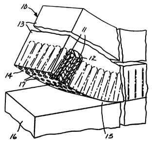
Referring to FIG. 1, composite article 10 comprises
a plurality of microstructures 11, optional conformal
coating material 12, and encapsulating material 13
partially broken away to show detail. Further, FIG. 1
illustrates delamination of composite article surface 14
from substrate surface 15 of substrate 16, exposing
distal ends of microstructure 17.
The thickness of the overcoating (i.e., encapsulant)
is typically in the range from about 1 micrometer to
about 1 mm, depending on the particular application.
Methods for depositing an overcoating material on
the delaminated surface of the composite article of the
present invention include techniques known in the art for
depositing the coating material on a substrate. Such
methods include, for example, the methods described above
for depositing the conformal coating on the
microstructured surface and the methods described above
for depositing the encapsulating material onto the
microstructured-layer or conformal-coated,
microstructured-layer.
It is in the scope of the present invention to have
WO 93/0(156a PCT/US92/04512
21 10485
- 24
a composite article having multiple microstructured-
layers. For example, two or more composite articles may
be laminated together.
The composite article of the present invention is
useful for visible radiation absorbing devices, such as,
for example, selective solar absorbers, flat plate solar
collectors, solar absorption panels (such as the type of
devices described in U.S. Pat. No. 4,148,294) and solar
cells (such as the type of device described in U.S. Pat.
No. 4,155,781).
Objects and advantages of this invention are further
illustrated by the following examples, but the particular
materials and amounts thereof recited in these examples,
as well as other conditions and details, should not be
construed to unduly limit this invention. All parts and
percentages are by weight unless otherwise indicated.
Example 1
A sample was prepared by spraying a latex rubber
onto a microstructured-layer of discrete, perpendicularly
oriented crystalline whiskers, comprising
N,N'-di(3,5-xylyl)perylene-3,4,9,10 bis(dicarboximide)
(i.e., perylene red), prepared using the techniques
described in U.S. Patent No. 4,812,352. Specifically, a
layer of copper having a thickness of about 100
nanometers was deposited onto a glass microscope slide by
sputtering. N,N'-di(3,5-xylyl)perylene-3,4,9,10
bis(dicarboximide), an organic pigment commercially
available under the trade designation "C.I. PIGMENT RED
149" from American Hoechst Corp, of Somerset, NJ, was
vacuum vapor deposited ("base" pressure of about 2 X 10~
Torr) onto the copper-coated microscope slide to a
thickness of about 146 nm at an average deposition rate
of 20 nm/minute.
The resulting composite was then annealed to a
maximum temperature of 200°C in a vacuum to convert the
WO 93/00560 P~"T/US92/04512
~21 10485
- 25 -
organic layer to a microstructured-layer of discrete,
perpendicularly-oriented crystalline whiskers.
Approximately one-third of the microstructured-layer
was sputter coated with copper to provide a conformal
copper coating.having an equivalent planar thickness of
about 100 nanometers. The effective thickness of the
copper coating on the sides of the whiskers was
significantly less than 100 manometers due to the much
larger surface area of the whiskers relative to a flat
surface.
About one-half of the microstructured-layer was
sputter-coated with platinum to provide a conformal
platinum coating having an equivalent planar thickness of
about 100 manometers.
The remaining one-sixth of the microstructured layer
was left uncoated.
A conventional air pressurized spray painter was
used to spray a layer of an encapsulating precursor
(commercially available under the trade designation
"STRIPPABLE MASKANT YR-43" from the 3M Company of St.
Paul, MN) over the entire microstructured-layer to
provide a wet thickness of about 0.157 to about 0.165 mm.
The encapsulating layer was dried in a conventional oven
at about 6 6°C ( 15 0°F ) f or about 2 0 minutes .
The resulting composite article on the copper-coated
glass slide (i.e., the conformal-coated microstructured-
layer with the encapsulating material coated thereon) was
cut into strips about 0.6 cm (0.25 inch) wide with a
razor blade. The composite layer of each strip
comprising the conformal-coated and uncoated (i.e., the
portion of the microstructured layer not having the
copper or platinum conformal coating) microstructured-
layer and the encapsulating material was delaminated from
the surface of the copper-coated glass slide. The
relative adhesion of the areas of the composite having
the copper conformal coating, the platinum conformal
coating, and no conformal coating (i.e., bare whiskers),
WO 93/00560 PCT/US92/04512
2l 10485
- 26 -
to the copper-coated glass slide were observed to be
different. Adhesion of the strips having platinum as the
conformal coating to the copper-coated glass surface was
the greatest, followed by the adhesion of the strips with
conformal copper coating to the copper-coated surface.
The weakest adhesion observed was that of the strip
having bare whiskers to the copper-coated surface.
Delamination of the composite layers having the
conformal platinum coating, the conformal copper coating,
and the bare whiskers from the copper-coated glass
surface was observed to be 100%.
A SEM of the delaminated surface of the composite
layer taken at about 2000X revealed that the whiskers
protruded slightly from the latex encapsulant.
Examgle 2
Conventional aluminum foil having a thickness of
about 0.025 mm (0.001 inch) was stretch-mounted between
two stainless rings each having a diameter of about ten
centimeters. One surface of both the aluminum foil and
the rings were cleaned by vapor degreasing and oxygen
plasma etching.
A microstructured-layer of whiskers comprising
perylene red was deposited onto the "cleaned" aluminum
surface and the stainless steel rings using the method
described in Example 1 for forming the microstructured-
layer onto the copper-coated glass surface.
The microstructured-layer on the foil and rings was
sputter-coated with CoCr to provide a conformal CoCr
coating having an equivalent planar thickness of about
125 nanometers. The sputter coating was done using a
conventional rf (13.7 I~iz) glow discharge unit, wherein
the distance between the twenty centimeter (8 inch)-
diameter targets and the substrate was about ten
centimeters. The sputtering pressure was about 24 mTorr
of Ar, forward power was about 500 watts, and target bias
was about 1200 volts. The substrate support was water
WO 93/00560 p~'T/US92/04512
-2 ~ 10485
- 2~ -
cooled during the sputtering of the CoCr.
Several droplets of an adhesive, i.e., a solution of
a thermoplastic resin in toluene or other solvents,
(commercially available under the trade designation "DUCO
CEMENT" from Devcon Corp. of Wood Dale, IL) were placed
on the perimeter of one of the stainless steel rings,
giving about a 90 degree contact angle at the
adhesive-conformal-coated microstructured-layer
interface. The droplets were covered with several small
pieces (about lcm x icm) of 152 micrometer (6 mil) thick
polyester film to slightly spread each droplet of cement
over an area about 6 to 9 mm in diameter. The adhesive
was partially dried in air for about 10 minutes and then
heated at about 50°C for about 2 hours. The patches of
dried adhesive having conformal-coated whiskers bonded
thereto, were easily delaminated from the stainless steel
ring by sliding the edge of a razor blade under each
patch to form self-supporting petals having a thickness
of about 0.1 to about 0.125 mm.
A SEM of a freeze fractured edge of one of the
delaminated composites having the CoCr conformal coating,
taken at about 10,000X, revealed that the whiskers
appeared to be oriented with one end located at the place
of the original interface with the stainless steel
substrate. Further, it appeared that the relief of the
delaminated surface was a "negative" of the surface
texture of the stainless steel ring.
The delaminated composite layer (article) had
sufficient integrity to be handled, rubbed, bent, and
stretched with no apparent degradation in its physical
characteristics.
The composite layer was observed to be attracted to
a small hand held magnet.
Example 3
A piece of conventional aluminum foil (about 25
micrometers thick) was stretch-mounted on an 8.9 cm
WO 93/00560 PCT/US92/04512
21w10485
- 28
diameter stainless steel ring. A surface of the aluminum
foil was cleaned as described in Example 2. A
microstructured-layer of perylene red was deposited onto
the "clean" aluminum surface by the method described in
Example 1.
The microstructured-layer was sputter-coated with Fe
to provide a conformal Fe coating having a planar
thickness of 280 nm. The conformal-coated
microstructured-layer was then overcoated with a layer of
adhesive ("DUCO CEMENT") by applying several drops of the
adhesive to the center of the coated aluminum foil and
then spinning the coated aluminum foil for about 5 to 10
seconds at about 500 rpm. The amount of adhesive used
was sufficient to provide a cured thickness of about
0.064 mm. The resulting composite layer, which comprised
the conformal-coated microstructured-layer and the
adhesive, was easily delaminated from the aluminum foil
surface. However, delamination required more force than
in Examples 1 and 2. Delamination appeared to be 100%.
FIG. 2 (a) shows a SEM of the delaminated surface of
the composite layer at a viewing angle of about 45
degrees to the surface normal at 10,000X. FIG. 2 (b)
shows a SEM of an edge view of the delaminated surface of
the composite layer at 15,000X.
Example 4
A microstructured-layer of perylene red was
deposited onto aluminum foil as described in Example 3.
The microstructured-layer was sputter-coated with copper
to provide a conformal coating of copper having a planar
equivalent thickness of about 100 nm.
A polyester resin (commercially available under the
trade designation "VITEL 200A" from Goodyear Tire and
Rubber Co. of Atlanta, GA) was blended with a solvent
containing equal portions of methyl ethyl ketone and
toluene to provide an encapsulating resin having about 45
percent solids. The encapsulating resin was overcoated
WO 93/00560 ?CT/US92/04512
.. . ~ 2~1 10485
- 29 -
onto the conformal-coated microstructured-layer by
applying drops of the resin to the layer, which flowed to
about 1 cm diameter areas. The encapsulating material
was then allowed to air dry. The thickness of the dried
encapsulating resin was about 0.25 mm. The resulting
composite layer comprising the conformal-coated
microstructured-layer and the encapsulating material was
delaminated from the aluminum foil surface by peeling the
aluminum foil away from the composite layer. Delamin
l0 ation appeared to be 100%.
Example 5
The (delaminated) composite layer of Example 5 was
prepared as described in Example 4 except the
encapsulating material was a rubber adhesive resin
(commercially available under the trade designation
"ADHESIVE 847" from the 3M Company) and the adhesive was
cured by air drying at room temperature.
Delamination of the composite layer appeared to be
100%, although delamination was somewhat more difficult
than for the more rigid composite layers described in
Examples 2, 3, 4, 7, 8, 9, 10, 11, and 14.
Example 6
A polyimide film (commercially available under the
trade designation "NOVAL" from Mitsubishi Chemical
Industries Ltd. of Tokyo, Japan) having a thickness of
0.05 mm (2 mils) was stretch-mounted in stainless steel
rings, to form an 8.9 mm diameter disc, cleaned (as
described in Example 2) and sputter-coated with about a
100 nm layer of copper (as described in Example 4). A
microstructured-layer of perylene red was formed onto the
copper-coated surface as described in Example 1. The
microstructured-layer was then sputtered coated with Fe
to provide a conformal coating of Fe having a planar
equivalent thickness of about 210 nm.
Three milliliters of adhesive ("DUCO CEMENT") were
WO 93/00560 PCT/US92/04512
21 10485
- 30 -
uniformly applied to the 8.9 diameter disc by spin
coating at about 560 rpm for about 3 seconds. The
adhesive was allowed to air dry at room temperature. The
copper-coated polyimide film was easily peeled away from
the resulting composite layer comprising the
conformal-coated microstructured-layer and the adhesive.
Examples 7-11
Examples 7-il illustrate the use of radiation
curable materials as encapsulants.
Example 7
Several drops of a W curable optical adhesive
(commercially available under the trade designation "NOA
68" from Norland Products, Inc. of New Brunswick, NJ)
were applied to a CoCr-coated microstructured-layer of
perylene red prepared as described in Example 2. Each
drop of adhesive was allowed to wet out to its
self-determined thickness. The adhesive was cured in a
flowing nitrogen atmosphere under W lamps (commercially
available under the trade designation "LIGHTCAST II" from
Merck, Sharp & Dohme Orthopedics, Co. of West Point, PA)
for about 1 hour. The resulting composite comprising the
adhesive and the CoCr-coated microstructured-layer were
delaminated from the aluminum foil. Delamination
appeared to be about 100%.
Thickness of the composite layer varied from about
0.125 to about 0.875 mm.
A SEM of a freeze fracture prepared sample of the
composite layer taken at a 45 degree angle at about
15,OOOX showed that the microstructured-layer was
embedded at the surface of the composite layer,
essentially perpendicular to the original substrate
(i.e., aluminum foil) interface.
Example 8
A CoCr-coated microstructured-layer of perylene red
was prepared as described in Example 2. About 0.5 ml of
WO 93/00560 PCT/US92/04512
.. . 2110485
- 31 -
an uncured photopolymer comprising one part cyclohexyl
methacrylate (commercially available under the
trademarked designation "SARTOMER 208 MONOMER" from
Sartomer Co., Inc. of Westchester, PA) to one part of a
casting composition prepared as disclosed in Example 11
of U.S. Pat. No. 4,785,064, except that one mole of
pentaerythritol triacrylate and two moles of 2-
hydroxyethyl methacrylate were used instead of the two
moles of pentaerythritol triacrylate and one mole of 2-
hydroxyethyl methacrylate, photopolymer, were spin-coated
at about 950 rpm onto a triangular shaped piece (2.5 cm
long sides) of the CoCr-coated microstructured-layer.
The photopolymer was cured as described in Example 7 for
about 30 minutes. The resulting composite layer
comprising the cured photopolymer and the CoCr-coated
microstructured-layer was separated from the aluminum
foil by immersing the composite layer-substrate in liquid
nitrogen and then peeling the composite away.
Delamination appeared to be 100%.
The delaminated surface of the composite layer was
metallic-green. The opposite side of the composite layer
(i.e., the cured photopolymer) was shiny and black.
Example 9
A microstructured-layer of perylene red was formed
on a copper-coated polyimide film as described in Example
6. The microstructured-layer was sputter-coated with
CoCr as described in Example 2 to provide a conformal
CoCr coating having an equivalent planar thickness of
about 125 nanometers. An uncured photopolymer
(described in Example 8, above) was coated onto the
microstructured-layer, cured, and the resulting composite
layer delaminated as described in Example 8. Again,
delamination appeared to be 100%.
Example 10
A microstructured-layer of perylene red having a
WO 93/00560 PCT/US92/04512
2110485
- 32 -
conformal coating of Fe was prepared as described in
Example 3. About 6 ml of a photopolymer (prepared as
described in Example 6 of U.S. Pat. No. 4,510,593) were
poured onto the conformal-coated microstructured-layer
and gently rocked to cause the photopolymer to uniformly
distribute itself over the sample. The photopolymer was
cured as described in Example 7 for about 30 minutes.
The aluminum foil was easily peeled away from the
resulting composite layer comprising the conformal-coated
microstructured-layer and the cured photopolymer.
Delamination of the microstructured-layer from the
aluminum foil appeared to be 100%.
Example 11
A microstructured-layer of perylene red having a
conformal coating (250 manometer planar equivalent
thickness) of CoCr was prepared as described in Example
9. A photopolymer (prepared as described in Examples 1
and 2 of U.S. Pat. No. 4,262,072) was applied to the
conformal-coated microstructured-layer and cured as
described in Example 10.
The composite layer comprising the conformal-coated
microstructured-layer and the cured photopolymer was
delaminated from the copper-coated polyimide film as
follows. About 5 ml of an acid-based UV curable
adhesive, comprising 90% isooctyl acrylate at 10% acrylic
acid (prepared as described for composition 1 in Examples
1-17 of U.S. Pat. No. 4,181,752) was blended with about
0.27 percent by weight of 1,6-hexanediol diacrylate
(based on the weight of the 5 ml of the acid-based UV
curable adhesive) and about 0.2 percent by weight of 2,2-
dimethoxy-2-phenylacetophenone (commercially available
under the trademarked designation "IRGACURE" from Ciba-
Geigy Corp. of Summit, N.J.), and applied to the exposed
surface of the cured photopolymer in a circular stripe
midway between the center and edge of the sample. A 15
cm diameter piece of surface primed polyester having a
WO 93/00560 PCT/US92/04512
.: 2,~ ~ p~485
- 33 -
thickness of 0.1 mm was placed primed side down onto the
adhesive-coated surface of the composite. The polyester
film was flattened to distribute the adhesive evenly over
the exposed surface of the composite layer. The adhesive
was UV cured for 55 minutes as described in Example 7.
The resulting composite comprising the conformal-coated
microstructured-layer, the cured photopolymer, the cured
acid-based photocurable prepolymer adhesive, and the
surface primed polyester were delaminated from the
l0 copper-coated polyimide film. Delamination appeared to
be 100%.
Example 12
A microstructured-layer of perylene red was
deposited onto an 8.9 cm diameter polished steel disc
electroplated with nickel, using the method described in
Example 1 for depositing a microstructured-layer onto
copper-coated glass. The microstructured-layer was
sputter-coated with CoCr as described in Example 2 to
provide a conformal coating of CoCr having an equivalent
planar thickness of 200 nm.
A thin layer of a polymer (prepared as disclosed in
Example 4 of U.S. Pat. No. 4,986,496) was applied to the
conformal-coated surface by spin coating about 1.5 ml of
the photopolymer at about 3000 rpm for about 1 minute.
The photopolymer was UV cured in flowing nitrogen gas for
about 30 minutes using the W lamps described in Example
7. The composite layer comprising the conformal-coated
microstructured-layer and cured photopolymer was
delaminated from the nickel-plated disc using the
delamination technique described in Example 11.
Delamination appeared to be 100%.
Example 13
A microstructured-layer of perylene red was
deposited on aluminum foil as described in Example 2,
except the organic layer comprising perylene red was
WO 93/00560 PCT/US92/04512
21 10485 - 34 -
coated onto the aluminum foil maintained at about 200°C at
a rate of about 0.25 nm/second and the organic layer was
not annealed after it was coated onto the aluminum foil.
The resulting microstructured-layer comprised randomly
oriented whiskers which were larger in size than the
whiskers comprising the microstructured-layer of Example
2.
The microstructured-layer was sputter-coated with
CoCr as described in Example 2 to provide a conformal
coating of CoCr having an equivalent planar thickness of
about 125nm.
About 3 drops of the W curable adhesive described
in Example 11 were applied to a 2.5 cm X 2.5 cm area of
the conformal-coated microstructured-layer. The W
curable adhesive was distributed over the
microstructured-layer by using a piece of polyester as
described in Example 11. The W curable adhesive was
cured for about 20 minutes in flowing nitrogen gas using
the W lamps as described in Example 7.
The resulting composite layer comprising the
conformal-coated microstructured-layer and the cured UV
adhesive was delaminated from the polyester substrate by
peeling the polyester away from the composite layer.
Delamination appeared to be 100%.
Example 14
A conformal-coated microstructured-layer was
prepared as described in Example 2. The
microstructured-layer of perylene red was sputter-coated
with copper using the system described in Example 2 to
provide a conformal coating of copper having an
equivalent planar thickness of about 60nm.
The conformal-coated microstructured-layer was
coated with two drops of a two part epoxy (commercially
available under the trade designation "5-MINUTE EPOXY"
from Devcon Corp.) The epoxy was spread over the
microstructured surface by hand.
WO 93/00560 "CT/US92/04512
2 t 10485
- 35 -
The epoxy was 'allowed to cure in air at room
temperature overnight. The resulting composite
comprising the conformal-coated microstructured-layer and
cured epoxy were delaminated from the aluminum foil by
peeling the aluminum foil away from the composite layer.
Delamination appeared to be 100%.
Example 15
A microstructured-layer of perylene red was
deposited onto a 9.5 cm diameter nickel-plated disc as
described in Example 12. The microstructured-layer was
sputter-coated with CoCr as described in Example 2 to
provide a conformal coating of CoCr having an equivalent
planar thickness of about 70 nm.
The nickel-plated disc having the conformal-coated
microstructured-layer thereon was placed microstructured
layer side up in a 154 cm diameter glass dish and
covered. The covered dish was heated to about 158°C on a
hot plate with a flow of nitrogen gas passing through the
covered dish.
When the temperature of the disc reached about 158°C,
about 50 cubic pellets (3 to 4 mm per side) of a
polyester material (commercially available under the
trade designation "VITEL PE200 POLYESTER" from Goodyear
Tire and Rubber Co. of Atlanta, GA) were placed on the
conformal- coated microstructured-layer. The polyester
pellets melted into a pool approximately 3.5 cm in
diameter. The disc was allowed to cool in air during
which time the liquified polyester solidified. The
resulting composite layer comprising the conformal-coated
microstructured-layer and the solidified polyester
overcoat were easily delaminated from the nickel-plated
substrate by inserting a razor blade at the
disc-microstructured-layer interface. The delaminated
surface of the composite layer had a mirror-like
metallic-bronze finish. Delamination appeared to be
WO 93/00560 PCT/US92/04512
2110485
- 36 -
100%.
Example 16
A composite disc was prepared as described in
Example 15 except about 18 small pellets, 2 to 4 mm per
side, of bis phenol A polycarbonate were used in place of
the polyester pellets, and liquification of the pellets
was accomplished by heating the disc to about 200°C. The
liquefied bis phenol A polycarbonate solidified upon
cooling. Delamination appeared to be 100%. The
resulting composite layer provided a structure comprising
conformal-coated microstructured-layer and solidified bis
phenol A polycarbonate.
Example 17
A composite disc was prepared as described in
Example 15 except about 4 or 5 cubic pellets of a
polycarbonate (commercially available under the trade
designation "LEXAN 123-112 POLYCARBONATE" from General
Electric of Cleveland, OH) were used in place of the
polyester pellets, and liquification of the pellets was
accomplished by heating the disc to about 200°C. The
liquefied polycarbonate solidified upon cooling.
Delamination of the resulting composite layer provided a
structure comprising a conformal-coated
microstructured-layer and solidified polycarbonate.
Delamination appeared to be 100%.
Example 18
A composite disc was prepared as described in
Example 15 except about 4 or 5 cubic pellets of
poly(methylmethacrylate) were used in place of the
polyester pellets, and liquification of the pellets was
accomplished by heating the disc to about 200°C. The
liquefied poly (methylmethacrylate) solidified upon
cooling. Delamination of the resulting composite layer
WO 93/00560 ~('T/US92/04512
a .2 ~ ~.,p485
- 37 -
provided a structure comprising a conformal-coated
microstructured-layer and solidified
poly(methylmethacrylate). Delamination appeared to be
100%.
Example 19
This example illustrates the radiation absorbing
ability of a composite article according to the present
invention.
A microstructured-layer of perylene red was
deposited orrtio~ ~ a copper coated polyimide film as
described in Example 6. The microstructured-layer was
vacuum vapor-coated with gold to provide a conformal
coating of gold having a planar equivalent thickness of
about 2500 nm.
An adhesive ("DUCO CEMENT") was applied to the
conformal-coated, microstructured-layer as described in
Example 6 to provide a composite cured thickness of about
0.06 mm.
The copper-coated polyimide film was easily peeled
away from the resulting composite layer comprising the
conformal-coated microstructured-layer and the adhesive.
The absolute reflectance and transmittance spectra
of the delaminated composite layer were measured using a
conventional UV-visible spectrophotometer over the
wavelength range from 200 to 800 nm. The reflectance
measurements were made in the specular mode (i.e., the
angle of reflectance equals the angle of incidence),
about 5 degrees off normal incidence. The transmission
measurements were made with the composite article in
close proximity to an integrating sphere so that there
was an included angle for the detector of about 60
degrees from the normal to the delaminated surface of the
composite layer. The measured reflectance was less than
or equal to about 1.6% over the 200 to 800 nm wavelength
range. The measured transmittance was less than or equal
to about 0.3% over the 200 to 800 nm wavelength range.
WO 93/00560 PCT/US92/04512
2110485
- 38 -
The results show that the composite layer absorbs over
98% of incident radiation having a wavelength in the
range from about 200 to about 800 nm.
Various modifications and alterations of this
invention will become apparent to those skilled in the
art without departing from the scope and spirit of this
invention, and it should be understood that this
invention is not to be unduly limited to the illustrative
embodiments set forth herein.