Note: Descriptions are shown in the official language in which they were submitted.
WO 92/22192 PCI/EP92/01133
2110679
METHOD OF MANUFACTURING A MULTILAYER PRINTED WIRE BOARD
The invention relates to a method of manufacturing a multilayer
printed wire board. Such a printed wire board comprises at least three
conductive layers, of which usually at least two layers are copper-
layers on the outer surfaces and at least one layer is an internal
circuit. The method to which the invention pertains comprises bonding
by lamination at least one hard base substrate which is provided with
conductive traces on both sides and at least one intermediate
substrate which comprises a hard core layer provided with an adhesive
layer at least at the side facing the conductive traces of the base
substrate.
Such a method has been disclosed in IBM Technical Disclosure Bulletin
Vol 32 No. SB, pages 355-356, and serves to substantially eliminate
the dimensional instability that usually occurs in composite
lamination processes. While this can be recognized as a substantial
improvement in the manufacture of multilayer boards, the disclosure
fails to address an even more important problem associated with
multilayer boards, viz. that of providing a material displaying
thermal coefficients of expansion (TCE) sufficiently low so as to
match the TCE of electronic components (chips) used in conjunction
with the multilayer board. A woven glass fabric (cloth) being used as
the reinforcement material it is immediately apparent to the person of
ordinary skill in the art that the TCEs obtained are relatively high.
Further, the prior art substrates and the resulting multilayer boards
require improved dimension stability.
Similar considerations apply to US 3,756,891, which discloses a method
of manufacturing multilayer PWBs involving the stacking of circuitized
boards wlth adhesive coated sheets. The adhesive is chosen so as not
to flow into the through-hole interconnection areas present in the
boards.
WO 92/22192 PCI'/EP92/01133
211067~
A different approach towards multilayer PWBs is the sequential
laminating technique disclosed in RCA review 29 (1968) pages 582-599,
particularly pages 596-597. Although a base-substrate provided with
circuitry on both sides is laminated with an adhesive coated
dielectric layert the adhesive coated layer is not an intermediate
substrate in between base substrates in accordance with the invention,
but serves as a substrate for a next printed circuit. The disclosure
does not address the type of substrate used, let alone that it can
provide a solution to the problem of providing multilayer boards
having sufficiently low TCEs.
PWBs providing advantages with respect to TCE have been disclosed in
- US 4 943 334. Described is a manufacturing process which comprises
winding reinforcing filaments about a square flat mandrel to form a
plurality of layers of filaments intersecting at an angle of 90,
providing the plurality of layers with a curable matrix material, and
curing the matrix so as to form a base material for a PWB. In order to
provide multilayer PWBs the disclosure teaches a method comprising
providing an assembly of PWBs in a cavity, introducing a curable
matrix material into the cavity, and curing the matrix so as to form a
multilayer PWB. The desired reinforcement of the matrix is.obtained by
the presençe of fibres around the PWBs, which during the process will
become embedded in the cured matrix. The method fails to provide
acceptable suitable results due to, inter alia, an.internal lack of
thickness-tolerance.
In C.J. Coombs, jr.'s Printed Circuits Handbook, published by
Mc6raw-Hill, chapters 31 and 32, more particularly 33 and 34, it is
described, int. al., how a multiple layer printed wire board, a so-
.called multilayer, is generally manufactured, the process being
comprised of the following steps:
- manufacturing a laminate coated on both sides with copper foil
from glass fabric-epoxy prepreg;
- etching the desired pattern into the copper;
wo g2/22lg2 2 1 1 ~ ~ 7 3 PCI /EP92/01133
- bonding the etched laminates by pressing them together with
intermediate layers of glass fibre-epoxy prepreg.
There are a number of drawbacks to this process, such 'as high
materials costs on account of glass fabric being employed and high
thermal expansion on account of the low maximum fibre content in
fibre-reinforced laminates. Another major drawback to this process is
that there is no absolute thickness tolerance. The thickness of a
multilayer formed in this manner is dependent on, int. al., the
moulding pressure exerted, the moulding temperature and the warming-up
- rate employed, and the "age" of the used prepreg and some ~ther
factors which are hard to control.
There are several variations from the latter process, e.g., as
disclosed in EP 0 231 737 A2. In this known process a multilayer
printed wire board is manufactured in a continuous process. In the
embodiment according to Fig. 2 of this publication use is made of a
'single printed wire board (PWB) comprise~ of a substrate of two layers
of glass cloth in a cured matrix of thenmosetting synthetic material,
which substrate is provided on both sides with a layer of copper
traces formed by the subtractive method from the copper foil
originally applied' to the substrate. To this initial PWB there are
applied, on-'both sides, two layers of glass cloth, a layer of liquid
thermosetting material, such as epoxy resin. and a copper foil. After
preheat~ng the whole is laminated in a double belt press under the
effect of heat and pressure. Thus, after cooling as it leaves the
double belt press, a laminate is obtained which after the forming of
copper traces in the outer layers makes a multilayer PWB. Hence this
multilayer PWB is made up of a laminate of three substrates of glass
cloth-reinforced cured epoxy resin and four layers with copper traces.
Although quite reasonable results can be obtained using the multilayer
PWB manufactured according to this known process, it still has certain
drawbacks. Notably, the layers of liquid, not yet cured thermosetting
W092~22192 . PCI/EP92/Olt33
21~ ~79
resin are greatly pressed together in the double belt press, as a
result of which there is a substantial decrease of the laminate's
thickness between the double belt press's inlet and its outlet. It has
been found that as a result of this major change in thickness it is
hard to maintain with sufficient accuracy the constant thickness of
the finished laminate and of the finished multilayer PWB as ultimately
desired. Deviations in a PWB's thickness have an unfavourable effect
on its electrical properties, thus negatively affecting the quality of
such a PWB. Another drawback to said known multilayer PWB is that
reinforcing the substrates with fabrics is a comparatively costly
affair.
DE-4 007 558 Al describes a multilayer PWB of a somewhat different
type. Between a number of adjacent single PWBs (cf. Fig. 1, no. 2 of
DE-4 007 558 Al) which are each composed of a substrate (cf. Fig. 1,
no. 4) made up of a glass cloth impregnated with a thermosetting
synthetic material and provided on both sides with copper traces (cf.
Fig. 1, no. 5), there is interposed in each case a sort of
intenmediate substrate (Fig. 1, nos. 1-a and 1-b). ~he intermediate
substrate (1) consists in this case of a polyimide film (1-a) of a
thickness of 10 ym which is provided on both sides with an adhesive
layer (1-b) of a thickness of 10 ym or less. The melting ~temperature
of the polyimide film is higher than the temperature used during
lamination, while the adhesive layers have a melting temperature below
the used lamination temperature.
A disadvantage of said known multilayer PWB consists in that there is
- air in the voids between the copper traces (cf. Fig. 1), which may
have àn unfavourable`effect on the properties. Other disadvantages of
DE-4 007 558 A1 include the high materials cost price of the described
constituents and the lengthy processing time required.
In US 4 606 787 a process for manufacturing a multilayer PWB is
described which comprises first (cf. Fig. 12) making a stack of a
wo 9~22lg2 2 1 1 3 ~ 7 9 PCI/EI'92/01133
number of single PWBs with sandwiched therebetween in each case a sort
of intermediate substrate of glass fibres impregnated with liquid,
uncured epoxy resin. Next, said stack is pressed together under
pressure and at elevated temperature, with the resin filling'the voids
between the conductive traces (cf. column 6, 11. 51, S2) and being
cured. The pressing together of the laminate gives a substantial
reduction of its thickness, making it difficult to maintain with
sufficient accuracy the constant overall thickness of the finished
~ laminate as ultimately desired and the constant thickness of the
individual intermediate substrates. This has an unfavourable effect on
the PWB's elëctrical properties, thus negatively affecting its
quality.
- The invention has for its object to provide a method in which said
drawbacks have been obviated. The process according to the invention
consists therein that in a method of the known type referred to in the
opening paragraph the adhesive layer is flowable and lamination is
condùcted under a pressure sufficiently high so as to bring the core
layer of the intermediate substrate into contact or virtually into
contact with the conductive traces of the base substrate, the adhesive
filling the voids between the traces, the base substrate and the
intermediate substrate comprising a fibre-reinforced matrix material,
the reinforcement being in the form of a crosswise arrangement of
layers of unidirectionally (UD) oriented fibres~ A flowable adhesive
' génerally is an adhesive which either is fluid or can be rendered
fluid (ùsually'by means of elevated temperature).
. - . .
Thus,~according to the invention, for the hard core layer of the
intermediate' substrate and as the hard base-substrate there is
employed a reinforced matrix material which obviates the afore-
mentioned drawbacks and notably has a sufficiently low TCE and
advantageous flatness. This material comprises two or more layers of
reinforcing fibres or filaments embedded in a cured thermosetting
synthetic material based on, e.g., epoxy resin. The reinforcement is
WO 92~221g2 PCI`/EP92/01133
2110~7~
in the form of filament-containing layers composed of a plurality of
mutually parallel stretched filaments not bound in the form of a
fabric and extending substantially rectilinearly, and with filaments
of superposed layers crossing each other. This type of reinforced
matrix material is referred to as UD-reinforced material for short.
According to the invention preferably three of said filament layers
not bound in the form of a fabric are arranged in the matrix material
in mirror image relative to the plane of symmetry in this process,
with the filaments of superposed filament layers crossing at an angle
of preferably about 90. This UD-reinforced material, more accurately
referred to as a cross-ply of UD-reinforced layers, to be suitable for
advantageous use in multilayer PW8s is balanced and mid-plane
symmetric. An example of such a material is formed by the substrates
- disclosed in the afore-mentioned US 4,943,334. By virtue of the
lamination method according to the invention, making use of a flowable
adhesive which is not substantially present between the conductive
traces of a base-substrate and the hard core of an adjacent
intermediate substrate, the advantages of UD-reinforced material can
be employed in a multilayer PWB.
These advantages particulàrly include a favourable dimension
stability. Further the substrates used have relatively low ~CEs in the
X and Y directions, preferably about equal to those of ~the
electrically conductive material employed (usually copper). Further,
it is possible` to provide substrates having coefficients of expansion
in the X and Y directions about equal to the coefficient of expansion
of eiectronic components to be used in conjunction with the multilayer
PWB, more particularly silicon chips. It should be noted that these
components can be ~applied either onto the multilayer board
(Uchip-on-board'')l or can be embedded in a substrate such as an
intermediate substrate in accordance with the present invention
("chip-in-board"). With regard to the latter embodiment an adhesive-
coated substrate should be provided with open spaces for embedding the
chips. Of course, it is also possible to embed the chips in spaces
wo 92l22192 211 0 G 79 F~r/EPg2/01133
provided in a base-substrate. An advantageous method to manufacture a
~chip-in-boardU structure includes placing one or more chips on a
base-substrate (and connecting it conductively with the circuitry on
the base-substrate), and then laminating onto the chip-containing
base-substrate an adhesive-coated intermediate substrate provided with
appropriate spaces so as to surround the chip or chips attached to the
base-substrate.
A particularly effective embodiment of the process according to the
invention is characterised in that use is made of an intermediate
substrate which is provided on both sides of the hard core layer with
the flowable adhesive layer. According to the invention in this case
the intermediate substrate can be simply sandwiched between two
' adjacent base substrates provided with conductive traces, and such
pressure is exerted on the laminite during the laminating process as
will bring said hard core layer of the intermediate substrate into
virtual contact with the conductive tra~es of the two base substrates
and `fill the ~oid between these traces on either side of the
intermediate substrate with the adhesive material. According to the
- 20 invention, a multilayer PWB having many layers can be easily realised
when each of n-l intermediate substrates (n ~ 2) is sandwiched
between, in each `case, n adjacent base substrates, rollowed by
laminati'on "-under increased pressure (and optionally increased
~ temperature), under vacuum, or under a combination of the two.
-~ 25
A'`favourable em~bodiment of the process according to the invention is
characterised in that~ the thickness of the hard core layer of each
intermediate substrate is 0,025-0,6 mm, although preferably the
thickness of each intermediate substrate is of the same order of
magnitude as that of a base substrate, and the thickness of each still
plastically deformable (flowable) adhesive layer on one or both sides
of the intermediate substrate is of the same order of magnitude as
that of the conductive traces, which generally have a thickness of
2-70 ~m. Preferably, the process according to the invention is
WO 92122192 PCI/EP92/01133
2110~9 8
characterised in that for the flowable adhesive layer provided on one
or both sides of an intermediate substrate's hard care layer use is
made of a glue based on a still uncured or only partially cured
thermosetting synthetic material, such as epoxy resin, whic~ is cured
after the voids between the conductive traces have been filled.
The invention will be further illustrated with reference to the
schematic drawing. Shown in Fig. 1 is the manufacture of a single PWB
by means of the subtractive method. Figs. 2-7 show the manufacture by
the subtractive method of a PWB having six layers of copper traces.
Shown in Fig. 8 is the manufacture of a known single PWB by means of
the additive method. Figs. 9-12 show the manufacture by the additive
method of a PWB having six layers of copper traces. Figs. 13-16
- illustrate another procedure for the manufacture of a PW8 having four
or six layers of copper traces.
Fig. 1 shows a substrate 1, the outer sides of which are composed of a
continuous copper foil 2 fixedly provided thereon. The core 3 of the
substrate 1 is composed of a matrix 4 of a cured thermosetting
synthetic material based on epoxy resin, which is reinforced with
three layers of stretched filaments not bound in the form of a fabric
and extending rectilinearly, with the combined thickness of the two
~ outer iayers being equal or virtually equal to the thickness of the
- centre layer. The two outer filament layers ~ are indicated with dash
lines and the filaments in these layers extend mutually parallelly and
parallel to the plane of the drawing (0 direction). The inner
filament layer 6 is indicated with dotted lines and extends at right
angles to the plane of the drawing (90 direction). In effect, the
core 3, the thickness of which is, say, 0,4 mm, of the substrate 1 is
made of layers of mutually parallel (unidirectional - UD) reinforcing
filaments impregnated with a thermosetting material, such as epoxy
resin. Next, the desired copper traces 7 having a thickness of, say,
35 ~m, are formed in the copper foils by an etching process, i.e., by
the subtractive method, after which the base substrate indicated in
its entirety with 8 is finished.
w o 9v~21s2 211 ~ 6 7 ~ PCI~/EPg2/01133
As will be illustrated in greater detail with reference to Figs. 2-7,
said base substrate 8, which in itself is a single PWB with two layers
of copper traces, forms a building component for the manufacture of a
multilayer PWB. ~o this end an intermediate substrate indicated in its
entirety with 9 is applied to either side of the base substrate 8 in
the manner indicated in Fig. 2. Each intermediate substrate 9 is made
up of a hard core layer 10, which has a matrix 11 of a cured
thermosetting resin, e.g. based on epoxy resin. The matrix 11 is
reinforced with at least two unidirectional layers of reinforcing
fibres. The filaments in the outer layers 12 of reinforcing fibres
- extend in the aforementioned 0 direction, while the filaments in the
inner layers 13 of reinforcing fibres extend in the aforementioned 90
direction. The core 10 of the intermediate substrate 9~ like the core
3 of the base substrate 8, is manufactured by laminating at least two
layers reinforced with virtually unidirectional fibres, giving a hard
core layer 10 with a thickness of, say, 0,4 mm. To the one side of
each intermediate substrate 9 there is applied a copper foil 14 of a
thickness of 35 ~m. To the other side, i.e., the side facing the
copper traces 7 of the base substrate 8, of each of the intermediate
substrates 9 is applied a flowable adhesive layer 15 of a thickness of
35 ~m. The adhesive layer 15 is composed of a quality type of glue and
preferably an uncured epoxy resin or a partially cured epoxy resin.
Preferably, the adhesive layer in the situation drawn in Fig. 2 is not
sticky, so that the intermediate substrate can be handled without any
problem. Next, the two intermediate substrates 9 with the base
substrate 8 therebetween are stacked as indicated in Fig. 3, and
joined together into an integrated whole under the effect of elevated
temperature and external pressure. The pressing together of the stack
shown in fig. 3 is carried out under such a pressure as will bring the
- 30 hard core layer 10 of the intermediate substrate 9 wholly or virtually
into contact with the copper traces 7 of the base substrate and
completely fill the void between these traces with glue or adhesive
material 15. With the external pressure being maintained~ the stack
shown in Fig. 3 is subjected to such a temperature as will cure the
WO 92/22192 PCI~/EP92/Ott33
2~ ~0~79 lo
glue 15 based on, say, epoxy resin. After the glue has been cured, a
laminate 16 forming an integrated whole is obtained. Next, the outer
copper foils 14 of the laminate 16 are subjected to an etching process
according to the subtractive method to form the desired copper traces,
giving the multilayer PWB 17 shown in Fig. 4. The PWB 17 already has
four layers of copper traces.
Manufacturing a PWB with six layers of copper traces may be as
illustrated in Figs. 5-7. The members of such a PWB are indicated in
Fig. 5 and consist of the centrally located PWB 17 with on either side
thereof another intermediate substrate 9 of the type described
hereinbefore. In the manner indicated in Fig. 6 these three members
are subsequently combined to form a stack 18, which is joined together
- into an integrated whole under the effect of heat and pressure, in
analogous manner to that described with reference to Fig. 3. The outer
copper foils 14 of the laminate 18 are then subjected to an etching
process according to the subtractive method to form the desired copper
traces, giving the multilayer PWB 19 shown in Fig. 7. The PWB l9 has
six layers of copper traces.
Making use of the PW8 19 combined with two intermediate substrates 9,
a PWB of eight layers of copper traces (not shown) can be manufactured
in a manner analogoùs to that illustrated in Figs. 2-4 and Figs. 5-7.
Of course, it is also possible to manufacture a PWB with seven layers
of copper traces, by combining the ~ix-layer PWB 17 with an
intermediate substrate 9 on one side only. It will be obvious that the
principle described with reference to Figs. 2-4 and Figs. 5-7 permits
the manufacture of PWBs with a plurality, say 20, layers of copper
traces. To simplify the drawing the various layers of reinforcing
filaments have not been drawn in Figs. 3, 4, 6, and 7. Needless to
say, the number of layers of reinforcing filaments is not restricted
to that given in the drawing and more such layers can be used if
desired. Care should preferably be taken to ensure that in the final
PWB the number of layers of reinforcing filaments is disposed in
WO g2/22192 PCI/EP92/01133
; 2110~73
mirror image relative to the plane of symmetry. This means that
identical laminate layers are always disposed at even distance from
the central plane of the multilayer above and below it, identical in
this case standing for, of even thickness, with the same orientation,
and of the same composition.
Shown in Fig. 8 is a substrate 20, of which the outer sides in
contradistinction to the substrate of Fig. 1 have not been coated with
a copper foil. Otherwise. the construction of the substrate 20 and its
reinforcement with layers of reinforcing filaments is the same as for
the substrate 1. The difference between the substrates 20 and
further consists in that the plastics matrix of the substrate 20
contains a catalyst, e.g. pàlladium. As a result there can be formed
on the substrate 20 in a manner known in itself by the additivive
method the copper traces 21, after which the base substrate indicated
in its entirety with 22 is ready.
Figs. 9-11 show that a PWB 24 with, in all, four layers of copper
traces can also be manufactured by combining the base substrate 22
with two intermediate substrates 23. The process illustrated in Figs.
9-11 is virtually wholly ident~cal with the process of Figs. 2-4, the
principal difference being that the intermediate substra~e 23 in the
hard core layer 25 contain a catalyst and have no copper foil coating.
The side of the intermediate substrate 23 facing the base substrates
îs again provided with a flowable adhesive layer 26, which is made up
of a quality type of glue. In a manner analogous to that described for
the laminate 16 of Fig. 3, the combination of layers shown in Fig. 9
is joined together under the effect of heat and pressure into an
integral whole to form the laminate 27 shown in Fig. 10. Next, copper
traces are applied to the outer sides of the intermediate substrates
in the laminate 27 by the additive method, giving the finished
multilayer PWB 24, which has four layers of copper traces.
WO 92/221g2 PCI~/EP92/01133
211067~
By being combined with two intermediate substrates 23 in the manner
indicated in Fig. 12, the PWB 24 in its turn may serve as a building
component for a PWB with six layers of copper traces, if desired.
Subsequently, the corresponding process steps described with reference
to Figs. 10 and 11 have to be carried out.
Figs. 13-16 illustrate a somewhat different process for the
manufacture of a multilayer PWB according to the invention. As is
indicated in Fig. 13, use is made in this case of two double-sided
PWBs 28 or base substrates, which each contain two layers of copper
traces 29 provided by the subtractive method or the additive method.
The core 30 of the PWBs 28 is again composed of a matrix of cured
epoxy resin reinforced with three schematically indicated layers 31
and 32 of unidirectional reinforcing filaments. The filaments in the
layers 31 extend in the 0 direction and cross the filaments in the
layers 32 extending in the 90 direction at an angle of 90. The core
30 may be made by, e.g., laminating three crosswise stacked UD
; prepregs of reinforcing filaments impregnated with epoxy resin at
elevated~ t ~perature and increased pressure, thus curing the epoxy
resin. The overall thickness of the two outer prepregs in this case is
the same or virtually the same as the thickness of the centre prepreg.
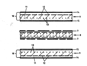
Between the two base substrates 28 there is provided one intermediate
substrate 33,~which is composed of a hard core layer 34 of a thickness
of~0,4~mm~màde~up of a matrix 35 of cured epoxy resin reinforced with
25~ ~- three ~UD~ filaments layers 36; and 37 extending in the 0 and 90
d~rections,~respectively. Here also the combined thickness of the two
outer UD layers~is equal to or virtually equal to the thickness of the
inner UD layer. ~he hard core layer 34 is provided on both sides with
a ~still~ plasti~cally deformable glue or adhesive layer 38 having a
thickness~ of 35 ~m. The adhesive layer 38 may be made up of the same
material as the glue layer 15 described hereinbefore. Next, the two
base~substrates 28 and the intermediate substrate 33 therebetween are
joined together under the effect of heat and pressure to form a
;~ laminate (the situation indicated in Fig. 14). In this process the
,
~ ~ .
::
~ ' .
WO 92/22192 2110 ~ PCI`/EP92/01133
hard core layer 34 of the intermediate substrate 33 is contacted or
virtually contacted on both sides with the opposing copper traees 29
of the base substrates 28, while the voids between these traces on
either side of the intermediate substrate are filled with the adhesive
S material 38. After the voids between the traces have been filled with
glue, said glue is cured, substantially completing a multilayer PWB
39. The PWB 39 has four layers of copper traces.
In Figs. 15 and 16 it is shown how in accordance with the principle
described for Figs. 13 and 14 it is also possible to manufacture a PWB
with six layers of copper traces, corresponding parts being
indicated with the same reference numerals. As is indicated in Fig.
15, use is made in this case of three base substrates 28. An
- intenmediate substrate 33 is sandwiched between each pair of base
substrates 28. In the manner described hereinbefore the combination
of three base substrates 28 and two intermediate substrates 33 shown
in Fig. 15 is next joined together under the effect of heat and
pressure into a laminate, which after the curing of the glue 38 forms
a virtually finished multilayer PWB 40 containing six layers of copper
traces. PWBs with a far greater number of layers of copper traces can
be manufactured in a similar manner.
The core of the intermediate substrate and of the base substrate may
be built up from a number of UD prepregs stacked in such a way that
their reinforcing filaments cross each other, it is also possible to
employ an alternative preparative process. Notably, the base substrate
and the intermediate substrate can be manufactured by a continuous
process, in which a laminate composed of the desired number of layers
of stretched reinforcing filaments not bound in the form of a fabric -
is laid on a conveyor belt, with the filaments of superposed layers
crossing each other. To the thus formed laminate of filament layers
liquid thermosetting resin is applied, after which the laminate
provided with resin is passed through a double belt press, in which,
under the effect of heat and pressure, the filament layers are
WO 92~22192 PCI`/EP92/01133
211~7~ `
' 14
impregnated with resin and the resin is cured. As it leaves the double
belt press the wholly or partially cured laminate can then be provided
on one or on both sides with the relatively thin, non-sticking gl'ue
layer mentioned hereinbefore, whereupon said intermediate substrate is
ready.
According to another conceivable process the cores of both the base
substrate and the intermediate substrate are manufactured from several
unidirectional laminates which preferably cross each other at an angle
of 90, are completely or virtually completely cured, and are bonded
together with the aid of an adhesi~e layer. Laminates based on
crossing UD laminates bonded together with an adhesive layer can be
manufactured in static, optionally multiopening presses, as well as in
autoclaves, double belt presses, and so-called vacuum bags.
.,
In an embodiment of the process according to the invention a
muitilayer PWB with four layers of copper traces was manufactured as
fol10ws: ~
- The starting material selected was a UD prepreg of Twaron~, an aramid
fibre~ex Akzoj an epoxy resin, in this case Epikote 828 ex Shell, and '-
a curi~ng;agent, in this case HY 917 ex Ciba Geigy. The fibre content
of~thè'?prepreg was 50~ of volume, the thickness 0,1 mm. The prepreg
was~cùt~;up~ nto ~12 square pieces measuring 610 x 610 mm. Two base
substrates;-'were~manufactured; in each manufacturing process, four of
these;-~pi~eces ~were; stacked between two copper foils, with the two
centre prepregs'~-disposed at an angle of 90 in relation to the top and
bottom UD'prepreg layers. The two stacks of materials thus made were
cured ~in an autoclave under a pressure of 8 Bar and at a temperature
; 30 ~ of 180C over' a period of three hours. The remaining four prepregs
; ~ were stacked~between two release films, with the two centre prepregs
; ~; rotated through an angle of 90 in relation to the top and bottom
layers of UD prepreg. This stack of material was also introduced into
an autoclave and then cured under the same conditions as the
: ~,
~ .
~ .
WO 92/221g2 PCI/EP92/01133
21105i7'~
aforementioned base substrates. Following the finishing of the three
thus formed laminates the desired patterns were etched into the copper
layers, while the release film was removed from the intermediate
substrate. The intermediate substrate was then coated with a glue also
based on Shell's Epikote 828 epoxy resin and filled with 30% fine
quartz powder. In a final step the three laminates were joined
together with the intermediate substrate at the centre, cf. also Fig.
13. This stack of laminates was placed in an autoclave and the epoxy-
glue layer cured under a pressure of 10 Bar and at a temperature of
180C over a period of 30 minutes. In this way a 4-layer multilayer as
- drawn in Fig. 14 was formed.
To said thermosetting matrix resin there may be added in a
conventional manner fillers such as fine quartz powder and, say, glass
powder such as boron silicate glass powder.
Although it is preferred to use a resin based on epoxy resin for the
base substrate matrix, it is also possible in principle to employ
other resins, such as cyanate resins, unsaturated polyester (UP)
resins, vinyl ester resins, acrylate resins, BT-epoxy restn,
- ~ bismaleimide resin (BMI), polyimide (PI), phenol resins, triazines,
polyurethanes, biscitraconic resin (~CI). Alternatively,-use may be
made of combinations of the aforementioned resins, and it is also
possible to blend said resins with certain appropriate thermoplastic
resins, such as PP0, PES, PSU, and, int. al., PEI.
A great many polymers are suitable to be used for the described glue
layer, more particularly thenmosetting resins, such as epoxy resin
(EP), polyurethane (PU), vinyl ester (VE), polyimide (PI),
bismaleimide (BMI), biscitraconic (BCI), cyanate esters, triazines,
acrylates, and blends thereof. Prior to application many additives can
~-~ be added to the glue, such as catalysts, inhibitors, thixotropic
agents, and especially fillers. These fillers are preferably selected
from the following group of materials: quartz powder, glass powder,
wo 92/221g2 P ~ /Eps2/ol133
2 1 1 0 6 7 9 16
ceramic powders, such as aluminium oxide powder. It is preferred that
the fillers to be used should have a low thermal coefficient of
expansion and a low dielectric constant. Favourable results can ~e
attained by using hollow spheres as filler, which spheres may be of
either a polymeric material or a ceramic material or glass.
For the aforementioned reinforcing filaments it is preferred to use
filament yarns, although it is also possible to use non-continuous
fibres. According to the invention the reinforcing yarns are
preferably selected from the following group of materials: glass, such
as E-glass, A-glass~ C-glass, D-glass, AR-glass, R-glass, S1-glass,
and S2-glass, and various ceramic materials, such as aluminium oxide
en silicon carbide. Furthermore, fibres based on polymers are
suitable, more particularly liquid crystalline polymers, such as
paraphenylene terephthalamide (PPDT), polybenzobisoxazole (PB0),
polybenzobisthiazole (PBT), and polybenzoimidazole (PBI), as well as
fibres based on polyethylene terephthalate (PETP) and polyphenylene
sulphide (PPS).
20 Within the frame~ork of the invention various changes may be made.
.
. .