Note: Descriptions are shown in the official language in which they were submitted.
WO 92/21949 PCT/DK92/00177
- 1 -
DETERMINATIOrf OF INDUCED CHANGE OF POLARIZATION STATE OF
LIGHT
1. BACKGROUNL) OF THE INVENTION
The Technical. Field
The present invention relates to a method of determining
induced chancre of polarization state of light in a polari-
zation elemer.~t, fiber optic sensor devices for determining
such induced change of polarization state of light,
particularly linear birefringence induced by an electric
voltage, an electric: field, and a mechanical force, and
circular birefringence induced by an electric current and
a magnetic field.
A magnetic field, an electric field, or a mechanical for-
ce, or a combination of these, can induce anisotropy in
the index of refraction of an optically transparent elec-
trooptic, magmetooptic and/or photoelastic material, re-
spectively, which can be detected by a change of polari-
zation state of light.
Linear birefringence can be induced by an electric field
in an electrooptic material by the so-called electrooptic
Pockels effects and Kerr effect which can be used in the
determinatior.~ of electric voltage and electric field;
circular birefringence can be induced by a magnetic field
in a magnetooptic material by the so-called magnetooptic
Faraday effect which can be used in the determination of
electric current and magnetic field; and
linear birefringence can be induced by a mechanical force
in a photoela.stic material by the so-called photoelastic
effect which can be used in the determination of me-
.._ _ _~...~._.~.. _ _ _..~_.._ _..Y_...,e _ _.. _.__.___ _..._,..
WO 92/21949 PCT/DK92/00177
- 2 -
~ll~irl~~
chanical force e.g. acceleration and pressure.
Generally, induced change of polarization state of light
in a polarization element is used in fiber optic polari-
metric optical sensors and the induced change can be
determined by:
a) transmitting unpolarized light from a light source at
the one end of an optical transmitter waveguide means
to polarizer means at the other end;
b) polarizing the unpolarized light by the polarizer
means;
c) transmitting the polarized light through a polarization
element;
d) analyzing the transmitted polarized light from the
polarization element by an analyzer means; and
e) transmitting the analyzed polarized light from the one
end of an optical receiver waveguide means to a light
detector at the other end;
wherein the unpolarized light is collimated by input coup-
ling means between the optical transmitter waveguide means
and the polarizer means, and the analyzed polarized light
is focused by output coupling means onto the optical
transmitter waveguide means, said coupling means consis-
ting of lenses or graded index rod lenses.
Specifically for a fiber optic magnetooptic current
sensor, it has been suggested that the transmission of the
polarized light through the polarization element is
provided by using at least one plane reflective optical
surface reflecting a collimated beam.
WO 92/21949 PGT/DK92/00177
21~.~'~~~
- 3 -
These optical arrangements have a number of disadvantages.
First of all, a collimated beam or slightly convergent
beam is used which requires auxiliary coupling lenses to
obtain an optimal Eight energy transmission from the op-
tical transmitter waveguide means to the optical receiver
waveguide means.
Secondly, thE; use of conventional lenses as coupling means
makes the sie of the arrangement inconveniently large be-
cause the lenses must be surrounded by air in order to
obtain a suil~ably large change of refractive index at the
optical surfaces.
Also, mechan:Lcal holders for the lenses are required which
complicates i~he mechanical construction.
Further, in i:he case of a voltage or electric field sensor
using conveni:ional lenses, the air present around the
lenses limits the electric field that can be applied to
the sensor before disruptive electric discharge occurs.
Graded index rod lenses may avoid the problem of air if
coupled direcaly on to the optical waveguide, such as an
optical fiber.. Such an arrangement can be made compact and
the optical interfaces can be filled with an electrically
insulating optical cement. However, in order for the
graded index rod lenses to collimate the beam from the
transmitter, a relative small core diameter (max. 200 um)
optical fiber is required which limits the amount of light
that can be 7.aunched into the optical fiber by the light
source, hereby limiting the signal-to-noise ratio and the
sensitivity of such a device, unless compensated for by a
more powerful. light source.
_._... ... .... . ~_.... ..v..........~...___..~...~...~. .. _._......___ .
_.....~_.. ......_d. ,.
CA 02110700 2000-06-29
- 4 -
Thus, cheap visible light emitting diodes e.g. LED's
emitting light in the range 500 - 700 nm cannot be used
because they cannot supply sufficient light through such
optical fibers havin<:~ that small core diameter. Instead
powerful and more expensive LED's emitting light in the
range 800 - 950 nm mu~~t be used. However, LED's and
polarizers working at these wavelengths as well as graded
index rod lenses are expensive.
Therefore, there is a need for a method of determining
induced change of polarization state of light in a
polarization element which can be implemented in a compact,
small and relatively cheap fiber optic sensor device.
Prior Art Disclosure
US Patent No. 3980949 discloses a magneto-optical measuring
transducer for measu.ri_ng both nominal and excessive high
currents, said transducer having a first magnetically
saturable part and a :second paramagnetical. part, the outer
surfaces of the first and second parts being provided with
reflective materials t:o provide multiple passages of
polarized light through the transducer. Nothing is indicated
or suggested about providing reflection by means of a
reflective imaging optical element and non-collimated light.
W.B. Spillman and D.H. McMahon, "Multimode Fiber Optic
Sensors Based on. the F?hotoelastic Effect", Proceedings of
Fiber Optics anc', Laser_ Sensors, Arlington, Virginia, April
5-7, 1983, SPIE, Vo1.412, Paper No. 412-17, p.110-114
disclose a multimode fiber optic sensor based on the
photoelastic effect :in which light from an input fiber is
collimated by a graded index rod lens, and the analyzed
light is separated into two components and injected into
WO 92/21949 PGT/DK92/00177
- 5 -
two output optical fibers via graded index rod lenses.
UK Patent Application Publication No. 2159944 discloses an
optical sensor, in particular an optical pressure sensor,
comprising an electrically switchable optical 90° rotator.
The sensor uses collimated~light and does not comprise a
reflective imaging optical element.
US Patent No. 4613811 discloses a fiber optic magnetooptic
current sensor for measuring current flowing through a
conductor comprising two components one of which has a
plane reflective surface for reflecting a polarized light
beam between the two components. Nothing is indicated or
suggested about reflecting the polarized light by means of
a reflective imaging optical element and non-collimated
light.
Hulshof et al., "Opt:ical Voltage Sensor: Application in
Electric Power Systems", SPIE Vol. 798, Fiber Optic Sen-
sors II, 1987, disclose a transmission type optical fiber
voltage sensor comprising a Pockels cell of bismuth-ger-
maniumoxide and conventional lenses or graded index rod
lenses as collimating or focusing coupling means.
EP Patent Application Publication No. 0284346 discloses an
optical interface coupled to a Faraday rotator device
disposed in surrounding proximity to an energy
transmission line in a magnetooptic current transducer
which interface comprises a collimator segment coupled to
a spacer lens element focusing a divergent beam of input
light from a fiber optic cable into a collimated beam
directed to the Faraday rotator device through a po-
larizing element by a parabolic surface.
US Patent No. 4841234 discloses a fiber optic voltage
detector comprising an optical probe having an electro-
_....,_..v..,___.._ .__..._._w ._..~.__.. __...,~ .._..__..a_W .
._.._~r_..~r~....__..,__w..._._...____-,_... ___..
CA 02110700 2000-06-29
- 6 -
optic material worked into a frusto-~~onical shape the tip of
which is coated with a reflecting mirror. The optical probe
comprises a collimator. providing collimated light which is
reflected by the reflecting mirror. Nothing is indicated or
suggested about providing reflection by means of a
reflective imaging optical element and non-collimated light.
US Patent No. 4948255 discloses a fiber optic optical
sensing device compr:i~~ing an element provided with two total
reflection surfaces causing the beam path to invert its
direction by 180°. ThE: device uses light collimated by e.g.
rod lenses and does not comprise a reflective imaging
optical element.
DE-A-2 017 863 d.isclo:>es a polarization element having
inclined input and ex~~_t faces .
2. DISCLOSURE OE' THE INVENTION
In a primary asP>ect, it is the object of the present
invention to prc~vide a method and a fiber optic sensor
device for determining induced change of polarization state
of light in a pc>larization element which method can be
carried out and be implemented in a compact, small, and
relatively chea~> device which is powered by a low power
output light source and easy to mount.
It is another object of the present invention to provide
such a method arid device which can withstand large
electrical fields without being subjected to disruptive
electric discharge.
Further, it is ~~till another object of the present invention
to provide such a method and device which has a good
temperature stability.
CA 02110700 2000-06-29
According to a broad aspect of the present invention there
is provided a method c>f determining :induced change of
polarization state oa light in a polarization element. The
method comprises tram>mitting unpolarized light from a light
source at the one end of an optical transmitter waveguide
means to polarizes means at the other end. The unpolarized
light is polarized by the polarizes means. The polarized
light is transmitted through the polarization element using
at least one reflective optical element. The transmitted
to polarized light is analyzed from the polarization element by
an analyzer means. The analyzed polarized light is
transmitted from the one end of an optical receiver
waveguide means to a 7_ight detector at the other end. The
optical transmitter waveguide means and the optical receiver
waveguide means are substantially parallel or coinciding.
The unpolarized light, while being polarized by the
polarizes means, and t:he polarized light, while being
analyzed by the analyzer means, or both, are non-collimated.
The light from the other end of the optical transmitter
waveguide means is reflected in the light path between the
polarizes means and the analyzer means by the at least one
reflective optical element so as to focus the reflected
polarized light onto the one end of the optical receiver
waveguide means. The light to be analyzed by the analyzer
means exits from the same side or parallel sides of the
polarization element as the polarized light polarized by the
polarizes means enters the polarization element. The
polarizes means is located directly adjacent to the other
end of the optical tr<~nsmitter waveguide means and the
analyzer means is located directly adjacent to the said one
end of the optical receiver waveguide means.
CA 02110700 2000-06-29
According to the invention the unpolarized light while being
polarized by the polariser means, the polarized light while
being analysed by the analyzer means, or both, are non-
collimated whereby auxiliary waveguide coupling means,
particularly collimat:i.ng and focusing coupling lenses, or
graded index rod lenses, are avoided.
Further, according to the invention :in combination with the
non-collimated light, the light from said other end of the
optical transmitter waveguide means :in the light path
between the polarizer_ means and the analyzer means is
reflected by at least one reflective optical element
focusing the reflected polarized light onto said one end of
the optical receiver waveguide means, whereby the
transmitter and receiver optical waveguide means can be
connected to the same side of the device.
In combination the twc> features provide the effect that
simultaneously components can be saved and focusing of the
reflected polarized light onto said one end of the optical
receiver waveguide means can be performed over a relatively
short length-to-width ratio whereby a compact device having
a relatively large proportion of active material compared to
the total volume can be obtained.
Also, because a reflective surface requires little volume
compared to len:ces, a relatively small device can be
obtained comparE~d to conventional lens devices because the
light path is used more efficiently by applying active
material in the space otherwise occupied by graded index rod
lenses or conventional lenses and air.
CA 02110700 2000-06-29
_ g
Further, because the optical transmitter and receiver
waveguide means can be connected to the same side of the
polarization element, the device can be made easy to mount,
particularly in appl.ic:ations where the quantity to be
measured only can be approached from the one side.
Also, by applying active material to the space otherwise
occupied by lenses and particularly by air, it can withstand
large electrical fields without being subject to disruptive
electric discharge.
Further, because e.g. graded index rod lenses can be
avoided, relatively cheap large core diameter optical
waveguide means having diameters in the range 200 - 1000 ~m
can be used. ThL:s, a better transmission efficiency of the
optical path through t:he apparatus from light source to
detector compared to sensors using conventional 50 - 100 Nm
optical fibres c:an be obtained. Further, an increased
signal-to-noise ratio and sensitivity is obtained compared
to conventional sensors, just as a comparable accuracy is
obtained at a lc>wer optical power level. Also, an increase
in sensitivity c;an be obtained by applying more reflective
imaging element:c which provide multiple transmissions
through the polarization element and increase the total
optical path in the polarization element.
Reflective Imag~_ng Optical Elements
According to the invention, the polarized light in the light
path between thE: pola_rizer means and the analyzer means is
reflected by at least one reflective optical element so that
the polarized light i;s transmitted one or more times through
the polarization element before being analyzed.
A simple embodiment involves only one focusing reflective
optical element,.
CA 02110700 2000-06-29
- 10 -
Therefore, in a preferred embodiment, the polarized light is
transmitted through the sensitive polarization element one
or more times, preferably once or twice, by one reflective
imaging optical element.
Generally, to obtain a greater sensitivity, the polarized
light can be transmitted through the polarization element a
multiple number of times by more reflective optical
elements, at least one of which is imaging.
l0
Specifically, a polarization element having a reflective
plane surface with apertures for the light input and output
and a reflective convex surface opposite to the plane
surface can provide a total of four transmissions of the
polarized light through the polarization element.
Therefore, in another preferred embodiment, the polarized
light is transmitted t=hrough the sensitive polarization
element one or more times, preferably one, two or four
times, by two reflective elements at least one of which is
imaging.
According to the invention, reflective imaging optical
elements can be provided by methods known in the art.
In a preferred embodiment, a reflective imaging optical
element consist: of a convex surface of the polarization
element coated with a reflective coating, the curvature of
which can be provided by methods known in the art of lens
manufacturing e"g. using ray tracing, provided the aperture
of the optical i~ransmitter waveguide means and the polarizer
means, the thickness .and index of refraction of the
polarizer means,. the length and index of refraction of
the polarization element, the thickness and index of
refraction of the analyzer means and the aperture of the
analyzer means and optical receiver waveguide means are
WO 92/21949 ~ ~ ~ ~ ~ ~ ~ PCT/DK92/00177
- 11 -
known.
Further, the reflective coating can be selected from re-
flective coatings known in the art including metallic
coatings such as A1, Ag, and Au, and dielectric coatings
such as quartz, ZnS, Ti02, Sb203.
In some case:a, particularly when expensive or fragile
polarization elements are applied, it may be preferred not
to provide the convex surface directly on the polarization
element, but on e.g. a planoconvex lens.
Therefore, in another preferred embodiment, the reflective
imaging optical element consists of a planoconvex lens
with a conve:~ surface coated with a reflective coating.
These lenses can be provided by methods known in the art
of lens manu:Eacturing including optical design by ray tra-
cing.
In other casE~s, it may be preferred to apply a reflective
diffractive optical element, particularly to avoid the
relatively costly process of manufacturing a convex sur-
face, which f~lements can be provided by methods known in
the art including methods for manufacturing holographic or
computer genE~rated diffractive optical elements (P.
Hariharan "Optical Holography", Cambridge University
Press, 1984; L. Solymar and D.J. Cooke "Volume Holography
and Volume Grating", Academic Press 1981; and R.R.A. Syms
"Practical Volume Holography", Claradon Press, Oxford
1990 ) .
Therefore, iii still another preferred embodiment, the re-
flective imaging optical element consists of a diffractive
optical elemE:nt .
_. .. _..e.~._.._ .. .._.. _._.._. _.v . ..., .._ _~...._ _ ..... ._.._
..x.~._. ._ ....... _.w..._..., ._.~.__ .. ._._..__. .._.__.. .. .._ ____ .
._.
CA 02110700 2000-06-29
- 12 -
Polarization ElE~ment
According to the invention, the polarization element
consists of
10
i) a sensitive polarization element comprising a suitable
polarization active material in which a magnetic field,
an electric: field, or a mechani~~al force can induce
anisotropy in the index of refraction, and
ii) optionally an auxiliary polarization element providing
phase retardation or polarization rotation of polarized
light.
Polarization active m<~terials, some of which have intrinsic
birefringence, ~~re known in the art and comprise:
a) electrooptic materials including crystals such as CdF,
GaAs, GaP, ~3-ZnS,. ZnSe, ZnTe, Bi9Ge3012, Bi12Ge02o,
Bi12Si02a, KHZP04, KDZP04, NH9HZPOa, NH9DZP04, LiNb03,
LitA03, KIC3, and quartz (Si02) , and electrooptic
polymer manufactured by poling of polymers such as
epoxy or polymetlzylmethacrylate containing an
electrooptic dye such as one or more azo dyes such as
Disperse Red 1 (4-(4-nitrophenylazo)-N-ethyl-N-2-
hydroxyeth~~lanil.ine), (by poling is meant a process in
which the polymer is brought to a phase transition from
a mobile si.ate to an immobile state under influence of
an electric. field, i.e. poling field, such that the
alignment to electrooptic dye due to the poling field
molecules :is preserved after removal of the field. The
poling pro~Jess is described in Allan Gottsche:
"Electroop-~ic and Magnetooptic Sensors for Advanced
Applications in Electric Powersystems", Electric Power
Engineerin~~ Department, Technical University of Denmark
Publication no. 9005 (1990));
WO 92/21949 PCT/DK92/00177
- 13 -
b) magnetooptic materials including glasses such as fused
silica, and diamagnetic glasses such as BK7, SF6, SF57,
SF58, SF5!3 ( Shott ) , FR-4, FR-5, FR-7 ( Hoya ) , and M-16
(Kigre), and crystals such as quartz (Si02.), EuF2,
Tb3A15012,. LiTbF4, ZnSe, CeF3, LaF3, Bi4Ge3012'
Bi12Ge020,. CdMnTe, Y3Fe5012 (YIG), TbxYx-1 (IG); and
c) photoelastic materials including glasses such as ZKN7,
FK5, BK7, SK14, SK16, F2, LaFN2, SF2, SF4, and SF5
(Schott).
All optical rnateria:Ls possess the magnetooptic Faraday
effect. However, the magnitude of the effect varies. Also,
some magnetooptic materials simultaneously show
electrooptic effect, e.g. materials such as Bi4Ge3012'
Bi12Ge020 and Bi12Si020.
The sensitive polarization element can consist of mate-
rials selectEad from materials having intrinsic birefrin-
gence, and the physical dimensions can be chosen so that
the intrinsic: birefringence provides for a ~/4 phase re-
tardation whereby an auxiliary polarization element can be
avoided.
The auxiliary polarization element can consist of a phase
retardation means preferable providing a phase retardation
of ~/4 comprising phase retardation materials known in the
art including dichroic retardation plates, mica retarda-
tion plates and quartz retardation plates, e.g. all such
plates sandwiched between glass plates. The auxiliary
polarization element is preferably used together with
electrooptic or photo-elastic materials having little or
no intrinsic birefringence.
As mentioned belaw, phase retardation means can be
provided for by reflective optical elements which direct
WO 92/21949 PCT/DK92/00177
- 14 -
the polalrlitJzed light through the polarization element
whereby an auxiliary polarization element is also avoided.
Temperature and Wavelength Stability Enhancement
Especially, the phase-retardation means may be incorpora-
ted so that a high tolerance against wavelength and tem-
perature instabilities are obtained.
Phase retardation based on reflection is rather insensiti-
ve to temperature changes as a change in physical dimen-
sions of a reflecting element, unlike birefringent phase
retardation elements, does not influence the amount of
phase retardation (H. Fabricius "Achromatic Prism Retarder
for Use in Polarimetric Sensors", Applied Optics, Vol. 30,
No. 4, 1991, pp. 426-429).
Therefore, according to the invention, phase-retardation
means include phase-retardation means based on reflection.
In a preferred embodiment, the reflective imaging optical
element consists of an optionally coated convex surface of
the polarization element reflecting by total internal
reflection.
In some cases, particularly where expensive or fragile
polarization elements are applied, it may be preferred not
to provide the convex surface directly on the polarization
element, but instead on an additional optical element.
Therefore, in another embodiment, the reflective imaging
optical element consists of an optionally coated convex
surface of an additional optical element reflecting by
total internal reflection.
WO 92/21949 PGT/DK92/00177
- 15 -
Because phasE: retardation only depends on total internal
reflection based on the indices of refraction of the ele-
ment itself and the surrounding air, it is pratically in-
sensitive to variations in temperature. The element con-
s sists of an optical material with a convex total internal
reflecting surface which, if chosen to be parabolic, is
able to collimate a divergent beam emitting from the focal
point of the parabolic surface, or vice versa, is able to
focus a collimated beam in the focal point. If not para-
bolic, the convex surface will still be able to provide
phase retardation, however, a collimated beam is not
obtained.
When reflected, optical rays fulfilling the angular requi-
rement of total internal reflection will obtain a phase
retardation which is a function of the index of refraction
of the element and the angle between the incident ray and
the reflected ray. Though each ray of the beam obtains a
somewhat different phase retardation, it is possible to
select the index of refraction of the element, provided
that the intE:nsity distribution of the optical beam is
known, so that a single reflection of the whole beam in
the surface will induce an effect, which when analyzed by
the analyzer and integrated on the detector can substitute
the effect of a ~/8 phase retardation element.
When an optical beam is reflected twice at a single sur-
face, or reflected at two different surfaces, the total
net effect on the optical power analyzed and integrated on
the detector can substitute for a ~/4 phase retardation
element.
Polarizer MeG~ns
The polarizes means comprises linear polarizers including
dichroic sheEa polarizers, glass polarizers (e. g. 8612
._._.._ _ _ ..... .... .. _.._.. ... ..._.........._ _ ... . ~.~ _...
~..._.._r...__..~__._.r....._._.__. _
CA 02110700 2000-06-29
- 16 -
PolarcorTM from (:orning) , polarizing beam splatters, and
calcite polarizers.
Analyzer Means
The analyzer means comprises means to discriminate between
the polarization state of light selected by the polarizer
means and the phase retardation means, if present, and the
polarization state of light leaving the polarization
element.
The analyzer means comprises the same type of linear
polarizers as mentioned for the polarizer means.
Optical Transmitter and Receiver Waveguide Means
Optical transmitter and receiver waveguide means comprises
optical fibers known in the art such as single and multimode
optical fibers, part:ic:ularly multimode fibers having large
cores are preferred.
Light Sources arid Detectors
Light sources comprise suitable light sources for coupling
to optical fibers including light emitting diodes (LED).
Particularly low cost LED's can be used in connection with
large core diameter optical fibers.
Light detectors comprise suitable light detectors for
coupling to optical fibers including PIN and avalanche
photodiodes and photot:ransistors which are able to detect
the light from the applied light source.
The optical power transmitted through the analyzer is
proportional to the optical power emitted by the light
source, but modL:lated by the measured quantity.
CA 02110700 2000-06-29
- 17 -
The modulated optical signal is detected by the light
detector end hereby converted to an electric current, which
by electronic amplif:ic:ation means is converted to an
electric voltage, the magnitude of which is proportional to
the optical power transmitted through the analyzer. The
component of the signal proportional to the measured
quantity can be extracted from noise signals and the
attenuation, due to :Loss in the optical system can be
compensated for by means of electronic signal conditioning
means, i.e. sigr..al processing electronics, known in the art
of fiber optical sens~_ng and polarimetric optical
measurement metr.ods. See e.g. Hulshof et al. ibid; Spillman
and McMahon ibid; and EP Patent Application Publication Nos.
0247842 and 0254396.
Sensor Devices
The invention relates to sensor devices particularly fiber
optic sensor devices for determining induced change of
polarization state o:f light in a polarization element.
According to a f-urther broad aspect of the present invention
there is provided a sensor device for determining induced
change of polarization state of light in a polarization
element. The device comprises an optical transmitter
waveguide means and an optical receiver waveguide means. A
polarizer means is provided for polarizing unpolarized light
emitted from the one end of the optical transmitter
waveguide means transrnitting unpolarized light from a light
source to the pc>larizer means. A polarization element
comprised of a ~>uitable polarization active material in
which an induced anisotropy in its index of refraction
changes the polarization state of the polarized light
polarized by the polar.izer means. A.t least one reflective
optical element is provided for reflecting the polarized
CA 02110700 2000-06-29
- 18 -
light transmitted through the polarization element. An
analyzer means is provided for analyzing the polarized light
reflected by the at Least one reflective optical element.
The analyzer means is positioned at one end of the optical
receiver waveguide means transmitting the analyzed light
from the analyzer means to detection means. The optical
transmitter waveguide means and the optical receiver
waveguide means are substantially parallel or coinciding.
The at least one reflective optical element is arranged to
focus light transmitted through the polarizes means from the
one end of the optical transmission waveguide means through
the analyzer means onto the one end of the optical receiver
waveguide means. The light to be analyzed by the analyzer
means exits from the same side or parallel sides of the
polarization element as the polarized light polarized by the
polarizes means enters the polarization element. The
polarizes means is located directly adjacent to one end of
the optical transmitter wavegui.de means and the analyzer
means is locatecdirectly adjacent to the one end of the
optical receiver waveguide means.
A simple embodiment involves only one reflective optical
element.
Therefore, in a preferred embodiment, the at least one
reflective optical element consists of one focusing
reflective optical element arranged to transmit the light
through the sensitive polarization element.
A greater sensitivity is obtained by transmitting the
polarized light through the polarization element a multiple
number of times by more reflective optical elements, at
least one of which is focusing.
Therefore, in another preferred embodiment, the at least one
reflective optical elc=ment consists of two reflective
optical element. at least one of which is focusing, arranged
CA 02110700 2000-06-29
- 19 -
to transmit the light through the sensitive polarization
element.
The at least one reflective optical element is selected from
a group consisting o:f,;
i) a convex surface of the polarization element
coated with a reflective coating;
ii) a planoconvex lens with a convex surface coated
l0 with ~~ ref.lective coating;
iii) a reflective diffractive optical element;
iv) an optionally coated convex surface of the
sensitive polarization element reflecting by
total internal reflection; and
v) an optionally coated convex surface of an
additional optical element reflecting by total
internal rep=lection.
In a preferred embodiment, the optical waveguide
transmission anc~ receiver means consist of one or more multi
mode optical fibers connected to one or more polarizes means
and analyzer me~~ns, respectively.
In a preferred embodiment, the polarization element consists
of a magnetooptic material; and circular birefringence is
induced in the polarization element by a magnetic field or
by an induced magnetic field from an electric current.
In another preferred f=mbodiment, the polarization element
consists of an electrooptic material and further comprises
phase retardation means; and linear birefringence is induced
in the polarization element by an electric field or by an
induced electric: field from an electric voltage.
In still another. embodiment, the polarization element
consists of a photoelastic material and further comprises
phase retardation means; and linear birefringence is
cMF, vuN:tr~~°,~au;~~~e~ 0;; ;,,~.., ~ ,"~ . w~ ~~~VL~V~~~~~i~~~
- 20 -
induced in th~a polarization ~lom~nt by macharacal forc~ or
an induced m~charical forco from acceleration or pressure.
Specificall;;, it should ba mentioned that simile se~sor
fiev ices, incor.~orating only a si ngle optical fiber cr a
s i ngle set of transreti t =er,% receiver opt i cai f i bar s , when
operated acca:-3ing tc s tarrc~ar d polar imo tr is p- sc rice, car.
only be used J:o perform measurements of dynamic signsis,
that is to sa;r impulse cr AC signals, because the D
componen t cf the trars~nitted orticzl signa=, as cbtaired
aftzr thm lig~a has passed th~ ana.yzer, ~! s useC :o y =he
cr i ver ~Lr~ui~. cf the sensor tc canpersata f o: dyr:a~r=c
lOSS in t~E C'ptiC~'.~ fi~E='S.
~5 Therefore, un_'.=_ss it is otherwise exFlicjtly stared, the
or ti ca:. sensor. devices described ar a used ~:, r:,aasur a c yna-
mic sig,:.a_5 , ~auc:~ ss A~ or imp=is=_ magna tic f isi3 , alac-
~t~.1~ rlel~, e~_~Cr.._T'lc ourrent, ~~ °:.vrl:: Vvl tY'3° Cr
C':ynafT.I~...
rc°Cha:aCa'_ s' c_~nals such as v-ibr anon, aC~elera t.ion c:r
dy:.amic prass~:re changes. Measurement of s;.at=c sig:.als
g -' ) c: ~ be per fo=-rued when usir_g more than a
~, i n~-s a..
s=ogle Set cT trar:amitter/receiver fibers ar.d poi=r_zers
Gnd analyzers.
~5
35
r.
r t;; v. ,
.~-r. v a
~~~ ~,;,t. .
CMp, ~l~tJ'hl~~N'1"it~'ti'~W!~,ii (iJ ~ i~{~~ 0°'J5 ~ ir~ui
~~~~~~3~~La~~w ?
W 1 A
21~~~00
- 21 -
a
CA 02110700 2000-06-29
- 22 -
Definition of E~:pressions
Within the present context the expression "fiber optic
sensor" is only intended to designate an optical sensor
device supplied with f=fiber optic waveguides for transmission
of light to and from t:he optical sensor device.
Therefore, the e~xpres;>ion "fiber optic sensor" does not
imply that~the fiber optical waveguides themselves are the
sensitive polarization elements, wherein a change of
polarization state of light occurs.
Within the present context the expression "linear
birefringence" cesignates the ability of an optical material
to split up an incident wave of polarized light into two
linearly polarized wave components, the polarization planes
of which are coinciding with characteristic directions of
the material. The wave components are being transmitted
with different ~~ropagation velocities, resulting in a phase
retardation of the transmitted wave generated by
recombination of the linearly polarized wave components
after passing of the material, thereby providing a change in
polarization state o.f the transmitted optical wave relative
to the incident wave.
Also, phase retardation can occur by letting a polarized
wave undergo a reflection at a non-zero angle, preferably as
total internal reflect-ion, or reflection by a reflective
coating.
Phase-retardation means consists either of one or more media
of anisotropy of refractive index, i.e. linear birefringent
media, or of reflecting surfaces or a combination of the
two. A phase retardation of ~/2 radian or ~,/4 wavelength
i.e. a ~,/4 wave~~late c:an convert linearly polarized light
CA 02110700 2000-06-29
- 23 -
into circularly polarized light which provides an optimal
offset for a working point for the detection of induced
linear birefringence, e.g. in electrooptic and photo-elastic
sensors.
Further, within the present context the expression "circular
birefringence" designates the phenomenon that a wave of
polarized light incident on a medium of anisotropy of
refractive index with respect to the direction of rotation
of circularly polarized light is separated into two counter
rotating circularly polarized polarization components with
different propagation velocities resulting in a polarization
rotation of the transmitted wave generated by recombination
of the circularly polarized polarization components after
passing of the material.
Circular birefringence causes the plane of polarization of
linearly polarized light to rotate.
A phase retardation of ~,/4 or ~/2 radians causes a change
from a linear to a circular polarization state.
Also, within the present context, when it is mentioned that
the unpolarized light polarized by the polarizer means and
the polarized light analyzed by the analyzer means; or both,
are non-collimated, t=he expression "noncol.limated"
designates that the :li.ght emitted by the optical waveguide
transmitter means propagate as a divergent beam through the
polarizer means and polarization element propagating
according to the physical laws of optical wave propagation
as defined by the nurnerical aperture and core diameter of
the optical transmitter waveguide means and the indices of
refraction of the polarizer means and polarization element,
and that the light collected and reflected by the at least
one reflective imaging optical element is reflected back
through the polarization element and analyzer means as a
convergent beam propagating according to the physical laws
CA 02110700 2000-06-29
- 24 -
of optical wave propagation as defined by the indices of
refraction of the polarization element and the analyzer
means and the aperture and focal length of the reflective
imaging optical element, and focused on to the one end of
the optical receiver waveguide means.
Further, within the present context it should implicitly be
understood that every time the expressions "polarization
element", "auxiliary polarization element", "phase-
retardation means", "polarizer means" and "analyzer means"
are mentioned, the characteristic optical axes of the
devices mentioned are aligned according to the art of
polarimetric measuremE:nt practice as described in optics
literature.
That is to say that for the measurement of induced linear
birefringence such as .Linear electrooptic effect or
photoelastic effect, t:he polarization axes of the polarizer
means and analyzer means and the so-called "fast" and "slow"
optical axes of the phase-retardation means and the
polarization element should all be aligned according to
polarimetric me~.surement practice. Accordingly for the
measurement of induced circular birefringence such as the
magnetooptic Faraday effect, the polarization axes of the
polarizer means and analyzer means and the "fast" and "slow"
axes of the auxiliary polarization element, if present, and
the "fast" and "'slow" axes of intrinsic birefringence in the
polarization element, if such intrinsic birefringence is
present, should all be aligned according to polarimetric
measurement practice .
Polarimetric me~isurement practice is described in the optics
literature, spec:ifica_L1y in:
1) Eugene Hecht: "Optics", 2n Edition, Addison-Wesley
Publishing Compan y Inc., World Student Series (1987);
CA 02110700 2000-06-29
- 25 -
2) A. Yariv and P. 5.'eh: "Optical waves in crystals",
Wiley-Interscienc:e Publication, (1984);
3) Allan Gottsche: "Electrooptic and Magnetooptic Sensors
for Advanced Applications in Electric Powersystems",
Electric Power Engineering Department, Technical
University of Denmark Publication no. 9005 (1990).
3. BRIEF DESCRIPTION OF THE DRAWINGS
Other objects anal advantages of the present invention will
become apparent from t:he detailed description and specific
examples only illustrating preferred embodiments with
reference to the drawings where
Fig. lA shows a preferred embodiment of a fiber optic
magnetooptic sensor device;
Fig. 1B shows a cross sectional view along the line Ib-Ib on
Fig. lA;
Fig. 1C shows another embodiment of the device in Fig. IA,
where the polarized :lught is passing the polarization
element four times;
Fig. 2 shows anc>ther embodiment of the device in Fig. 1;
Fig. 3 shows a ~>refe:rred embodiment of a fiber optic
magnetooptic sensor device comprising a di.ffractive optical
element as the reflect=ive imaging optical element:
Fig. 4 shows another embodiment of the device in Fig. 3
comprising one optical fiber transmitter and two optical
fiber receivers;
WO 92/21949 PCT/DK92/00177
- 26 -
Fig. 5A, 5H, 5C and 5D show preferred embodiments of an
electrooptic/photoelastic optical fiber sensor device;
Fig. 6A shows a preferred embodiment a magnetooptic opti-
cal fiber sensor device comprising one optical fiber si-
multaneously functioning as transmitter and receiver;
Fig. 6B shows a preferred embodiment of an electrooptic/-
photoelastic sensor device comprising one optical fiber
simultaneously functioning as transmitter and receiver;
Fig. 7A shows a preferred embodiments of an electrooptic/-
photoelastic sensor device comprising a combination of an
additional optical element including a reflective imaging
optical surface and a plane mirror substituting a ~./4
optical element;
Fig. 7B shows another embodiment of the device in Fig. 7A
where the sensitive polarization element is positioned
between the reflective imaging optical element and the
plane mirror;
Fig. 7C shows another embodiment of the device in Fig. 7A,
where the reflective imaging optical surface is a convex
surface of the sensitive polarization element;
Fig. 7D shows another embodiment of the device in Fig. 7A,
where the additional optical element comprising a
reflective imaging optical surface is constituted by a
plano-convex lens mounted on a plane surface of the sen-
sitive polarization element;
Fig. 7E shows a cross sectional view along the lines VIIe-
VIIe on Fig. 7A and Fig. 7D for preferred embodiments
using one or two optical fibers, respectively;
WO 92/21949 PCT/DK92/00177
~z~~~oo
- 27 -
Fig. 7F showsc a cross sectional view along the lines VIIf-
VIIf in Fig. 7B and Fig. 7C for preferred embodiments
using one or two optical fibers, respectively;
Fig. 7G shows. another embodiment of an electrooptic/photo-
elastic sensor device comprising a combination of a
polarization element having a reflective imaging optical
surface and a.n additional optical element including a
plane total internal. reflective surface having phase
retarding properties for the substitution of a ~/4 optical
element;
Fig. 7H shows. a cross sectionsl view along the lines VIIh
VIIh in Fig. 7G for preferred embodiments using one or two
optical fibers, respectively;
Fig. 8A shows. another embodiment of the device in Fig. 7A
comprising two phase retardation elements;
Fig. 8B shows another embodiment of the device in Fig. 7B
comprising two phasE: retardation elements;
Fig. 9 shows an application of a magnetooptic fiber optic
sensor device according to the invention placed in a
magnetic field integrating core;
Fig. l0A shows an application of an electrooptic sensor
device according to the invention placed between the elec-
trodes of a voltage sensor;
Fig. lOB shows an application of the temperature and
wavelength stability enhanced electrooptic sensor device
shown in Fig. 7C according to the invention placed between
the electrodes of a voltage sensor;
WO 92/21949 PCT/DK92/00177
- 28 -
?1~(~'~~~~
Fig. lOC shows an application of the temperature and
wavelength stability enhanced electrooptic sensor device
shown in Fig. 7D according to the invention placed between
the electrodes of a voltage sensor; .
Fig. 11 shows an application of an electrooptic sensor
device along with a magnetooptic sensor device including a
magnetic field integrating core, both of which devices
according to the invention are placed inside an electri-
cally grounded bushing surrounding a single conductor of
an electrical cable.
Fig. 12 shows an application of a photoelastic sensor
device according to the invention placed between a float-
ing mass and a support for measuring acceleration; and
Fig. 13 shows an application of a photoelastic sensor
device according to the invention which is connected via a
rod to a membrane for measuring pressure.
4. DETAILED DESCRIPTION
According to the invention, the method and apparatus for
determining induced change of polarization state of light
in a polarization element can be used both for linearly
and circularly induced birefringence in the polarization
element, depending on whether the polarization active ma-
terial is magnetooptic, electrooptic, or photoelastic. The
only difference being the requirement of phase retardation
means in case of linearly induced birefringence in
electrooptic and photoelastic materials.
Thus, the detailed description of preferred embodiments
should be taken to illustrate both types of birefringence,
even if not explicitely stated.
WO 92/21949 PCT/DK92/00177
If not otherwise explicitly stated, the optical axes of
all optical elements have been aligned according to
polarimetric measurement practice as mentioned earlier.
Magnetooptic Optical Fiber Sensor Devices
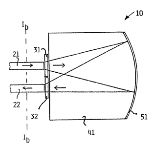
Fig. 1 shows a preferred embodiment of a magnetooptic
fiber optic sensor device 10.
Unpolarized light is transmitted from a light source (not
shown) at the one end of an optical fiber transmitter 21,
e.g. 600 um core multimode plastic-clad-silica fiber
TECSTM, Technology-Enhanced Clad Silica, FT-600-LMT (3M),
to a polarizer means 31 consisting of a linear polarizer,
e.g. a 8612 PolarcorTM glass polarizer from Corning, at the
other end.
The unpolarized diverging light from the optical fiber 21
is polarized linearly by the polarizer 31, and transmitted
through a polarization element 41 consisting of a
circularly birefringent magnetooptic material causing
polarization rotation when subjected to magnetic fields,
e.g. the glass SF6 from Schott.
The linearly polarized but polarization rotated light is
collected and reflected back through the polarization
element 41 by a reflective optical surface 51 obtaining
further polarization rotation. The reflective imaging op-
tical surface 51 is a convex surface of the polarization
element 41 which .is coated with a reflective coating of
aluminum.
The reflected light is focused through an analyzer means
32 consisting of a linear polarizer, e.g. a 8612 Polarcor~
glass polariz~er from Corning, transmitting the linearly
polarised light of a selected polarization on to the one
CA 02110700 2000-06-29
- 30 -
end of an optical fibE:r receiver 22, e.g. 600 ~m core
multimode plastic-clad-silica fiber TECSTM, Technology-
Enhanced Clad Silica, FT-600-LMT (3M), transmitting the
analyzed light to a :L~_ght detector (not shown) at the other
end of the fiber.
Thus, applying a. magnetic field, a change of polarization
state of light in the polarization element 41 can be
determined from the change of light intensity detected by
the light detector.
Because of the ~.ymmetry of rotation of the polarization
element 41, the convex surface 51, and the planoconvex lens
52, if present (see Fig. 2), more sets of polarizers and
analyzers and transm:it:ter and receiver fibers (see Fig. 1B)
can be positioned around the axis of symmetry e.g. for a
more thorough polarization analysis for the measurement of
static magnetic field or DC current.
Fig. 1B shows a cross sectional view along the line Ib-Ib on
Fig. lA indicating sets of polarizers and analyzers 31,32
and 31A, 32A, and the optical fiber transmitter/receivers
21, 22 and 21A, 22A, respectively.
Fig. 1C shows another embodiment of the device in Fig. lA
comprising a second reflective optical element, which
optionally may ~~e imaging, but is shown here as a plane
surface 54 coated with a reflective coating, except in the
two apertures, where t=he light from the optical transmitter
fiber 21 is allowed to be transmitted from the polarizer 31
into the polarization element 41, and the reflected light is
transmitted from the polarization element 41 through the
analyzer 32 and into t=he receiver fiber 22. The light from
the transmitter fiber 21 is collected by t:he reflective
optical imaging surface 51 and reflected back through the
polarization element 41, here shown specifically in a
CA 02110700 2000-06-29
- 31 -
collimated form, reflected forward again, still in a
collimated form, by the reflective optical surface 54, and
finally collected once again by the reflective optical
imaging surface 51 and reflected back through the
polarization element 41 again, while being focused on the
receiver optical fiber 22. In this way, the polarized light
is transmitted through the polarization element 41 a total
of four times, hereby yielding a higher sensitivity of the
sensor device.
It should be noted that the reflections within the
polarization element are not restricted to light in a
collimated form. Further, it should be noted that the
transmission of the polarized light four times through the
polarization element c:an be accomplished with either one of
the reflective optical_ elements being imaging and the other
being non-imaging or with both of the reflective optical
elements being imagine. Consequently, it is also possible to
let both of the reflecaive optical surfaces 51, 54 be convex
imaging surfaces, or 7_et the reflective optical surface 51
be a plane reflective surface and the reflective optical
surface 54 be an imaging convex surface. By designing the
two reflective optical elements correctly, it is
theoretically possible to select the number of double-passes
of the polarizes. light: through the polarization element as
any positive integer.
Fig. 2 shows another embodiment of the device in Fig. 1
comprising a planoconvex lens, 52 having a convex surface
coated with a reflective coating of aluminum and coupled to
the polarization. element 41. Optical cement, optical epoxy,
or other materials may optionally be applied between the
lens and the polarization element.
Fig. 3 shows another preferred embodiment of a magnetooptic
optical fiber sensor device comprising a diffractive
WO 92/21949 PCT/DK92/00177
~,~~'~~~~
- 32 -
optical element 61 as the reflective imaging optical
element.
Fig. 4 shows another embodiment of the device in Fig. 3
comprising one optical fiber transmitter 21 and two opti-
cal fiber receivers 22A, 22B. The number of optical fiber
transmitters and receivers can be increased. Thus, one
transmitter and four receivers can be used for the mea-
surement of static signals, e.g. do current.
Electrooptic/Photoelastic Optical Fiber Sensor Devices
Fig. 5A show preferred embodiments of an electrooptic/-
photoelastic optical fiber sensor device 11.
Unpolarized light is transmitted from a light source (not
shown) at the one end of an optical fiber transmitter 21,
e.g. a 600 um core multimode plastic-clad-silica fiber
TECS~, Technology-Enhanced Clad Silica, FT-600-LMT (3M),
to a polarizer means 31 consisting of a linear polarizer,
e.g. a 8612 PolarcorTM glass polarizer from Corning, at the
other end.
The unpolarized diverging light from the optical fiber 21
is polarized linearly by the polarizer 31, and retarded by
an auxiliary polarization element 41B consisting of a thin
disc of linear birefringent material, e.g. a ~/4 quartz
retardation plate. The retarded polarized light is then
transmitted through a sensitive polarization element 41A
and is subjected to induced phase retardation in the
element. The element consists of a linear birefringent
electrooptic polymer manufactured by poling of epoxy
containing a sufficient concentration of the electrooptic
azo dye Disperse Red 1 with the systematic name 4-(4-
nitrophenylazo)-N-ethyl-N-2-hydroxyethylaniline. In case
of a photoelastic sensor device, the polarization element
CA 02110700 2000-06-29
- 33 -
41A consists of a linear birefringent photoelastic material,
e.g. ZKN7 glass from :3chott.
The circularly polarized light is collected and reflected
back through the sensitive, polarization element 41A by a
reflective optical surface 51 and hereby being subjected to
further phase retardat:ion. The reflective imaging optical
surface 51 is a convex surface of the sensitive polarization
element 41A which is coated with a reflective coating of
aluminum.
The reflected light i:> focused through the analyzer means 32
consisting of a linear polarizer, e.g. a 8612 PolarcorTM
polarizer from Corning, transmitting a linearly polarised
component of selected polarization on to the one end of an
optical fiber receiver 22, e.g. a 600 ~m core multimode
plastic-clad-silica fiber TECSTM, Technology-Enhanced Clad
Silica, FT-600-LMT (3M), transmitting the analyzed light to
a light detector (not shown) at the other end of the fiber.
Thus, applying an elects ric field or mechanical force, a
change of polarization state of light in the sensitive
polarization element ~LlA can be determined by the change of
light intensity detected by the light detector.
In Fig. 5B, the auxiliary polarization element 41B is
positioned between the analyzer means 32 and the
polarization element ~!:l.
In Fig. 5C, the auxiliary polarization element 41B is
integral with the sent>itive polarization element 41A.
In Fig. 5D, the auxiliary polarization element 41B includes
the reflective imagine optical surfa~~e 51.
CA 02110700 2000-06-29
- 34 -
It should be noted that the embodiments of the reflective
imaging optical element in Figs. 2,3 and 4 consisting of the
planoconvex lens. 52 and the diffractive optical element 61
can also be implemented for this electrooptic/photoelastic
sensor device. Likewise more sets of polarizers and
analyzers, and auxiliary polarization elements and
transmitter/receiver f=fibers can be applied parallel to what
is shown in Fig. 1B and Fig. 4.
Magnetooptic/ Electrooptic/ Photoelastic Fiber optic sensor
Devices Using Or.~e Opt~~ cal Fiber
Fig. 6A shows a preferred embodiment of a magnetooptic fiber
optic sensor device comprising one optical fiber
simultaneously functioning as transmitter and receiver.
Unpolarized light is transmitted from a light source (not
shown) to a bean: split:ter or fiber splatter (not shown) and
a collimator lens (not. shown) at the one end of an optical
z0 fiber transmitter/receiver 23, e.g. a 600 ~.m core multimode
plastic-clad-silica fiber TECSTM, Technology-Enhanced Clad
Silica, FT-600-ZMT (3M), to a polarizes means 31 consisting
of a linear polarizes, e.g. a 8612 PolarcorTM glass
polarizes from Corning, at the other end.
ZS
The unpolarized divergent light from the optical fiber 23 is
polarized linearly by the polarizer/analyzer means 31, and
phase retarded by an auxiliary polarization element 41B
consisting of a thin a./4 disc of linear birefringent
30 material, e.g. a ~,/4 quartz retardation plate, and
transmitted through a sensitive polarization element 41A.
The polarization rotated light is collected and reflected
back through the sensitive polarization element 41A by a
35 reflective optical surface 51 hereby obtaining further
CA 02110700 2000-06-29
- 35 -
rotation of the polarization. The reflective imaging
optical element consists of a convex surface of the
sensitive polarization element 41A which is coated with a
reflective coating of aluminum.
The reflected light i:> focused and transmitted through the
~,/4 retarder means providing a total phase retardation of
~,/2 resulting in a rogation of the plane of polarization of
~/4 radians, and through the polarize=r/analyzer means 31
consisting of a linear polarizer, e.g. a 8612 PolarcorTM
glass polarizer from Corning, transmitting linearly
polarised light of a :>elected polarization on to the optical
fiber transmitter/recE:iver 23, transmitting the analyzed
light via a collimator. lens (not shown) and a beam splitter
or fiber splitter (not. shown) to a light detector (not
shown) at the other end of the fiber.
Thus, by applying a rnagnetic field, a change of polarization
state of light in the sensitive polarization element 41A can
be determined by the change of light intensity detected by
the light detector.
Fig. 6B shows a preferred embodiment of an
electrooptic/photoela~;tic sensor device comprising one
optical fiber simultaneously functioning as transmitter and
receiver.
The device is similar to the device shown in Fig. 6A except
for the sensitive polarization element 41A being an
electrooptic/photoela~;tic material and the auxiliary
polarization element 91B being a ~,/8 plate consisting of-a
thin disc of linear birefringent material which provides the
necessary 7~/4 phase retardation when passed twice by the
optical beam.
:35
CA 02110700 2000-06-29
- 36 -
Temperature and Wavelf=ngth Stability Enhanced Polarization
Sensor Devices
Fig. 7A shows a preferred embodiment of an electrooptic
photoelastic sensor device comprising an additional optical
element 53 including a total internal reflective imaging
optical surface 51A providing a temperature and wavelength
stable phase retardation and including a reflective optical
element optionally imaging, here shown as a plane reflective
surface 54.
In Fig. 7A the optica7_ path is similar to the one in Fig. 5A
and 5B and 5C ar.d Fig. 6A and 6B except for the single
reflective imaging optical surface 51 being replaced by a
parabolic total internal reflective imaging optical surface
51A on an additional optical element 53 providing a phase-
retardation yielding a net effect on the reflected optical
beam substituting for a ~,/8 phase retardation. Consequently,
two reflections of the optical beam in the surface 51A
substitutes for a ~,/4 phase retardation, whereby the
birefringent auxiliary polarization element 41B can be
avoided.
The embodiments using two optical fibers are illustrated in
Fig. 7E (b) and 7F (b) .
In Fig. 7E (b) there i.s shown cross sectional views along
the lines VIIe-VIIe in Fig. 7A and 7D.
In Fig. 7F (b) there i.s shown cross sectional views along
the lines VIIf-VIIf in Fig. 7B and 7C.
The embodiments using one optical fiber are illustrated on
Fig. 7E (a) and Fig. 7D (a).
CA 02110700 2000-06-29
- 37 -
In the embodiments shown in Figs. 7A-7F, the unpolarized
diverging light from t:he transmitter optical fiber is
polarized linearly by the polarizer and transmitted through
the sensitive polarization element 41A, entering the
additional optical element 53 where it is reflected and
collimated by the total internal reflective imaging optical
surface 51A and directed on to a plane reflective surface 54
reflecting the light back through its original path. The
surface 51A may be optionally coated with a coating of
l0 selected refractive index providing optimal amount of phase
retardation. As the polarized light is phase retarded twice
by the internal reflection, a total effect on the
transmitted optical beam is obtained. This substitutes for
the effect of a ~,/4 phase retardation when the beam is
analyzed by the analyzer and the optical power is integrated
on the detector. To ~:~et an effect as close as possible to a
7~/4 phase retardation, glasses such as BaK4 or PSK3 (Schott)
can be used for the manufacture of the optical element
comprising the total .i_nternal reflective imaging optical
surface 51A. (H. Fabricius "Achromatic Prism Retarder for
Use in Polarimetric Sensors", Applied Optics, Vol. 30, No.
4, 1991, p. 426-429).
It should be noted that the phase retarding parabolic
surface element providing the effect substituting for a ~,/4
phase retarder is not a true ~,/4 plate as it provides
different retardation angles for parts of the beam emitted
at different solid angles. The net effect first appears
after the analyzer when the light is integrated on the
detector.
Fig. 7C shows an embodiment of the device in Fig. 7A, where
the additional optical_ element 53 is avoided by forming the
total internal r_eflect:ive imaging optical surface 51A in the
sensitive polarization element 41A itself.
CA 02110700 2000-06-29
- 38 -
Fig. 7D shows an embodiment of the device in Fig. 7A, where
the additional cptica7_ element 53 is constituted by a plano-
convex lens 53, mounted on a plane surface of the sensitive
polarization element ~11A with the convex surface of the lens
constituting the total internal reflective imaging optical
surface 51A. Optical cement, optical epoxy, or other
materials may optiona7_ly be applied between the lens and the
polarization element.
Fig. 7G shows another embodiment of an electrooptic/
photoelastic sensor device comprising a combination of a
polarization element ~!1 having a reflective imaging optical
surface 51 and an additional optical element 53 including a
plane total internal reflective surface 51A having phase
retarding properties f:or the substitution of a ~,/4 optical
element.
It should be noted that for this embodiment, the variation
in phase retardation obtained for individual optical rays
emitted at different ~>olid angles from the optical fiber is
greater than for the embodiments using an imaging total
infernal reflective surface phase retardation means.
Therefore the present embodiment provides a poorer
substitution for a ~,/9 or ~,/8 phase-retarder. However, the
simple geometry using a plane total internal reflective
surface simplifies manufacturing of the device.
The optical paths which can be used :in Fig. 7G are shown in
Fig. 7H. The embodiments using two fibers are illustrated in
Fig. 7H (b) showing a cross sectional view along the line
VIIh-VIIh. The embodiments using one optical fiber are
illustrated in Fig. 7H (a).
CA 02110700 2000-06-29
- 39 -
Fig. 8A shows another embodiment of the device in Fig. 7A
comprising two ~>hase retardation elements.
Unpolarized light provided by the optical fiber transmitter
21, e.g. a 600 N,m corE: multimode plastic-clad-silica fiber
TECSTM, Technology-Enhanced Clad Silica, FT-600-LMT (3M), is
polarized by the polarizer 31, e.g. a 8612 PolarcorT"" glass
polarizer from Corning, transmitted through the sensitive
polarization element ~llA to a parabolic phase retarding
surface 51A of an additional optical element 53 collimating
and phase retarc.ing the polarized light onto another
parabolic phase retarding surface 51B focusing the polarized
light through the sen:~itive polarization element 41A, an
analyzer 32, e.g. a ;3E>12 PolarcorTM glass polarizer from
Corning, and onto an optical fiber receiver 22.
Fig. 8B shows another embodiment of the device in Fig. 7B
where the sensitive polarization element 41A is placed
between two additional. optical elements 53A and 53B.
5. EXAMPLES
Applications
EXAMPLE 1
"Magnetooptic Fiber 0~>tical Sensing"
Fig. 9 shows an application of a magnetooptic fiber optic
sensor device accordir.~g to the invention positioned in a
magnetic field concentrator core 91 around an AC current
carrying conductor 92.
The concentrator core served the purpose of concentrating
:35 the magnetic field of the current in the conductor in the
WO 92/21949 PCT/DK92/00177
- 40 -
gap of the core, whereby a measurement of the magnetic
field in the total volume of the gap of the concentrator
core has proved to be a good approximation to an integra-
tion of the magnetic field in air along an arbitrary path
incirculating the conductor,, which according to Ampeeres
law yields the current in the conductor. Therefore, when
as according to the invention, the gap of the concentrator
core is almost fully occupied with the magnetooptic
material, the output from the magnetooptic sensor measu-
ring the magnetic field in the gap, yields, when correctly
calibrated by electronic means, a very reliable measu-
rement of the current which is only very little sensitive
to ambient magnetic fields and field perturbations and
only little sensitive to the position of the conductor
inside the aperture of the concentrator core.
If there are no ambient magnetic fields and no magnetic
field perturbing objects present, the magnetic field
strength around the conductor is directly proportional to
the current flowing in the conductor and inversely pro-
portional to the square of the distance to the conductor.
Therefore, assuming an unperturbed magnetic field and
measuring a small portion of the field by a magnetooptic
sensor a result is obtained, which, when properly cali-
brated for the distance to the conductor and the sensor
characteristics by electronic means, will be a correct
measurement of the current. Therefore, for some appli-
cations, the magnetic integrator core can be avoided and
the magnetic field sensor directly applied.
Because of the compactness of the magnetooptic sensor it
can be used to measure current even where only very little
space is available. For example an application of the
magnetooptic sensor is to measure current in a 10-20 kV
electric power distribution cable, when the sensor with or
without integrator core is placed inside a bushing
CA 02110700 2000-06-29
- 41 -
terminating a single conductor of the cable. (Fig. 11).
If the application is not critical and only low accuracy is
needed, the integrator_ core can be avoided.
EXAMPLE 2
"Electrooptic Fiber Optical Sensing"
l0 Fig. l0A shows an app7_ication of an electrooptic sensor
device according to the invention fixed between the
electrodes 94,95 of a voltage sensor cast in an insulating
material.
When sensor characteristics are properly calibrated for by
electronic means, the output from an electrooptic sensor
placed in a homogeneous AC electric field can provide a
measure of the field ~>trength of the field. When the
electrooptic sensor was placed in a fixed geometry between a
set of two electrodes, the output signal could be calibrated
to directly represent the voltage across the electrodes.
When the electrcoptic material appli~=d was a material with
high dielectric strength such as the electrooptic polymer
described in the Ph.D.-thesis by Allan Gottsche:
"Magnetooptic and Elec:trooptic Sensors for Advanced
Applications in Electric Power Systems", Publication No.
9005, (1990) Electric Power Engineering Department,
Technical University of Denmark, it was possible to have
high voltage directly across electrodes mounted on the
electrooptic material. Because, the voltage sensor was cast
in an electrically in~:ulating materi<~l, it could be safely
operated at voltages, at which a voltage sensor equipped
with conventional lenses would suffer from electric
discharge in the air pockets surrounding the lenses.
WO 92/21949 PCT/DK92/00177
- 42 -
When electrooptic crystals were used as the electrooptic
material, only relatively low voltage could be applied
directly across the crystal. However, as the crystal is
sensitive to electric fields, the electrooptic sensor can
be cast into a block of insulating material, the dimension
of which is considerably larger than the dimension of the
electrooptic crystal. When the block of insulating
material is equipped with electrodes and a voltage is
applied, the voltage across the crystal is only a fraction
of the voltage across the electrodes, as determined by the
ratio of the thickness of the crystal to the distance
between the electrodes and by the dielectric constants of
the crystal and the insulating material.
When implemented as described above, the voltage sensor
was used to measure voltage even where only very little
space was available. For an example an application of the
voltage sensor was to measure voltage on a 10-20 kV
electric power distribution cable, when the sensor was
placed between the conductor and an electrically grounded
outer shield of a bushing terminating a single conductor
of the cable.
Fig. lOB shows an application of an electrooptic sensor
device according to the invention fixed between the
electrodes 94, 95 of a voltage sensor cast in an electri-
cal insulating material.
The device was similar to the one shown in Fig. 10A,
except that phase retardation was provided for by the
total internal reflective imaging optical surface of the
polarization element as shown more detailed in Fig. 7C.
An air space 111 between the top electrode 94 and the
polarization element 41 provided the necessary shift in
index of refraction to provide for total internal
WO 92/21949 PCT/DK92/00177
- 43 -
reflection.
The device exhibited the same characteristics as described
for Fig. 10A, except for being less temperatu=re sensitive.
Fig. lOC shows an application of an electrooptic sensor
device according to the invention fixed between electrodes
94, 95 of a voltage sensor cast in an electrical
insulating material. The device was similar to the one
shown in Fig. lOB, except that the total internal reflec-
tive surface was pravided for by the plane surface of the
plano-convex lens (53) made of BaK4 glass (Schott) mounted
on a plane surface of the polarization element. The device
exhibited the same characteristics as described for Fig.
lOB, including good tolerance against temperture shifts.
Fig. 11 showsc an application of an electrooptic sensor
device combined with a magnetooptic sensor device
including a ~riagnetic field integrating core, both of which
devices according to the invention are placed inside a
cable bushing (93) consisting of an electrically grounded
metal tube surrounding a single phase conductor (92) of an
electrical 10 kV distribution cable. The magnetooptic
sensor device: (10) was mounted with the magnetic field
integrating core (91.) surrounding the single phase
conductor (92) and its primary electrical insulation 110.
The electrooptic sensor device 11 was mounted between the
insulated phase conductor and the surrounding electrically
grounded bushing. The electrooptic sensor device was not
equipped with. electrodes, but simply exposed to the
electrical field between the phase conductor and the
surrounding bushing. The optical fibers of the sensing
devices were led through holes machined in the bushing for
that purpose (not shown). The test demonstrated that it
was possible to mount and operate the electrooptic and
magnetooptic sensor devices within the confined space
WO 92/21949 PCT/DK92/00177
- 44 -
.1 P;
c°d .~ ~ U ~ i,~ .~
available between the phase conductor and the outer
shielding of the cable bushing of a 10 kV distribution
cable.
EXAMPLE 3
"Photoelastic Fiber Optical Sensing"
Fig. 12 shows an application of a photoelastic sensor
device as an accelerometer, according to the invention
positioned between a floating mass 97 and a support 98.
When the support was accelerated, mechanical tension would
cause induced linear birefringence to build up in the
material through photoelastic effect because of the iner-
tia of the mass as stated by Newtons laws. When applied as
described above the photoelastic sensor could be used as
an accelerometer.
A typical example of an application is to monitor vibra-
tions on machine parts hereby determining the present
condition and extrapolated lifetimes of the machine parts.
Fig. 13 shows an application of a photoelastic sensor de-
vice according to the invention which is connected via a
rod (99) to a membrane (100) for measuring dynamic pres-
sure changes.
Differential presssure applied across the membrane
resulted in mechanical forces, which via the rod provided
mechanical tension in the photoelastic material causing
induced linear birefringence to build up through the pho-
toeleastic effect. When applied in this way, the photoela-
stic sensor was used to measure dynamic pressure changes.
An application would be to measure pressure fluctuations
WO 92/21949 PCT/DK92/00177
- 45 -
in circulatir.~g fluid due to pump strokes. A typical exam-
ple of this application would be the measurement of dif-
ferential preasure between systolic and diastolic blood
pressure in the human body.
10
20
30