Note: Descriptions are shown in the official language in which they were submitted.
W~ ~2/22961 PCr/US92/04892
2 .L .~
REVERSIBLE ANAL06 TO DIGITAL CONVERTER (ADC-DAC) WITH ANAL06 AND DIGITAL
SIGNAL PROCESSIN6 AND ENCODING FUNCTIONS
Field o~ tlae T~r1ve~iol~
This invention relates generally to arlalog to
digital c~n~erter c:ircuitry and, in particular, to
embodiments o~ ~;implif ied analog to digital
conv~rter cells and ~o analog to di~ital cor.verters
constructed ther~rom.
An analos~ to d~ gital ~:onYerter gADC) converts an
analog ~ignal into a ~iscr~te ~inary codQ ~;uitable
~or digital processi~g. Th~re are 8~ eral ~actors
that det@r~ine wheth~r or not a particular ADC is
suit~d t~ a partiGular applic:a~ion, including
aomplex~y, C05t, c:onversion ti~e, r~solution,
ac~rac:~r an~l per:eormance o~rer temp ra~ure.
~owQv~rl : the Al:~C~s c urrently available hav~
. .
nu~rous def ici enci~s in o~e or ~ore of t:hose
areas r , ,..: ,,~, ,, .:.,. ,., , ~
~, , s .,~ y J~ ,? j ~:
U.S. ~?ag~nt 3"96 ,4~; teaches an ~DC th2c utilizes
a plurality o~ ~nalog ~ c,o~paral:ors, whsrairl ~ac:h
comp~rator receiYing an analosr~ inpa~ signal and a
separa~e unis~u@ r~ference signal. q~he total analog
t:o: d~gital comr~r~;ion I:ime is ~T, wher~ n i8 ~lf~
nu~er of co~parator s. ag~s a~d T is the respon~;e
tlm~ o~ he compara1~or. ~. . U . S . Paten~ 4, 59g ~ 602
t~ache~; a s~rial type ADC: utilizirlg folding circuit
cëlls. The first ceIl rec:eives a r~fer~nc:e
voltage. ~:ach cell's output sigrlal polarities are
WO92~22961~ PCT/US92~04892
Z:llll~S
inverted with respect to the input signal
polarities. The output of this ADC is direct-grey
binary reflected code, not a natural binary code.
Additional circuitry i8 required t~ convert the
output to natural binary.
It is one object o~ the invention to provide-an ADC
that ha~ a very low parts count, thereby reducing
complexity and cost while increa~ing accuracy.
It is another obj ect of the invention to pr.vide an
ADC in which all ADC aells employ a co D on
reference signal.
It is another ob~ect of the invention to provide an
ADC in wh~ ~h the conversion rate re~ains constant
a~ a r solution of an oùtput binary code increa~es.
It~is another object of the invention to provide an
ADC tha~ includes an analog delay-line function.
It i~ another object of the in~ention to provide an
~ADC having temperature stability.
It is another- ~ ect of the inYent~on to provide an
ADC that;can also^ be~ used~^a~ ~ dig~tal to analog
converter (DAC)~' ~ithout adding components or
changing co~ponent valués.~
It is~ a further object of the invention to provide
an ADC that operates to yield true logarithmic:
compression.
WO 92/22961 PCr/USg2/04892
21111~
It is one ~urther ob~ ect o~ the invention to
provide a~ ADC ~hat ha# a ~ir~at floating point
output co~n~ tent with industry standard foYmat.
It is also an ob~ ect of the invention to provide an
ADC that usas a single cell ir~ a recur~3ive
(c:yclic~ :Ea~hion to provide n-bits of resolu~ion.
Sun~ar~of the ;~vention
"
The for~going pro~lems are overc~me and the ob~ects
of the lnvQntion are re~lized by a Symmetrical
Analog to Digital (S~AD) Converter cell ~or
con~erting ;~n analog signal into a di~crete binary
code. In aacordanal3 with an embodim~nt of the
inv~ntion the a~nalog input ~i~al, agter being
processed by ~a~pl~ and hold ~irc:uitry, i~ compar~ad
by a ac~mp2rator to a r~ference voltage. q~he ou~put
of th~ co~parator ~ a lo~ic on~ when the analog
inpu~ signal i8 gr~at~r ~h~n the regerence vol~age.
The output of :the co~para~or is a lo~c z~ro when
~he analog:i~pu~ s~gnal i l~s~ than t~e ra~rence
~olta~e.~- If~ the inputs to the co~parator are
revers~d,~ su~h ~that~:th~ analog input ~gnal ~s
coupl~d to an inv~rting input of the comparator and
he refer~nce ~ignal i8 coupled to a non~ ~n~erting
input, a logic -z~ro;~nd~cates ~hat ~he analog
signal ~ greateE ~hæn 1:he`~raference voltagé` and a
logic one indicat~-that th~ re~er~c~ voltag~ i
greater than~t~ analog inPut- The digit l output
is coupled ~ack to a contrQl input o~ an analog
swit~h which ~selects either the re~erence voltage
or a pr~det rmined potential, typically zero volts,
WO g2/22g61 . ., PCI'/US92io4892
~1 !11~5 4
to couple to the inverting input of an operational
amplifier. The analog ~ignal lnput is al~o coupled
to a non-inverting input to the operational
amplifier. The operational amplifi~r is
configured, in one e~bodiment o~ th~ inYention, as
a di~fQrential amplifier with a gain of two. If the
digital output ~f the comparator is a logic on~
th~ opera~onal a~plifier output i~ ~wo time~ the
di~er~nce between th~ analog signal and the
reference voltage~ If the digital output o~ the
comparator is a logic zero, the output of the
operational ampli~ier 1~ two times the analog
signal. The analog output signal ~ 8 coupled ~o the
analog input of a next SYMAD converter aell.
In accordance wi~h ~n aspeat of the i~vention, as
many SYNa~ c~ as necessary may be provid~d to
obtain a d~ired resolution. This is aacompli~hed
~ interconn~cting the SYM~D cells in ~uch a ~anner
that th~ analog output of one cell ~ 8 ~oupl~ to
~he analog i~put of a next SYM~D cell.~All~o~ ~h~
SYNAD cells utilize th~ same referen~eS ~oltage.
~oæ thl8; configuxation the con~ersion ti~e is a
lin~aLr ~unction; og~ the n~ber of digital ~utput
bits. .~
In a further..embodim~int of!the inventi~n each S~M~D
a~ll, a~ter~ the fir~t SYM~D cel~ r~ceiv~ a
refer~nc~ voltage ~hat i~one-h~lf of the ~agnitude
of the px~ceding SYMAD cell'~ re~erence vol~age.
Thi~ ~mbodi~ent e~hibit~ a conv@rsion time ~hat is
a logarithmic function of the nu~ber of digital
output bits.
WO 92/22961 ~ PCr/US92/~892
.. .
~ 11 1 1'~ 5
A further embodiment o~ the inventi an provides a
cy¢l~c ADC that utilizes a single SYMAD cell. This
en~odliment of an ADC ha~ a ~er~ low component count
relative to a multi-oell converter having a similar
number of bits of resolution. In that there are
relativ~ly ~w comporlents, laser trimming may be
performed during ~e manufacturing process to
provide compone~lts of high accur~cy. ~ low ~art~
count also dear~ases the totzll error propagation in
that the summation o~ the variationæ of component
tc~lerance values i8 reduoed.
Co~lversion ti~e~: of one microsecond per bit, or
~ster, are re~dily achieved, yielding ~0, 000
16-bit coanver~ psr second. Th'~ 8 high rate o~
conversions Dlakes t:his A~C ~uitable :~or u~e ~n
compact di~sk reeorders and other applicationg where
high cont~nuous data rates: are~requir~d.
A fu~er ~mbodiment of the inventiorl pro~ride a
Chopper Stabilized ~yclia ~DC 'chat ~urther impro~res
th~ accuracy of ~ the :~ Cyc:lic ADC. In this
~bodi~ent, d~ l Cho~per St bilized Cyclic ADC:'s
ar~a operated ~n an alt~rna1:~ fashion~ wherein a
fir;t chopper stabilized ADC co~verts a sa~a~led
~nalog si~al il1to n-bits:~: wh~e` the seeond ohopper
~;tabiliz6!d ADC i~ ntained ` ;in a non-~:or.,~ersion
(z~roing)~ tate. : After,~ ` ~e :l~ir t chopper
z~d ADC con~ert~; n-~its,' the ~;eao~ld chopper
.
~;tabiliz~d AD~ convertæ a: next sampled analog
~iignal into n-bits. ~h~ chopper stabilizç~d AOC's
thus alternat~ in the convers;ioll process, with one
Wo 9~/22~61 , PcriUS92/04892
21111~
con~erting while the other i~ operated ~o null
inherent of f sets .
Anoth~r embodiment o* the invention i~ a Pipel in0d
Analog o Digital Convexter that compri~3es a
plurality OI SYMAD c~lls, ~;aThple and hold circuits,
and digital ~;h~ ~t registers. ~he digitæi ~hift
regisl:er~ are arranged to pr~vide a delay ~unction
such thalt the c:onvert~d bits o~ a part:icular ample
arriYe at the outputs simulta~n E20usly . Thi~
embodim~nt also elaploy~ an analog ~hi~t r~gister
function, wherein a ~ampled analog ~;lgnal is
shi~ted ~hrough (n) cE311~3, where (n) i8 the digital
output b~ t re~olution. Thi8 embodiment yields a
con~ersion rat~ that ls con tant r6~gardles~3 o~ t:he
digital output bit re~olutis~n. Eurthermore,
additiona~ S~aD ~ cells may be ~dd~d to incr~a~e
rR~olution ~withou~: ~dver ely ~f~cting ~:he
aonversioll ~rat-.
~other e~bodil~ent of the invention ` pro~vides a
~witche~ re~2stor ADC cell ~hat ~nay also be
employed ~o construct a Digital to ~alog C~nver~er
tl~AC)~ s~
Another~ bod~er~t, Qf the inventiorl provides a
synchronou SY~AD~ converter call, wh~rein a digital
ou~put .~ignal,. 'ID" and an internal ~a~ple ~ àr~d hold
:network ar~ ynchronized: to- a clock ~dge to permit
s~ch~onou:; ~D: ~ conversion and to i~pro~e the
si~plicity ~ arld ~ peed of botb the cyclic and the
pipelin~d ~ype c:onYerters.
WO 92J22s61 , PCr/~S~2/048s2
21 { ~105
~ DEscRI~rIo~ OF q~ DRAWINGS
The above s~t ~orth and other fl3atur~ of the
~nventioll will be made more apparerlt in the ensuing
3:)etailed Description Or the InYention when read in
conjunc~ion wi~h the attached drawings, wh~rein:
FIG. 1 is a block dia~ram that illustrates the
SYMAD con~erter cell;
FIG. 2A i~3 a detai~d st:hematic diagram o~ a~
bipolar S~rMAD cell;
FI~;. 2B is a detail~d ~;cheDlatic diagram o~ unipolar
S~AD c~ll;
.
F~G., 2c~ ail~d ~ch~atic o~ a dual
oper~tional amplifier bipolar ~YMA~ ¢~ll;
FIG~ ~D ~ s a c~nver~ion delay d~agram ~or th~ S~NAD
cells ~ho~ in ~igs. 2A and 2B;
FIG. 2E: i8 a blo~ck diagram of a 8yr1chron~us S~AD
conv~rter c:ell; ~r '' ~ ' 7~' f
E?IGo ~F iR a block diagra~ o~ iraternal
circ:uitry o~ the~ . yn~hronous S~D cell;
FIG. 2a is a de~iled ~ch~matic ~f an embodiment of
a synchronous~ S~AD collverter: ~ell;
, ~ . , . ,. - .~ ~ ,. .
~IG. 2H i~; a ~i~ing diagr~m ~ o the ~ynchronous
S~AI3 cell;
W~92/22961,..~
21111i~ 8
FIG~ 2I ~ a blook diagram o~ a cyclic ADC
utilizing a ~ynchronous SYMAD cQll;
FIG~ 2~ is a timing diagram of a cyclic ADC
utilizing a synchronous SYM~D converter c~ll;
FIG. 2K is a block diagram o~ an n-bit pip~lined
ADC utilizing ~ynchronous SYM~D cells;
FI~. 3 is a block diagram of an n-bit analog to
digital converter utilizing a plur~lity o~ S~N~D
cells;
FIG. 4 ~ a block ~agram o~ ~n n-bit analog to
digital aonvert4r utiliz~n~ a plurality of SYMAD
cells~ ea~h aell ha~ng ~ gain of one;
FIG. 5 is a bIock di~gra~ of a cyclic analog to
digi~al conv~r~r utilizing a s~ngle SYNAD c~ll;
6 is a timlng diagram for the cyclic analog to
dig~tal co~ester shown in FIG. 5;
FIG~ 7A is:a~ blook diagram of a~chopper` tabilized
cyclic analog~to~digital conve~ter;
FI~. ?~.f. iS a; timing- diagram -:of the ~chopper
~tabilized cyclic ADC;
FI~ 7C is a~diagram showing the occurrenc~ o~ a
;conversion mode and a zeroing mode ~or each chopper
s~abilized cy~lic ADC ~hown in FIG. ~;
WO g2J2~961 Pc~r/ùs9~/04~92
~llll~S
FIG. 7D illus~rates the nulling ~unction oiE the
chopper stabilized cyclic ADC;
FIG. 7E is a di~gram o~ the integrator input and
c)utput;
FIG. 8 i a block diagram of a pipelined analog to
dlgital converter ut~ lizing ~ plurality of ~D
cell~;;
FIG. 9 is a timing diag~ram of the pipelined analog
to digital converter;
~IG. 9A is a block diagram of a log2 (x) dividing
LD) colapression SYMAh cell;
- . .
FIG. 98 i~ a bIock diagram of a }og26x) ~ultiplying
(~q) compre~E3io~ S~AD cell; ~ :
PIG. 9C is a~ bIock d~as~ra3ll of an embodi~ent of the
LD and ~ co~pression cells;
; ~ : . - ~. .
FISi;. 9D i~ a block diagra~n of a ~our bit log2 ~x)
ctsmpreE~sion ~ ADC~
; ., ~. i . . .- i
~IG. 9E i : a bloolc diagra~ ~howinçl t:he use o~ thQ
log2 (x? ...co~pre~sion ~in a direct r~ading, floating
poi~A19C; ~ ~ ~ : ~- `''''f'.' "''' ~'"/; -' '''" '
FIG. 9F i8 a block diagram of a log2 ~l~X)
~Go~pressioll: A-D converter utilizing LD ~ ells;
:
W, ~o~t92!22s61 Pcriuss2/o4892
211111~ lo
FIG. 9G is a chematic diagram o~ a compression
ce}l optimiæed for cyclia compreslon; ~
FIG. lOA i~ a block diagram o~ a switched resi~or
S3r~D converter cell;
FIG. ~0~ is a detailed schematic of a fiwitched
rssistor SYMAD aonvarter cell;
FIG. lOC lllustrates the use o~ a ~witch~d re~istor
S~D con~rerter cell in xealizing an ADC c~ll;
FIG. lOD illustrat~s the switched resi~tor SY~SAD
~onvert~r cell configuratio~ with a logic one
applied at the DI terminal;
FIG . lOE: illu~ratas the a~w~ tched re istor S~D
~onvert~r c~ on~igurati on with a lo~ia zero
appli~d at the DI ter3llinal;^~
~IG. 10~ i a d~1:ailed schematic of a switehed
resistor S~NAD cell ~ with capacitors to reduce
ou~ut swi tchin~ spih:e~c .
~IG~ lOG 2;how~; a detailed schematic of ~n alternate
v~r io~ o~ a switched resistor n~twork.
FIG. llA i~ a~ block d~a~ra~- of a three bit A/D
cc~l~erter utilizing: switched resis~or X~D
con~ ter c:ell~
FIG. llB illus~rate~; the operation of a thre~ bit
analog to digital corlvexter utilizin~ the switched
r~si~tor S~AD cells;
W~ 92/229~1 ~. P~/US92/04X92
2~ 1113~
FIG. llC i~; a sc~ematic diagram showing a resi~;tor
network that may be employed in place of a LSB
2;witc~ing resi~;tor SYMAD ~::on vert~r cell;
FIG. 12~ i~ a block diayram o~ a DAC utilizing
sw~ tch~ ns~ resi~3tor SYN~D c:ells;
FI~;o 12B i2; an illustration of the olperat:ion of a
three b~t DAC utilizing switched resistor 5Y~AD
s:ells;
~IG. 13 is a illustration o~ operation o~ an analog
JQeluory util~zing switc:hed r~ tor S~MAD c:onvert~r
cell~;;
FIG. 14~ i~; a schsmatic diagram of an edgg
triggered ~ampla and hold circ:uit utilizing
switching re~is~;or SYMAD~corl~erter cell~;
.
~IG. 1413 ~ illu~atr~es the fiettling ~ime of the
Fwi~c:hing :re~ tor S~AD aell;
FIG.- 14C ~8 a ~che~na~ic di~gra~ of a lpresently
pr~3ferr d ~ran~ent ~uppre~s;or~; ànd
:, '
~: ~IG. 15 ow ~ a si~pli~ied lay out of a ~onolithic
.. . - program~aable c:onverter array (PCA~
FIG. 1 is a block diagran~ o~ a single SYMAD
conver~r cel 1 12~ analog to digital
conversion function for a specifi :: application may
WO9~/22961 PCTiVS92/04892
12
be optimized by the number o~ SYM~D cells used, and
in the manner in which the SYNAD cells - are
interconnected. As will be~ome apparent, ~his type
of cellular structure lend~ el~ to the
cons~ruction o~ a mon~lith~c Proyrammable Converter
Array (PCA), as shown in FIG. 15~ which i ~imilar
con~eptually to a progra~mabl~ logic array (PLA) or
programmabl~ array logic (PAL). Th~ user, however,
~mploy~ a plurality o~ SYMAD cells and support
circuitry to customize an ADC/ rather ~han a logi~
function.
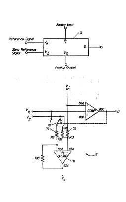
The basic SYMAD c~ll 12 shown in FIG. 1 include~
three inputs and two outputs. ~he ~ input i~ the
analog signal input, the VR i~put is the reference
vol~age input, the Vz input is a 2ero re~erence,
th~ N~-- output is~a single bit~data outpu~ fdigltal
output~9 and V0 is ~the anal~:output. - - -
The referen~e voltages are as~igned a~ follow~:
Vz i5 ~ ~0 t negative value o~ the inpu~ signal.~f the input sig~a1,r~ache :V2, the d~gital outp~t
: o~ th~ converter, regardle~æ of re~olution, will be
z~ro.
VFs i8 thQ ~ull scale~ Yoltage.or ~he ~08t positive
val~e of the in~ut ~ignal. If the inpu signal
r~a~h~ .VFs ~he~ the~.digital outputs o~ the
~con~Yerter will all be logic high regardles~ of
r~o~ution.
,W,,O,,g2!22961.,....,,,,., Pcr/uss2~0f~ss2
2 ~ ) r5
For the ~nitial cell ~MSB) VR i~ de~ined as the
midpoint betwen VFs and Vz. V~ of a succeêding
cell i8 half of this value, and 80 on. Thus, the
refer~nce voltages are w~ighted binarily. I~ the
gain of the SYMAD cells are ~et to two, then VR of
all cell5 i~ the same and reflects:
V full scale ~ Væ
VR
:
FIG. 2A shows a bipolar SYMAD cell. For some
applications,~ Vz may:be coupled to ground or to
some predetermined voltage potential. The analog
input signal VI ~i8 coupled to the non-invert~ng (~)
input 80a~ of~the~co~parator 75 and the reference
volt~ge V~ i8 coupl d ~to the in~erting ~-) input
80b of~the comparator~:75. ! The nnn .output 80c of
the comparator~:7s ls~a::.logic one when the analog
input ~signial~ is greater-~than the r~ference
voltage~ ;..jfThe nDH ~output 8ac, ~in addition to
being: coupled~-~.to an-external device, i8 coupled to
.a;contro.l;:term mal~of.. a:single pole-do`uble throw
(sP~ ;.witch~ or..~:relay ~81. ~ ~é -switch `81 has
:terminals~coupled~to the~ # ferenoe vofltage ~R and
to:the ~ero~re~erence Vz. Thus, switch 81 pas~e~
ei~her the referencel~voltage VR or the zerQ
reference~ to~R77,~ depending on the logic level
of:..the..nDn~output:~80C. ~me analog input signal V
is coupled~;.to~R79~
The ~pera~ional~a~plifier (Op-A~p) 76 preferably
has a low offset current, low offset voltage and
wos2/~2~6l . PCTiUS92/04892
~lil'l'~.~
14
low bia~ current drift. One suitable operational
amplifier with these characteristics i8
manufactured by National Semiconductor and i8
referred to as an LF 411. The Op-Amp 76 in FIG.
i~ configured as a differential ampli~ier having a
gain of two.
A typical value for resistors Rll and R13 is 100K
ohms, while R10 and R12 are 200X ohm~.
The gain for such a con~iguration can be expressed
as:
: VO = Vl[R12/(R12 + R13)]r(R10 + Rll)/Rll]
+ V2tl-(R10 ~ Rll)/Rll~
~ +:Vzt(Rl0 + Rll)/R10]tl-R12/(R12 + R13)~,
: ~ ~.where. V~ the input:; 8ignal coupled to the
non-lnvertln!g~(+~ terminal 85a: of`'thë Op-Amp 76
through resi~tor::R13 ~and V2 ~ the input signal
, coupled~to ~the~ verting::ter~inal (-) 85b of the
Op-A~p~76 through Rll.^~-. Since,~for this embodiment,
.R10 is equal to twice~the-value:;of Rll, the gain of
,r the:~,Op-A~p~?6.-is.~two,:~ and the Op-Amp's output VO
r, ~ 85c~ Q njbe expressed a~
- c ~ : V~ = 2 (Vl~-V2)+Vz .
: .. .. ~ m e~ accuracy~ ~of:~the differential amplifier is
i~proved if: 1%:~:tolerance metal f.~lm resistors are
:used~and if the op-amps' offset null is zeroed by
~conven~ional methods.~. - :.:
i ~
WO 92/22961 Pcr/us92/o4892
2 ~ 5
When the "D~ output 80c is a logic one, the switch
81 pa85e8 the re~rence voltage ~R to Rll. For
this ca~e, the analog output 85c of the Op-Amp 76
is expressed as:
Vo -- 2 (~I--VR~ +~Z '
I~ Vz i~ grounded then the output i8 ~xpres~ed ~s:
Vo = 2 (VI--vR) -
When the "D" output ~5C i8 a logic zero, the switGh
81 passes the zero reference Vz to Rll. In this
ca~;e V ~ ~r and V -- V The output o~ the
Op-Amp 76 can thus be expre~sed a~:
-:; Vo -- 2 ~Vl--V2 ) ~z ,
r ~ VO 5~ ' 2 ~VI ~ tTz ) + Vz, and
Vo ~5 2~ z!t O:t' 2VI~for Vz grounded.
~rhe ma~hematiaal expr~s~ion d~ining th~ op~ration
of the bipolar S~D aan: theréfore be expre~sed as
VO ~ ~ 2 tVI j-^ VZ - d (V~ -Vz ) ] ~ Vz ~
2(~ + ~R) ~` V~ ~or d-l, or
2~ vz - for d-0,
where ~D" ~ igi- the~~ dig~tal ~utput OI th~ s~aD cell
and -d-l ~or~-D=logic: one- and d=0 for D=logic zero.
Figure 2B shows a detailed ch~matic: of a unipolar
SYMAD cell. ~
WO, g2/~961."...,~ i PCr/US92/048g2
21111~ 16
This cell i~ ~im~lar to the bipolar cell, except
that the zero reference is coupled to ground. ^The
Op~Amp 2 has a gain of two. A typi~al value for
resi~tors R1 and R2 ~i lOOK ohms, while R3 and R4
are each 200K ohms.
The mathematica} expre~sion defining the opçration
o~ the unipolar SYMAD cell i~ expressed as:
Vo ~ 2(VI - dVR),
c 2(VI -VR) for d = l, or
c ZVI for d = o,
where "d" i8 related to digital output o~ the SYNAD
cell, a~ be~ore~ .
Figure 2C shows a: Dual Op-Amp Bipolar SYMAD cell.
In this ~bodiment,~ two amplifiers are u~ed, each
ha~ing a galn~o~two. The ~irst Op-Amp 60s has an
: 1 ~VI VR) + Vz, while the second
Op-A p~ 600 has~an o tput~ Vo2 = 2VI:- Vz. Both
outputs ~are::coupled :to switch ~10 inputi. The
switch 610~ ~:i8 ::controlled by the digital output
s1gnal~of the comparator 615~ A logic one digital
signal causès the~ ~w1tch 610 to pa~si Vo2 to the
analog output~terminal, and a logic zero c~uses Vol
to be coupled to the analog output ter~i~al. In
thi~f~ ambodiment,::~the.-settling~. time~ of the
operational~ampllfiers is not dependent :on the
outp~t of the comparator 615 or sw~tch 610. T~is
reduces;the ;total~propagation delay of the analog
signal through the cell, decreasing the-time it
wo,?2/ng6l ., PCI/US92iO4892
211110S
takes a s~cond cell (not ~hown~ to receive the
analog output signal fro~ the previous cell.
For the embodiment~ discussed thu~ far the analog
delays are a~ follow~:
ÇonfiqU~iQn Pel~Y_L~h~~ D~ =sl5fLlLut)
Figure 2A, 2B Tsa ~ Tsw + Tso Y TD
Figure 2C Tso ~ T
D
This is true for T o > Tsc + Tsw, which i8 normally
the case.
Tsc is tbe settling time of the comparator, T~w is
the witching time o~: the switch, Tso i5 the
operational amplifier~settling ti~e, and ~D i~ the
total propagati`on: delay-;~from the time the analog
input ~lgnæl:~enter~ th~cell, t~ the ti~ an analog
output signal i8~ ` available at the ~utput o~ a cell.
}f the eD~bodi~ent: ~ in FIG. 2C i~; utilised to
const ~ ct an~n-bit;ADC, the conYer~ion ~ate is nTso
faster than an n-bit ADC employing the SY~AD cells
shown:in Figures~2A and~2B.~
Figure ZD illu~trate~the conYer ion delay for tha
,
: ~ SYMADjcells~of Flgures 2A~and 2B, wherein~
VR ~s ~ e re~erence voltage; ~ `
VI(t) i~ ~the sampled analog input ~ignal;
: ;:::~ D is~the diqital output;~
Vo(t):is tha~output analog signal;
Ts~ is the~sett}ing timé of the comparator;
Tsw i5 the switching time;
.
::
WO 9~/22~61 PCr/USs2/048s2
21111~5
18
Tso is the op-amp settl ing time;
~a is the sum o~ T~w ~nd Tso; and
i~ the total delay from signal input to
table output~
For the S~AD cell o~ Figure 2C, TT is reduced to
Tso, the op-amp ~ettling tiI~e.
FIG. 3 illustrat~s an n-bit ADC utilizing a
plur~lity o~ S~MAD aells. In thi~ embodimellt, the
St~aD cell~; 12 are d~picted a8 C~5I~ 1 tc~ CELL(n)~
The analog input signal, after being processed by
conventional ample ~nd hold circuitry lo, i5
coupled to tha ~nalog ~ nput of a ~ir t SYMAD cell
12 (CEI.L 1). VR, the reference si~nal inp~t o~ the
first :S~D eell 12,; i~ coupl~d t~ the output of
the divide-by-two circuit 11~,. The output ~ignal of
divide b~-two ~ circ:uit: is - VÆF;, which is
~pr~ssed as ~
:
.
.
V~F (~ (~FS ~ Vz ) ~2 ),
wh,~r~ ; th2 :~Eull: ;cale~ voltag~, zmd Vz i8 the
zero refarence. ::
8i~o~;,~r~ aoupled~:to tha ~: ~erminal~ ,~f S~AD
cell 12~ VR -- YREF~ i If V i~ coupled to ground,
en ~R i~ ~XPre8~ed~ ~ a5
; ~ .. r ~ ~J ,` , ~
VREF = YFSj2 1,!
In FIG. 3, t:he:5 zero reference Vz 1 . coup~ed to
ground. : ~
W,,0~2/2296l .~ f PCT/~S92/~489~
211~13~
19
The "D" output of the first SYMAD cell 12 is the
most significant bit (MSB) of the digital ou'~put.
~he analog output of the ~irst S~MAD cell 12 is
coupled to the analog ~ignal input of the seaond
SYMAD cell 12 (CELL 2). SYMAD cells are serially
conn~ated in this manner to achieve the required
number of bits of resolution.
For example, to achieve a rQsolutlon of eight bits,
eight SYMAD cells 12 'are employed. This
configuration can be realized o;l one monolithic
substrate, as illustrated in FI~. 15, thus a~oiding
the complexity of using discrete components. The
conversion time for the configuration of FIG. 3 is
a linear ~un tion of the number o~ output bit~ and
is ~xpres~ed as
~ -. , . . . ~
,,.;, ~ ~ Ct ~ nTcd,
:~ ~ where n i~ the number o~ SYMAD cells and Tcd i~ the
: conversion:delay,: which iæ the sum of Tsc + T~w
Tso.
e~S~MAD cell in FIG.-2C i~ utilized, then Tcd
"~ FIG. 4 illustrates.an embodiment' wherein ~ SYMAD
,c;~cell ,12 ~ ~ utilized~'to construct ~an n-bit ADC,
: ~ ~,, wherein ~he referenae voltag~ uccessively
,~"divided by two~,before- being 'couplQd to th~ next
S~M~D stage. ,:The zero reference Vz is coupled to
. ground. In this embodiment,, th~ gain of the
differential ;amplifier within the 8YM~D cell is
WO 92/22g61 : C7 PCl'/US92iO4892
-- .
211110~
adjusted to unity to accou~t for the successive
division o~ the re~rence voltage. As many SYM~D
cells as nece~sary are ~mployed to achieve the
desired re~olution~ R~æistor networks are ~uitable
for implementing the divide-by-two ~unction o~ the
reference vol~age~ Du~ to the divid~-by-two
networks, ADC realization i~ more compl~x ~,han the
con~iguration ~hown in FIG. 3, how~v~r, the
conversion time ~or th~ FIG. 4 con~igura~ion is a
logarithmic function of th~ number ~ output bits;
and i~ thus fa~ter than the conversion time ~or the
FIG. 3 configuration~ The equation go~erning the
output voltage of ~ach cell i~ VO = VI - d(VR-Vz).
A Cyclic Analog to Digital Converter i8 illu~trated
in FIG. 5. The correspondi~g timing diagr~m for
this con~iguration i~ ~hown in FIG~ 6. In this
embodime~t a aontr~ller, such as a microco~puter
14, output~ a clock ~ignal to a first ~amplQ ~nd
hold circuit l5.~:Th~ ~utput of the ~ample ~nd hold
15 is coupI~d to~the analog ~ignal input t~rminal
of the S ~ D cell 12. The reference æignal YR, o~
the SYN~D cell~l2, i~ the æu~ f VFs ~ Vg divided
by two~.. The~divide-by-two function is p~r~ormed by
th@ diYid~ by-two n~tw~rk 18. The zers re~.rence
Vz is coupled~to~ground, ~herefore V~ = VFs~2. The
~D" output of the~SY~AD.~cell 12 i8 coupled to an
input of~he~:icrDco~putQr 14. ~ Upon ~he recept~on
o~ thi sing~ ~it~fro~ the "D" output`port o~ the
SYMAD cell 12, the~icroco~puter 14 ~mits a s~cond
clock pulse which~i coupled to a second sample and
hold circuit 17.~ The analog output o~ the SYMAD
cell 12 is coupled t o the input port of the second
~1yO g2/22961 PCr/lJ~i92/04892
2111 1~5
sampls and hold circui~ 17. Th~ output of the
sample and hold circuit 17 i8 eoupled to one oP the
terminals o~ swits~h 19 . The analog input ~i ~ gnal i~
eoupl~d to ano~her input taxminal of ~witch 197
The eommon t~rminal of ~w~t~h 19 is eoupled to the
input of the ~irst ~ample and hold eireuit 15.
The ~iieroeomputer 14 emit~ a switeh eontrol signal
20 that dQtex~ine~ whioh sigllal, the output o~
~ample and hold 17 or ~he ~n~log input t3ignal, i8
eouplad in~o the input o~ sa~ple and hold 15. The
analog inpu~ signal i8 pa~ed through the switeh 19
to the lnput o~ the girst sample and hold 15 at the
beginning of the f irst eomrersion . q~he output of
the seeond sample and hold 17 i8 pas~ed through the
switeh 19 to the ~nput of the ~Eirst æample and hold
15 ~or uaeessiv~ eonversion~ Thi~ Al)C
eonfiguration ~i8 trery ~imple ~nd, beeause Q~ the
low parts~ colant~ can ^ b~ ~ad~ ~xtrs~ely accurate.
Thi~ ADC conf iguratio~ readily cap~le of
per~orming 16 bit conv~r~ios~ or more. A
se~enaer, or any other device capable si~ produc:ing
the waveforms shown in l?IG. 6, can be substitu~ed
for the ~icrocompu~r.~
, .. .,...~
Re~Eerring to~ ~IG. fi, the . rii~ins ~ edge e~f clo~k 2
app~ars, ~t a ti~e S +,; C .:after..~he? ris~ng édge o~
610ck i, wher~ S = s~ttling ~i~e '~ ! of ~ sa~aple and
hold circui~ and where a i- analog ~ettling time of
~e ~AD cell.
In Figure 6, the analog input si~al, after b~ing
processed ~y the ~ample~ and hold, ~ettle. at point
A., T8c i~; the comparator settling time, Tsw is
WO 92/22g61.~ . PCr/US92/~48g2
~11105
22
the switching time, and Tso i~ ~he op-amp s~ttling
tim~. The analog outpu~ signal ~ettles at point B.
~sc i~ the comparator settling time, Tsw is the
switching time and ~so i8 the op-amp settl~ng t~me.
Conver~ion t~mes o~ ane microsecond per bit or
~aster are achieved ~ high speed analog part~
~operational ampli~ier and ~ample and hold~ are
utilized. Conversion times of one micro~econd per
bit enabie ~he ~DC to ~ake 60,000 16-bit
conversions per -~econd. This co~v~rsion ra~e i8
suitable for use in aompact di~k record~rs ~nd
other appllcatlons r~quiring high ~peed aontinuous
conversions. Bene~icia~ly, thi~ embodiment
provides a high ~pe~dL A~C that require~ but a
single cell. ~ As~a re~ult, increased accuracy is
obtained beaaus~-o~ a reduction in the ~verall
pa ~ ~ count-~ relativei~to a co~parabl~ n~bit
co~verter baving~:n-cell~
During op~ration,~icro~omputer 14 accu~ulates the
suc~es~e digi~al ~U~pUt8 for each conver~ion to
any d~sired nu~ber o~ bits:o~ rësolutionO
G. 7A illustra~es~ ycIic ADC emplQyin~ chopper
stabilization.~ Twot~chopper stabi~z~d`~C~ axe
u ed in ~uch a-~anner:~that while one i8 conv~rting
~a s~mpled~.analog:signaI~into a digital~outpu~, the
other AD~ is in a~zeroing mode. On a ~irst clQck
pu15~, an analo~ input signaI i5 ~ampled, thus
b~ginning the~ con~ersion proces~. F~r all
rem~ining cIock pulses, until the desired output
bit resoIution is achieved, th~ remaining
WO 92/22~(1 . P~iUS92io4892
S
23
conversion~ are ~ade on 1:he analog output ~ignal
fro~ th~ syNaD c:ell that i8 fed baak into ^ the
circuit. In the corl~er~ion mo~, on~ o~ the irlput
ter~inala~ o~ spD~r switeh 98 i coupl~d to thQ
anals~g input ~:Lgnal. q~i~3 ieS accompli~h~d by
microco~apuker 14 ~itting a lsJgic on~ signal on
I~lput/F~edback line 100. The analog i~lpUt ~ignal
pa~se~ throu~h Switch 9~ and ~ coupl~d to an ~s~put
terminal o~ SPD~r switch 96. A logic: on0 emitted by
microc:cs~put~r 14 on th~ Con~fert/Zero lin~ ,, which is
coupled to the control terminal o~ swi~ch 96,
caU8es the analog signal to pa~s to the 8u;~irlg
ciraui~ 94~ The ~u~ing circuit 94 ~3ub~rac:ts an
o~fset voltage, produced by the integrator g5, from
th~ analog ~ignal., ~e r~sulti~g si~nal i~3 coupled
to the iJ~put o~ ~mp}e and hold 93,. q~e sampl~d
a~al~ ~ l at th~ ~utput o~ ~a~ple and hold 93
i~ th~n c~apled to th~ i~aput o~ ~sa~pl~ and hold ~1.
~rhe o~t: oî ~ opl~ zmd hold 9~ is then coupl~d to
thQ analog input of the S~aD cell 12. Th~
ref~r~m::e ~roltage VR applied to the S~LaD cell 12
i8 ~xpre~s~d as:
~ ` ` Y~ (~FS Z ) ~ ~
where ~z i ~ ~he Z~EO r~erens::e volta5~e and VFs i~;
'che ~ull ~cale ~rol~a~yQ.
h~ z~aro reference; Vz of S~qAD cell ~2 may be
.
coupled to grourld . For t~ a~;e ~ ~R i~ expre~;sed
as:
R VFS/2
~0 92/22961 - c PCr/US92/04~2
21111~5
24
The analog output o~ the s~rMAD cell 12 i~; coupled
to an input texminal of ~witch ~2 and o~ witc~ 9~.
When the Input~Feedb~c}e line, which is coupled to
the con~xol terminal of switch 9~, is a logic zero,
the SYMAD cell 1~ analog output signal i5 ~ed back
into the ADC: as an input and the ext~rnal analog
input sigrlal is not used. The ~witch 98 no~, pas es
the SYMAD analog ou~put signal to an input terminal
of switch 96. Since the ADC i3 in the conversion
mode, ~;wit ::h 96 pass~3 the SYMAD analog output
signal to the input o:E the summing circuit 94. The
inpu~ to the integrator 95 ~s the zero re~erence,
there~ore the output of the integrator 95 is
unchanged.
Thi8 ~ode o~ operation continues until the d~sired
nulaber o~ bit~; arQ accumulated for one conversion.
~t this ti~e, the~: ~iræt ehopper ~;tabil;lzed ADC iæ
placesl into th~ zeroing~ m~de, designated by
microcomptlt~r 14 emitting a lDgic zero on the
Convert/Zero line.
~; . . - ..
A logic z~ro on the ConYert/Zero line c:au8~æ 8witch
96 to pa~ ~he: z~ro~ raference to the input of the
~ing aircuit 944 Al o, the ~;econd chopper
~tabiliæ~d ~D~ 12 en~ers the c:onYersion mode.
Referring to FIG. ~7C~ the *ir~t chopper stab~ Qd
ADC take~ sample ~ A, ~ and ` at ~th~ end of period Tl,
durir~g which ~ime the ADC i8 in lthe feedback mode,
ît produ ::es an n-bit conver ion. SaiDple B i~; taken
by the s~cond chopper stabilized Al)C w~ile the
f iræt c:hopper stabil ized ADC is in the zeroing mode
WO 92/2296l !~x PCr/US92/04892
2 1 ~ S
(represented by a logic one s~gnal on the
convert/zero line) . ~ -
The ~ir~zt chopper stabilized ADC produce~; sample C
at the end o~ T2 ~ whi:Le the seaond chopper
stabilized ADC is in the zeroing mod~. When one of
the chopper ~;tabilized ADC's is in the zeroing
mode, its digital outpu~ i8 ignored by the
aicrocomputer~
l~uring the zeroing E~hase the ~icrooomputer holds
both ~3ample and hold circuits in th~ sample ~tate,
and sinae all ac'cive components are in 3eries, the
ADC provide~ rOr ~h~ nulling o~ all oi~8et8
simultaneously. The integrator 95 per Orm5 a
null~ing function wherein the o~ ~t~; produced by
the ~u~ing n~twor~s, the ~aallple and hold cirauit~;,
or t~ae~ di~fer~n~ial aDIpli~ier i n lthe ~3Y~aD céll ~re
.,. ~.......
~ffectively nulled out by the intes~ra1:or 95 output.
Tlle following exa~ple, wherein one ~illivolt
o~fsets for each~ device are asslamed, illustrates
the alullin~ function~shown ~n FIG. 7D. If a one
~illivolt~o~ et~ F~ produced by sa~pl~ and
hold,~9vp3, .~henl-at~poin~ B, whiah i8 ;~h~ ~nput to
~a~le~and~hold~9~, there~appears a ~one ~illi~olt
ignai- S~mple~and~hold~l al~o~produces an o~ et
voltag~ (VOF~ at i~ output; th~re~ore ~he sig~al
at point ~.- i8 ~xpr~s~ed as V~2 ~ G Vin~ w~re G i8
the gain of the sample ~d hold 91, ~hich i~ unlty,
and Vin i the input ~i~nal to ~mple and hold 91 t
which i~ equal:to VOFl (VI i~ coupled to ground,
therefore Vin is ~qual to the offset voltage of the
precQding staga). The magnitude of the ~ignal at
WOg2/2~g61 PCT/US92/04892
21111~i
26
point C in FIG. 7D i8 equal to VOFl + VOF2, or two
millivolts.
The SYMAD aell 12 has a gain of two and also
produces an offset voltage, VoF3~ of one millivolt.
Therefore, the output of the SYMAD cell (point ~)
i~ expressQd as VO = 2(Vin + VoF3), - in
the ~um of VOFl and VOF2. Thu8, the magn~tude of
the error at point D i~ 6mv.
This 6mv sig~al i& the input to the integrator 95.
Referring to FIG. 7E, the output of the ~ntegrator
9S never reaches the input~level because when an
output of 3.0mv is reached, all offsets are nulled
out, resulting in a zero level:~slgnal at oint D.
In t;e conversion ~ode,:the input`to integrator 95
: ~is zero. ~A~zero ~lnput to~an integrator will not
c~ its output, .therefore-the'~:integrator 95 i8
~aintained at a 3:.0mv output.~
A~further~ i~provement~ employs the zero/¢onvert
signal ::to ~-:electronlcally~ r~ ove~-the feedback
resistor~;of:the:~SYMAD~dif~erential;amplifier during
the~zeroing-~ph`ase.~ Thl :~-e * ctlve~y ~agnifie~, to
8 ~ atlon,~the S~error ~ signal' ~ ~ o~e ~ idé~`any input
offsets~.af~the~ integrator.~ Thus~ an inéxpensive
JFET, amplifer,: ~havlng ~a..r~lativ~ly high input
of~s~t,~may~be~used to~onstruct;:the integrator 95.
A~urthe~mbodiment~ of:-the-~;:lnvention utilizes the
SYMAD~;cell~ 12~ in~ a Pipelined~:Analog to Digital
Converter,~as shown in FIG. 8. Be~ween adjacent
:SYM~D cells 12, t~ere are provided two sample and
:
: ~ :
'W09~/22961.,s PCT/US92/04892
21111Da
hold circuits, each being controlled by separate
clocks produced by a clock generator 43. ~~The
sampled analog output of the ~rst SYM~D cell 12
(CELL 1) i~ shi~ted by two sample and hold circuits
28 and 2g to the analog input ~ignal termin~l of
the ~econd SYMAD cell 12 (CEL~ 2). While the
~ampled analog signal is shifted by the sample and
hold circuitry to the second SYNAD cell 1~ (OELL
2), the first SYNAD cell 12 (OE LL 1) recaive the
analog input signal ~rom sample and hold 21. The
edge-triggered clocked D-flip-flops 24-27, 31-33,
37, 38~and 42 each provide a one clock period delay
such that the cvnverted blts o~ a partiaular sample
arr~ve ~t:the~digital output~ simultaneously. The
pipelined analog to dig~tal converter shown in FIG.
.
8 beneficially~provides:a rate of conver~ion that
i8 constant~ regdrdless~of~the number of bits bQing
converted. That; ;iB~ once ~the pipeline i~ filled,
ever~ clock~pulse~:yields~ an ~n-bit digital output
repre~nting~a~prior ~sampling: of the analog input
signal. Fu ~ ermore,~ the configuration ~hown in
FIG.~8 may~be:~expanded :with :additional converter
tageæ:~without~:degrading~the~onvers~on rate. The
C91~erSiO,n~ t~ may. be~ eYp#88ed ia8 one ovër the
com/ersio,n,~ .period ~
The conversion! ~ period is express~d as (2(8) ~ C),
where.~S ~-s~4~theA~et~ling:time of-a ~amplé`and hold
circuit, and~wheré:C~ ,the`ana:log settling ti~e of
he SYMAD:cell~12.-
~
:
:: :
: : : :
:: :
WO 92/22961 ~ ,~ PC,T/US92/04892
2 ~ 3 ~ 28
The pipelined analog to digital con~erter alsoinclude~ an analog delay fun~tion. The analog
delay through the pipelined ADC i8 expres~ed as
Analog conversion delay = nt2S ~ c)
Figures sA through 9E illustrate the ~pplic~tion o~
SYMAD cells to co~pres~ion type convertersO wherein
compre8Rion i8 con~idered to be baRically a
10garithmic:function~ There are two ma~or types of
compression that are considered herein: log2(x) and
log2(l~x), where "x" i8 the input ~ignal and the
ba~e of ~hie log function ifi 2. Log2 (~+x)
co~pre~sion may be employ~d for the compre~sion of
audio ~ignal8 ~or telepbone 8y8tems a~L sound
~f~ct ~ystems, ~in ~that it lends its~l~ to ~he
oharacteiri~tics of the~ huma~ earO ~og2(x)
co~pre~sion, as wi1I bs seem 1ater, - can be e~plt~yed
as part;~ of a direct reading floa~ing point ADC that
meets the ~ ~loating~ point; . repre~entatior~ u ed by
processors,~; ~such: as the National Semiconductor
NS32081 ~ floating point~ ~proc-~sor.
T,o, aid~ the~ d~scription o~:~ ,SDQ~D^ compression~ cells
~veral~ definition~ ~re first~ establishéd~`. ;
One~,of the~o t important-definiti~nF ~8 that of a
UNITY. ~ reference. This~ intended -to ; mean an
a~nalcg;~ voltage :that r~prese~nts unity, or the number
1. Th~ valué o~ UNITY is ~easur~al with respect to
Vz, the zero referenc:e . The next def inition is
that of a ~SE reference. In that the ba~e of the
logarit~ic conversion is two, base is def ined to
WO 92/22961 PCll /US~2/048~2
211110S
29
e~ual 2, or twice unity. It ~hould be realized
that in accordance with the foregoing tha~ the- same
principl~ can be employed to create a c:om~ression
converter of any ba~;e so d~siredO
First, log2 (x) compres2;ion iE~ di~cus~Qd, I:y an
app~ication of thi~ technique to log2 (l~x)
compre~sion.
IA~garith~ic compressiorl is ~e t describ~d in the
context of binary floating point arithmekic. Gi~en
a binary inte~er that i8 to be convert~ to
floating point (for example OlOllllllO), the
~ntQger i~ ~irst written in the ~or~:
~)101111110.000~0000 X 2~).
The loating point rule~ di~aus~;ed abQve rQquire
t:hat ~h~ ~an~ a be between 1 ~inclusive` a~nd 2
(exalusiv~), thu8 t;he manti3sa i~ shifted to the
right enough tiD~es 80 that the ~ost signi:Eicant set
bit i5 tG ~he left. o~ the binary point.
rrh~ shi f t right . operation i~; ~q~ivalent: to division
~` ~by 2~ HowevQr,: in:l.o~rd~r to~ ~aintain;th~-.;int~grity
~of the ma~itude, .1:h~ e~pone~t; JI~U8t: ;A`3be inGre~l~!nt~!d
by one I~or eal:h righ~ward shift per~orm~d. - ~hu~,
the outco~e~
1:. 01~1111 X 21.
'
For purposes of ~;y~etry ~ralueg that are le~s than
l may also b~ compressed by ~ultiplying the
w~92/22s6l ~, PCT/US92/04892
21~11U~i
mantissa ~shifting left) and ~ubtracting ~rom the
exponent.
The value 0~000 ~binary) i8 equal to the int~ger of
khe log~rithm (to the base 2) of the original
binary value given above. Thi~ exponent, by
itself, i8 the desired output of a loga~ithmic
compression ADC.
~he abov~ described technique lends it~elf to a
cyclic conversion process, discussed below, in
order to rapidly perform the logarithmic
~ompression.
.
A set of mantissa multipliers are de~ined that are
: weighted to the bit positions o~ the exponent, such
that a single:S~MAD cell is assigned p~r exponent
bit.~ For eYa~ple~
~ 2~
l~= 4 =:l/4
200100~ 6~= 1/16.~
In~ accordance~ with ~the foregoing, to përform
~logarithmic~co~pression there iæ dëfinèd a~ list of
thresholds~ T(n),;~ multipl1ers Q(n) ~and binary
., exponent e~uivalents ~Brn)-. Thus, the followin~
table is presented~
'
WO 92/22961 . Pcr/uss2/o4892
21111~S
n T(n~ Q(n) E(n) B(n)
-5 ~/256 512 -9 10111
-~ l/16 32 -5 11011
-3 1/4 8 -3 lllOl
-2 l/2 4 -2 1111()
~. .
-1 1 2 -1 11111
2 1/2 1 OOOol
2 4 ~/4 ~ ~ 2 00010
:
. 3 16 1/16 4 ool~o
4 256 ~ 1/256 ~ 010~
where~ ~ T~n) is~ a threshold v~1ue (th~ voltage
r2ferent:e used: for compre~;ion is
Vr (n) ~U~aITY~T ~n) ~ol~s~
Q(n) ~is;~e~ mant1ssa~ u~tiplier~
:
.~ ,13(n) ~;is what is added :~o th~ exponent to
of~set :the effes:t ~of the ~ultiplier:
3(n)-1og2 ~VQ(n) ]~
B(n) is the t~o~ compl~ment equivaleT2t to
E (n); and
:
: ' :
:
WO 92~22963 PCr/l~s~/0~892
21111U!~ 32
n ~ the order o~ the output bit, where n=1 i~3
the LSB for a natwork of LD cells, and
n~-l i8 khe LSB for ~ n~twurk o~ LM
c~lls .
The table may be expand~d by ~ollowing the paktern
shown . T (n) above th~ table lin~ i~ a value that,
when ~ultlplied by Q (n~, r~sult~ in 2 . T ~n) below
the lin~ i8 a v~lue that, when ~ultiplied by Q(n),
result in 1~
A descript~on o~ the use of thi. Table i8 now
provided .
&ivell an analog inp-at vol~age V a~d a 3;bit log2~x)
co~pression æystem:
1 ) ~lear a result r~gisker;
2~ if Y~ 33 ~n Y:-~*Q(3) and add B(3) to
result;
3) if V>CT~2)~ then V:=V*Q(2~ and add B(2) ~o
r~sul~
4~ i~ V~T(~ then ~V:=~*Q~ and add B(l~ to
result; ~
S) if ~V<T~-3): ~en V:-V*Q(-3)C~ and add B~-33 to
r~sult ;~
6) if Y~T(-2) then V:=~*Q(~2~: and add B(-2) to
result; ,.
,, ~ , . . O
7) if KT(:-l) then ~V~ *Q(-l) and a~dd B(~ o
resullt; and
) end .
W~, 92~22961 . . ~ PCr/US92/04~2
~11110~
The ~inal value of V may thus be applied to an ADC
~o obtain the manti~;~;a, as described aboYe ~ ~while
the result regi~;ker contain~ the exponent. The
exponent may also be considered a IN$(log2 (V) )
aompression on the input voltage.
Figures 9A and ~B are~ block diagra~s ~howing two
basic cell types for producing ~traight logarithm~c
conv~r~ion. FIÇ;. 9A ~how~ cell with an "I~
de~i;ignation. This c~ a logar~ ic d~viding
cell; a cell used ~or compre~E;ing voltages greater
than 2*UNI~Y. The ca3ll designated as ~ in FIG~ 9B
i~; a logarithmic mt%ltiplying c:ell; a c~ll used for
compr~ssing vol~age~; le85 than UNITY.
The ~ath~atical equations that govern the cells
are~
L~ typf~:: Vo = (l~d~*Vi*~2(n) ~ d~i; and
.
LD ~ type: Vo ~ [l-d~ *Vi ~ d*Vi*Q~n);
where - d=l for D=logic high,
~lse ~=0, ~ t; ~ " -, ~ ". ,r ~
Figure~- 9C ~hows -a -realization for both IN i~nd I,D
~rpe .;¢ell~, ~ th~ only: diff~rence between the two
~mbodi~ents~i ~the orientatiorl o~ the sw~tch (~;W)~,
as wi~ other. S~D ceIl~ d~scrib2d pr~iou~ly a
comparator c~apar~s an input voltage Vi to a
reference volt~ge~ Vr. If Vi is greater than Vr
then a logic l appears at the D output. The D
output is f~d back to the control irlput of SW to
WO 92/22961 PC~/US92/04892
21111~5
34
select the analog output. Therl3 are two possible
c~ut:l?uts that can be txan~laitted to the analog
DUtpUt, one being the input voltage through a
voltag~ ~ollower (V~), the other being outpult by op
amp (OP) as a product of the input voltage with a
constant that i2~ a function o~ the order o~ ~he
output bit that the part1 cular cell repre~enits . In
the Ca89! of an I~D type cell, the product path ~s
selected when the nD~ output i8 hig~, ~lse the VF
path i~ ~;elected. In the case of the LM cell, the
VF path i8 ~elected when the "D" output is high ~
else product path i~; ~elected. The reference
voltage V~ 3 also a ~w~ction o~ th~ cell order and
i~ a voltage equal to T(n~ *U~ ITY. ~rhe zero
referer~ (Vz 3 i8 used to set operation in the
bip~lar mode~ For ~in~plicity, ~z i8 ~et to ground
for desoription purposes.
Figure gD ~ shows a log2~x) compres~ion: A~C. ~his
co~v~rtar pro~uces bo~ po itive and n~gative
values, where: a binary output OI 0~11 i8 z~r~, 1000
is ~ and 0110 i~ -1. The output can be eonverted
to two~ ~:om~liment ~ by s1abtract~ng 0111: fr~m the
output,: however,~ the r~presentation as pre;ented iæ
con~tent with the~ ~ormat in which floatit g point
processors repres6~nt: exponent~. - Thi~; ~c~nvërter can
be c:onstructed to n-bits ~y 8~111ply- ` following the
pa~tern sIllust~ated. This diagra~ ssu~es that the
inpu voltage is stabl~ while c:orlYerting.
Comparaltor csD and switch SW9D select the
appropriate mantissa source for the mantissa
output. If the input voltage is less than unity
WOg2/22961. PCT/US92/04892
21111~S
the analog output of the LM o~ converter cells is
selectsd. If the input voltage i~ greater ~than
unity then the analog output from the LD chain of
con~eter c~lls i8 ~elected ~or mantis~a processing..
The voltage reference ~or the compr~sion ahains
can be derived a number o* ways, how~ver the
pre~err~d m~thod employ~ a low input o~fset op-amp
OP9D and divid~r network~ DV1-DV5. The output of
the div~er n~twork~ ~V2, DV4 and ~V5 generates the
UNITY referenoe, which i8 the fed back to the
invert~ng input of the OP~D. Thus the user need
only ~p*ci y what voltage will r~pre~ent UNITY into
the non-invQrting input to ~h~ OP~D. Th~ digital
adder (DA) 8ums both th~ negative and positive
co~ponents of ~he exponent to generate the
composite~xponent. ~ `
Figure 9E illustrates~ an exa~ple o~ ~ow the
co~pression ~ C of FIG. 9D ~ay be employed to
r~ali2e a-~direct reading, floating poin~ analog to
digital converter. An analog inpu~ ~g~al ~s fir t
proc~ed~by a sample and~hold circuit ~SH~s th~n a
co~parator (C9E~ d~t~rmi~s if the i~put ~iyn~
positive or neg2tive. The ou~put of the c~parator
C9~ i~ dlrectly~;us~d as ~hé~ma~ti~s~ sign, as w~ll
a8 b~ing used to control an analog switch ASW to
sQleet either~an-i~Yert~r~ or a ;~ollowèr (F) to
r~ctify ~he signal to the log2(x) ~o~p~s5i~n
~on~ert~r.~ (CC), as depicted in FIG. 9D. The
digi~al output :of the l~g2(x) con~erter is u~ed as
the floating point expon2nt ~while the remaining
outputs ara connect~d to an external ADC to pro~ide
W,0s92/22961 ~, P~T/US92/0489i
2~1110~
36
the mantissa data. The signals may be conn~cted to
a standard cell n-bit converter or a ~witched
resistor n-bit ADC (of a type de~aribed below),
however any ADC may be us~d ~or thi 8 purpose,
wherein ~he UN'ITY re~erence output i~ the lower
conversion limit and the B~SE output i8 the upper
conversion limit.
It should be noted the ~anti~sa ~utput includes
only tbse fractional part of the mantissa. This is
because the mantissa output of the compres~ion
converter normalizes the voltage between UN'ITY and
~ASE. Thus, there i8 an implied 1 to the left of
the binary point. This i~ consistent with the
floating point representation mentioned earlier.
Figure 9F ~hows a log2(1+Y)~ c~mpr~ssion anal~g to
digital converter that i~ realized with LD type
compression cell~ only.~ Th~ x) ~feature i8
raalizQd by addlng th~ UNITY re~erence to the lnput
: signal of the fir~t cell. The input Yoltage range
of ~ this ~ co,merter~ fro~ Z to
UNITY*(2n~ ~ ITy~volts.~ The binary~outpu'r of th~
converter :is~defined9as-~ r 'i, ', `''~
: ~::bina ~ ogtput=INT[LoG2(uNITy+v~)]~
wherein the lo~arithmiclf~ ction is to base 2.
: Cyciic co~pression oan be achieved by ~ubstituting
~the SYMA~ cell of FIG.~ 5 with an LD(n31) or
L~(n=-l) type:cell or with an~optimized cell of the
LD-type, as seen in FIG. 9G.
~: :
wog2/22s61 P ~tUS92~04i9~
2 l l 1 1 ~
A cyclic LD expanding circuit is realized by
~ubstituttng the SYMAD cell in FI~. 5 with a~(X2~
multiplier and connecting th~ input signal line to
the ~NITY voltage. The output o~ this expander i~
taken at the input to the (X2) network.
A cyclic LM expanding circuit i~ realized a~ above
except that the ~X2) mul~iplier i8 replaced with a
di~ide by 2 network, such as two serially coupled
r~istors of the same value.
FIG. 2E showæ a block diagram of a synchronous
SYMAD converter:cell~200 havin~ a clock input. The
synchxonous SYMAD converter cell performs a sample
and bold operation and a compare operation in
parallel, as~opposed to~being performed in tandem,
as is the case w1th:the SYNAD converter oells shown
in Figs. 2A, 2B and:2C. - -
" ~ "
FIG. 2F ~hows in greater detail a a ~ynchronousSYMAD converter cell embodiment.
Referring now~to~ FIG. 2G,: JFET vo~ag~ followers
240 a~d~345,~switch~250~ witch 255 and D-~lip-flop
210 form an~,edge~triggered~analog ~ampl~`~and hold.
Switch~250~ and~;switch i:.255~ operate ~out o~ phase,
permitting~one JFET:vsltage follower to sample the
analog input~ nal: while~ the othex ~FET Yoltage
follower holds~its:output constant~ A rising ¢dge
from~the.clock~ ignal toggles fli~-flop 210, ~hu8
toggling ~:the ~unotion of ~he JFET voltage
followers. ~: m e: :;co~pare operation is performed
befoxe the~samp1e and hold opera~ion, thus removing
WO 92~22961 . Pcr~us92io~892
~llllD5 3~
th~ effect o~- the comp~re ~unction propagatior
d~lay.
Flip ~lop 220 perform two ~unctions: (1) to
~ynchronize the arrival o~ the digital output
signal "D" to the ~;amplsd analog s~gnal at the
input to the operational ampliPier 230, and t2) to
remove any i2~3tabillty of the comp~rator 235 ou~put
that may exi~;t when ~he analog input signal and the
refere~ce signal have equal magnitude2;.
Capacitors 270 are pr~ferably of the low l~akage
mylar type. The operational amplii~r 230 is a
high speed device, prefer~bly with a J~ET inputfi.
FI~;. 2H showE~ a timing diagram of a ~ynchronou~
SYIIII.D c6!llo The clock. period Tc ~g~al~ the ~ime
r~quir~d for ~ comparator and ~ampling capacitor o~
a Rucoe~ding 23t~ge ~:o s~ttle aI~ter a ri~;~ ng edge of
the c:lock. The co~parator 235 c~utput~ the d~gital
signal "D", ~is delay~d ~only by the propagatio~
dalay of ~lip-1Op ~20.
FIG~:tl 2I~:~ shows~. a ~cyclic AE~ utilizing a sing~e
ynchronou6 SY~D - cell- and~ `:MG.:~ 2J ~ show the
,.~corre~ponding.~t~ing~diagram4: ~Thl~ :eyc:lic i~DC does
not reguire a~ sample and hold on the in~put, unlike
~he e~odilaent showr~ in -FIG . ~~ i5 t~
A: logic one on i; :the Sa~pl~Feed~ack7 line ~ CaU8e~
~witc:h~ 30Q: to pa~; the analoq input ;ignai to the
input terminal of thQ synchrc3nous SYMAD cell. A
logic zero on th~ Sampl~/Feedback lin~ causes
W, 0 92/22961 ~- ~, i PCI'/US92/048g2
21111~)~
39
switch 3 00 to couple he analog output of the
synchronoll~; SY~D cell back to the input of~ the
c~ll, thu# creat~ ng a feedbaak loop ~ ~he zero
r~erence o~ the c:~ll is pref~rably coupled to
ground. ~rhe aonversion time ~or th~ ~ ayclic ADC is
~aster than that ~3hown in FIG. S because the
~;ynchronous SYMAD cell cyclic I~DC'~ sample a~nd hold
operat~on and c~ mpare operat~on are performed in
parallel, r~ther than se~uentially.
A controllex, such a~ rocomputer 30:2, outputs
the Sample~Feedbaclc waveform, outputs the
~ynchroJlQus SY~AD con~rert~r c~ll 200 clock waveform
and r~ceives th2 cell ' g digital output signal~i; .
FIG K 8how2; a pip~lined A2C utilizi~lg a plurality
o~ synchro~ous SYN~D aonv~rter cell No ~ample
and hold ~:ircuit i~ r~g uired at the analog input
b~cause ealch ~ynchrorwus SYM~D c:ell ~ nclude~ a
sa~ople and hold runc:t~ on. Ther2~0re, the sample
and hold circuits be~ween the cells ~ay al~;o be
omi~ted. ^ ~h~ la~t stage, or I,SB, c:an bé realized
with only a comparator. All ~lip ~lops are
txigç1ered ~on the.c:lock's ri~ing edg~.- Since the
æa~ple, and hold operation and the co~pare operatiotl
c~f eacll cell~ :are parformed 'in parallel, rath~r t~an
se~uen~ially, the cc~nverqion time i~;~ fast~r than
Ehe pip~;ined ADC ~howII :in FI~:. 8.- ` ~
Another embodim~nt oP the invention i~ a switc:hed
resi~;tor SY~AD (SRSYMAD) cell showTl in Fiys. 101~
and lOB. On~ advantzlge of this embodiment i~ that
the resistor n~twork can be used in performing
W092/22961 PCTiUS92/oi8~
211~1~5
either an ~DC function or a DAC function. Other
applications of this embodim~nt include a digitally
controlled analog attenuator and a digitally
controlled potentiometer.
The chart below de~ine~ the SRSYMAD cell input and
output signals.
~TGNal_~a~ D~RI~IQe I~T~OUTPUT
VRl Positive Reference Input
VR2 Negative Reference Input
DI Digital Signal Input
Vol Po~itive Reference Output
Vo2 Negative Rererence Output
VAR~ Analog Reference Output
~Referr~n~ now to FIG. lOC, an ADC -function is
r alized by connecting a co~parator 122~ in such a
; wa~ that . the;~ VARO signal is:: coupl~d to the
i m erting t~rminal (-): 123b of comparator 122 and
the analog ~ input~: signal i8~ coupled to the
non-imerting ter~inal (~) 123a of comparator 122.
; When the~i ~ log~input signal VI is~greater than the
analog reference~ ignal~ VAhO,::~.th~ comparator 122
,; "~5 a ~ i;c~one~ ;,If the~analog input isignal VI
i8 les ~ th=an the; analog ~ reference VARO, the
comparator 12~2 outputs~logic-zero. . ~
,
: ~ The co~mparator:~l;22~ output 123c is coupled`to the D
~;ter~inal~ of~the~switched resis or cell, as shown in
: ~ ~FIG~ lOc. When a:logic one signal is ~eceived at
~ the DI terminal, the ~witches are activated such
WO 92/22961 . s s Pcr/US92/0~892
21111~
41
that the cell configures its~lf as ~3hown in FIG.
lOD. R' i8 the r~si~;tanc~ looking into ~,he VRl,
VR2 t~rminzls o~ 1:he next ~3witched resi~3tor SY~AD
cell. The analog ~witch~ wap re~istnr R ~nd the
output t~rminals Vol and Vo2, while maintaining
their polarity. When the r~ferenc:e output
termi~al~ are ~ at~d with R obm8, t:he
resistance between the input terminals is R Oh~118.
Thi~ ; t~ue whether digital input a~ignal DI i~ a
lo~ic zero or a logil:: vn~.
Therefore~ output o~ one cell may b~ ter~inated
by the input r~si~tance o~ the next cell and 'che
~inal cell i8 terminated by a resistor having a
value of ~R. The input resistance to a cell
( looki ng into ~e VR1 ~nd ~R2
e~pressed as
RVR1,VR2 -- ( (R'+R) ~2R) )/ (2R~R~R' ~ .
. . . . . .
Since R' -- R, the ~xpre~sion i8 reduced to
~ 4R2/4R =ii ~
where -R~i~ VR2 is the iripllt n3sistanae ~looking into
- .- the ~Rl and VR2 ~ ~er~inàls of the ~wit~:hed resi;tor
~ ~ S~M~D ~::e~ s-- -'rJ ; ~ -
- The ~agnitudes of ref rence vclltages VRl and VR;2
are ;el~cted by the u~er, howev~r the s~lection
aaust take in~o consideration the magnitude range of
w~ 92!2296l ; Pcr~us~2/o4892
2:~1110~
~2
the analog input signal. For example, i~ a worst
ca e analog input siynal ha~s a range of zero to
thr~ volts, then to ~aximize the resolution of th~
data output, the user may select ~IR2 3 0 and V3Rl ~
3V.
Fig~. llA and l1B ~llustrate thi~ con~iguration.
The comparator output o~ each stage sets up the
configuration for that 5:ell. This con~iguration
deter~in~ the xeferenc~ voltages VRl and VR2 for
th~ next cell.
This pattern læ r~peated for N bits. It should be
noted that the last cell :18 termina1:~d witk ~. It
i~; al~o within the E3COp~ o~ t~. inv2ntion to
con~;trucl: the l~st cell with a reæistor network a~
shown in FIG. llC.
A ma~or advantage of the ~lditc~d resi~tor SYMaD
c~ll it; thi~t it can al~o be us~d to construct a
digital to analog converter. The comparator
airc:uitry i8~ ~not needed for t3~e l)AC ~unction. FI~;.
~2A 6hows ~ a thxee bit r~c u~lizin~ three switched
resistor S~AD c:ell~;~ in the DAC mode.
, ,~
~h~ valu~e~s ~of~ VRl and VR2 ar~ dependent - upc~n the
des~red rang~ of the aalalogcoutput.- - For exampla,
u~æer des~res an ou~put volt~e rarlge i~r~m O~lv with
3 bit~; of resolutioll. VR2 is ~t to zero and VRl
i~; E;et to 1 volt~ T~e C~Utpllt voltage pe~ binary
irlput is shown in the following table.
WO ~2/22961 ~ PCT/US92io4892
43
ANALO t;
BIN~ ~BEROU~UT lVOLTS)
A B
t100 O. 1)00 O. 125
001 0. lZ5 0. 250
010 0. 250 0 . 375
011 Ø 375 0 . 500
100 0. 500 0 . 625
101 O. ~i25 ~) . 750
110 0. 750 0 . 875
111 0. 875 1 . 000
~he magni ude range o~ the an~log output ~ignals i~
from 0 ~ 000 volts to 0. ~75 Yolts . F~G. 12B
illustrat~s the u~e of thr~e ~wi*ched re;i~tor
S~ Gells to ¢onv~rt th~ 3-bit binary word 101,
. . whiah reprs~;ents the d~ohnal n~r ~ to 0.625
The ~axiallu~ output ~oltage ~wing is 0 . 875 volt , or
one I,SB l~ss: ~han the full ~ca3 e volta5~ . The user
m~y~select: either l-g~of t:he t~r~inating resistor
for output or replac~ :RT with~ a voltage divider or
~tenti~m~ter to obtaial a de$ired ~ out ut.
:
Since ~ the ~ISB~ of ~ ~`e ~ ~-bi~ b~nary word inpllt
(di~ al input) i~ a;l, the fir~t ~witched resîstor
,
;: SYN~D ~ a~ll0: thxough~ the intern~l witching, is
eo~f is~ured a E3 ~;h~wn in `~e sch~matic diagram ssf
~ FIGo lOD. The ~;econd bit o~- t ~ 3-bit binary wore~
: : is: a 0, lt~ersforç~ the second ~wit:ched resi~tor
SYN~D cell is s:on~i~ured a~ shc~wn in t~e schematic
dias~ram of FIG. lOE. q~he IS~ ~o~ the 3 bit bira~ry
word is a 1, therefore the last switched resistor
.
WO92/22961 PCT/US92/0~92
21~110~
44
SYMAD cell i8 configured a~ in the schematic
d~agram of PIG. lOD. The fir~t cell's r~ference
outputs, VOl ~nd V02, determine the ~econd cQll'~
input re~erences, VRl and VR2. Th~ ~econd cell~
re~erence outputs, VOl and V02, determine the third
cell' 8 input references, VRl and VRz. The ana~og
output signal i8 taken fro~ the bottom leg of ~ ,
th~ terminating resistor of the LSB switched
resistor SYMAD cell.
If the analog output i~ buf~ered by a JFET
ampli~ier, then a large value o~ R can be u~ed in
each ce}l, and~;the circuit consume~ less power. A
large value o~ R also reduces the noise figure at
the output.
Tn bo ~ the~ADC ~nd DAC configurations the positive
referenoe output VOl is expressed as:
V0l -~(dvRl) + (l-d)((VRl R2)/
The neg~tive~,~,reference output Yo2 is expressed as:
:V02~,s~,~,;,(l d~ );+,d,(~ l ~ VR2)/2,~
where d-l~when D-logic~,high,^-~ ; sS,~
else~d=0, ~nd"~,where D,is tha digital input signal.
When d = l,:indicating a logic one, VOl and V02 are
expre~sed as~
~ol VRl, and
V02 = (VRl ~ VR2 ) /
,
WO 92/22~1 ~. Pcr/us92/~4892
2 il ll ()~
Wherl d = O, indicating a logic z~ro t VOl and ~ -V02
are expre~E~ed as:
Q1 (VRl + ~rR2 ) /2, an~
V02 VR2
When the switc~e within the switched reFistor
S~AD cell switch from one position to the other,
there is a short period when all thr~e terminal~
are open. This condition will ~loat the V~R0
terminal, which may cau~3e the comparator to toggle.
Figs. 10~ sh~w~s one o~ two m~thod to ov~rc~ me this
E~rc~blem. I.ow lealcage capaaitors 675 are placed
~ither acro~3 thQ ~:et~t~r nod~ arld V~al 9 or the
ci~nt~r node amd ~R2. CQramic dlsk-t~rpe capacitors
are sE~uitabl~ for t:his l!?U~~
Another alternatiYe i~ to u~e the circ:uit ~hown in
FIG., lOG.~ ~ In this circuit, ~ the re ~ stor 2R i~
rapl;3ced by~ two re~i~tsrs ~ach having a value of R.
The ~ ,VMc~. ,signal ~i23 talc~n at the ce~t~r poin~
betw~en the~e ~: t~o r~ ~ $tor8 0'` ' Thi~ aerit~r point
provide~ ; a: stable: volt~ge le~rel that ~8 raot
~fected. ~ the ~switchiing ~anction~ , hc~wever,
~:he xesistor ~alues 2re not idsntical, and vary
consid~rably, ~hen VARO i not ~xac~ly one-half ~rRl
~ ~RZ~ :This, how ~rer can bei reD~ie~ieid by u~ing two
potentio~enters in place of ths two f ix~d resi~tor
WO 92/22961 pcr/uss2/M892
4~
ss:) as ~o adjust the ~idpoint potential to a desired
valu2 while also providing for network calibrat~:on.
FIG. .~3 shows an analo~ memory utilizinq sw:1.tched
resis~or S~AD convert~r c~ . When the
Sampl~/Hold 401 line shifts to a logic 1 level, the
transpare~at latch~ 490 pas~ the input data ~o the
~'D" inpu~s of the ~;witched re~istor SYMAD cells.
Th~ compara~ors 430 are c:onPigured in ~uch a manner
to exhibit hyst~re~i~. The outpu~ of each
comparator ~30 determ~ns~ whether th~ con~iguration
o~ the ~witched r~sistor slrMAD cell is that o~ FIG.
loD or lOE. ~rhe prec~ding ¢~11 detenaines the
refer~nce voltag~ ~o be used in the E3uccQeding
cell. ~ cell~ hav~ s~ttled, th~ ~nput
voltage i B b~tw~ V~l and V~2 of ~very 61all .
However, because the di~erence between Va~l and V02
of th~ last staçle i ~ alle~;t ~ they ~r~ e~E~loyed to
genera~e the~ output ~ nal. ~rO further naduce the
error betw~en input voltag~ and outpu~ ~volt~ge the
~ote~ial t~at ~ ~xist at: the ~s~d~oint between V
;~nd .V02 of the final ~: stage i~ us~d. This i~
:acco~npli23h~d ~ with ~ a ~terminating ~di~ideoby-two'9
, t r3~twork ~ sho~m in~ ~IG . ~ ~ 13 . - mi8 produce$ at node A
a voltage t:hat i8 hal-~ ~way ~e~ween V0l a~;ad V02 o~
the ~inal stage. ~Thi~ voltage i s bu~red by an
alaplifier to . maintairl: ~ignal i~tQgrity, if
..re~uired~ f..~
~hi; - s6~1es::tiotl o~ the ~idpoint ~oltage at A ~nsuras
that ~hg~ worst c:as~ érror, th~ dif ~erence between
in~ vo~tag~ and output voltag~, is no greater
01 02 ~ ~2, where V0l and V02 are ~ the
w~ 92/~2g61 ~ . PCT/US92/04892
7 1 ~ S
47
f inal stas~e . This can further be expres~ed as a
W01:'5t case % error:
~ (lf2n+l) X 100
where n = number of bit~ used.
For optimu~ rQ~ult~;, a ~table analog input signal
i~ maintained during the sampliJ3g period.
The buf~er a~plifier 440 i8 preferably a JFET
op-amp, ~ibiting hi~h input re~istance and l~w
offset current and voltages. ~ ~uitable op-amp is
the National Se~iaonductor IiF 411~ A ~uitable
transparQnt lat~h ~ao~ i8 t}le 74LS373. This analog
~eDlory ~ay be u ed ~or ~u~::h application~ toring
~rror ~ignal~; or :Or~ Qt voltage~. i I* this analog
a~aory is u~d ~ ~n the pr~Yio~ y d~ ribQd chopper
~tabil~z~d ~, it ~mples during-~e zeroing mod~,
and holds during th~ convers~on mode.
~, . .
FIG. 14A ~hows: switched resi~tor SYMAD col~rter
calls u~;ed; ~in realizin g an ~dge triggerQd sa~ple
and ~old. .i :Switch~ 500 is nomlall~r cslosed`.~ én t:he
Q out~ut of ~flip-flop~ 502 8witc:he8 to a logic one,
on a rising ~::lock ~dge, ~witch 500 ~spens ~r~d tlle
traslsparent latche~ 503 beco~e tran~par~n~
Capacitor 525 and buffeir a~aplifi~r 501 hold the
:sigraal for a ~ime ~ufficient for the ao~er to
. . .
i~abiliz~. ~hen the conver ion i. cs~ lete (the
repliaa of the analog input ~;ignal i8 prodllced),
the: input signal V2 i~ between V3 ~Vo2 ) and V4
(Vo~ he window co~parator is c:ompriæed of a
WO 92/22961 s . PCI iUS92~04892
~, .
2111i~
4~
comparator 52 0, to detexmine when the input signal
~to the window aomparator) i8 b low a threshold
~V4), and a comparator 521, to determine when the
input signal (to the window comparator) i8 above a
threshold ~V3). The outputs o~ comparators 52 0 and
521 ar~ coupled to the inputs o~ a nand gate 522,
which pro~uce~ the DONE signal. A logic zero DONE
ignal signifie~ that the convergion i8 complete
and lears flip-flop 502.
,
In order to prevent the reception of false DONE
signals while the converter i8 switching, a
transient suppressor 530 may be employed, as
depicted in FIG. 14C. The transient suppres~or 53G
passes a DONE signal only if it i~s stable for mo~e
than TS ~econds; ~ being the tlme regu~red for the
swltched resistor SXNAD~ converter cell to switch
and: stabil1ze.;~ 1s~co~prisedio~ two components,
TA;and ~TB,~ being~the propagation delay ~fr~m the
time the data enter~:the~cel:l fr~om the tran~parent
latches until~the~swltches within the cell toggle,
and~ TB i~the time~for- the~:re~fere~ce vol àges to
rise or: fal1:to~ 00/2n):~peroent of the full scale
v~o~ltage;~ S~(n ~18 the:;nu~ber~`of:bits). The analog
output signal:~ ;expres~ed;~as ~ ~ -
V0 e - (~01 02
' ~ 01 ~V4~ and ~02-= V03, therefore
::
0 = tV3 + V4 ) /2,
WO 92/22g61 Pcriu~s2/o~ss2
s~ l l O S
49
Capacitor 525 is pr~erably of the low leakage
mylar typ~ O The buf ~er ampli~l~rs 501 and 54 0 are
pr~ rably o~ the JFET type with high input
xes~stance and low of~s2t current and voltages. A
~;uitable ri~;ing ~dge triggered ~lip-Plop 502 i~ the
74IS74 .
A~ was previously ~;tated, an important asp~ct of
the in~rention is that each SYNAD ce~
identic:ally con~;t ructed . A~ a result, and
re~erring to FIG . 15, ~ plural ~ ty o~ S~AD cells
12, 120 or 200 m~y be fabr~ cated a~ a PCA
~Progra~mable Converl:er Array~ upon a ~ac~nolithic
sub~trate 50, along with Samp~e and ~old clxaultry
52 and, iI desired, a plurality of flip-flops 54.
Before use9 a u~r de~ine a parkicular ADC
odim~nt, such a~ tho~e dep~ct~d in Fig~. 2I, 2K,
3~ 4, ~, 7~, 8:, 9~, 11~ 12A, 13 and 14A, and
~odifie thei provided inteirconnection~ between
co~pon~nks ~o as to interconnect the co~ponents in
a de~ired ~annerO Circuit modification ~ay be
achie~ed ~lectrically, by burning out fusible
linki, ~r optically with a laser. Different ADC
configuration~ can be realized, such as a ~ingle
high resolu~ion ~ulti-bit ADC, or ~ultiple lower
resolution ~DCS, î.e. thr~e separate 4-bit ~DC
functions. If ~witched resistor SYMAD cell~ al~o
arei al~o utilizeid, then hybrid con~iguration can
be re~lized, i.e. com~ining AD~ function~ with DAC
functions.
The pr~if~irred embodiments of the invention employ
switches of the field-effect-transistor ~FET)
WO g2/,22961,. . l r PCr/~S92/~48g2
21111~
variety, however, any suitable switch may be used,
such as an electro-mechanical relay.
The preferred embodi~nts of the invention also
employ a comparator having hysterisis input
characteristics and a TTL-compatible ou~put,
however, an ECL-type comparator may ~180 be u~ed.
The hy~tarisis is preferably no larger than 1/2 the
LSB voltage.
Thus, although the invention has been particularly
~hown and described with respect to presently
preferred embodiments thereof, it will be
und~rstood by tho8Q sl;illed in the art that changes
in form and detail may be made therein without
departing rrOm the scope and spirlt of the
invention.
. . .
:
: