Note: Descriptions are shown in the official language in which they were submitted.
'- ') 93/10611 2111 S ~ 9 Pcr/cAs2/oo32o
DIGITAL FSK DEMODULATOR
Technical Field
The present invention relates to FSK demodulators and, in
particular, is directed to medium speed FSK demodulators which use
digital signal processing and are economical to manufacture.
Back~round Art
Most of the time, the voice-grade telephone line cannot be
used directly to send digital signals because its bandwidth is limited.
However the line can be used to send digital signals if the signals are
first converted into~analog signals whose frequencies fit within the voice-
grade line bandwidth. Such a conversion is carried out at a data
communication~ adapte r commonly known as a modulator-
demodulator or a~ "modem" for short. A modem both converts digital
data from a ~i~i~h1 computing nl~chine into an analog signaI suitable for
transmission over voice-grade telephone lines, and also converts a
received; analog~ signat ~into digital data for use by a digital computing
machine. ~mong ~various modulation techniques one type of the
Frequency ~Modulation~ I) known as Frequency Shift Keying (FSK) is
very~ popular for ~ ~ odems~ operating at~ a medium or low speed, such as
at~ bit rates less than 1800 bps~ (bits per second). In FSK, two di~ t
' frequency tones~ar~e used ;to~represent~"zero" ~or space) and "ones" (or
mark)~ bits.~ When~a "onr~bit is sent to the modem, a low frequency
2s tone is output to the~telephone line. When a "zero" bit is sent to the
modem,~a high~quency~tonè;~is~produced. The PSK signal is coherent,
that is to say,~the~mark~and~space frequencies follow each other's phase
continuously. ~Typicaily~ for the; 1200 baud transmission, the mark
frequency is l200 ~Iz and the space~frequency~is 2200 Hz.
30: U.S.' Patent No.;4,568,882 (Single3, issued February 4, 1986,describes a digital~FSK~démodulator which uses modified mark and
space filters to produce mark and space filter outputs. The outputs are
:: . : ~
W093/10611 ~1~\ I'CI/C~92/0032~.
rectified and compared with one another at a comparator to generate a
baseband signal. U.S. Patent No. 4,752,742 (Akaiwa), issued June 21, 1988,
teaches a PSK signal demodulator with a quadrature detecto~. The
demodulator includes, in addition to the quadrature detector, a local
oscillator and a logic circuit. The local oscillator has an oscillation
frequency substantially equal to the centre frequency of the received
signal to produce a baseband signal in a quadrature phase relationship.
- The baseband signal is produced as an output of the logic circuits,
depending upon whether the received FSK signal frequency is higher or
lower than the local oscillator frequency. U.S. Patent No. 4,78~,255
(Lucak et al), issued November~l5, 1988, mentions a digital FSK signal
demodulator which contains a master clock for generating a plurality of
pulses during each~half of the bit intèrval of the FSK signal. A detector
~ counts the number of master clock pulses during each bit interval to
- ~ 15 produce the baseband signal. These techniques perform well enough for
demodulation of the FSK si~nAl~ and they are essentially all digital in
operation. However~they all require a substantial amount of costly
digital components.
It is therefore an object of the present invention to provide
,
, ~ ~ 20 digital~demodulators: which are simple and~ economical to manufacture.
It~is~another~ object of the present invention to provide
~: ~ digital demodulators~whlch require mainly simple and well proven
digital comFonen~s . ~
I t is~ yet a ~further~object of ~e present invention to provide
2s digital demoduIators which are reliable in l~yol-se and performance.
f :
Disclosure of Invention ~ ~
Briefly~stated the present~invention is directed to a digital
; ~ FSK demodulator~for~a PCM coded digital signal representing baseband
information of a FSK analog signal containing mark and space frequency
components. The demodulator comprises a high pass filter for filtering
out low frequency components of the digital signal. A quadrature phase
~VQ 93/10611 2 1 1 1 ~ 7 9 Pcr/cAs2/oo32o
detector is provided to detect the mark and space frequency components
of the digital signal by detecting their phase shift in relation to a
sampling frequency of the digital signal and to produce a digital ~etector
signal. It further includes ~a low pass filter for filtering out high
frequency components of the digital signal to produce a processed digital
signal indicating the baseband information in digital form.
In a further embodiment of the present invention the
PCM coded digital signal is coded using the fractional two's complement
number system. The demodulator further comprises a parallel shift
register for receiving ~he PCM coded digital signal and for outputting the
received digital signal sequentially in a serial bit stream to the high pass
filter in the order of the least significant bit first to the most significant
bit last.
Brief Description of the Drawings
For a~ more complete understanding o~ the present
invention and for further obiects and~advantages thereof, reference may
now be made to ~the following-description, taken in conjunction with
the accompanying drawings, in which:
:
~: 20 : Figure~ is a~ time domain illustration of a FSK signal
sampled at 6800 Hz; ~
Pigure~ 2 is ~a frequency domain illustration of the same
Figure 3~is a~block~dlagram:of a~ demodulator according to
~, 25 one embodiment of the invention;
Figure~4~is a~.graph~showing designed frequency response
characteristics of ~the~ high~ pass ~filter; ~
Figure ~5 ~shows~an output~of the high pass filter in the
frequency domain of the FSK signal of Figure 1;
: Figure 6 is an output of the quadrature phase detector;
Figure ~7 ~is ~a graph showing designed frequency response
characteristics of the low pass filter;
:~ :
: : ~ : ::
Wo 93/106t 1 Pcr/cAs2too32o
" ,~
3l3
- Figure 8 shows the pole positions of the low pass filter;
Figure 9 shows an output of the low pass filter in the
frequency domain of the PSK signal of Figure 1;
Figure 10 shows the same output as that of Figure 9 but
5 shown in time domain; and
Pigure 11 is a block diagram depicting a demodulator
according to one of the preferred embodiments of the present invention
,
Mode(s) of Carrying Out the Invention
Now referring to the accompanying drawings, a new 1200
baud digital demodulator is described as one of the preferred embodi-
ments of the present invention. For a typical digital nnodem operation
~?, in the telephone environment at 1200 batld, a received analog FSK data
stream is converted ~to a PCM coded FSK sample stream, sampled at a
15 certain sampling frequency. In this embodiment 6800 Hz is chosen as
the sampling frequency. Figure l shows, in the time domain, a typical
received analog FSK data stream with an alternating mark and space,
sampled at 6800 Hz. The data strearn has been transmitted through the
~; telephone line and it is therefore evident that the higher frequencies are
~o of lower amplitude than the lower frequencies. This is because the
telephone loop ~acts as a~ low pass filter. Figure 2 shows the FSK stream
in the frequency domain.~ The same loop effect is seen here. The higher
~' frequency sideband~ is~ more attenuated than the lower frequency
sideband. This causes signal distor~ion. It is observed here that most of
25 the energy is concentrated in three peaks: the centre peak at 1700 Hz, the
lower frequency sideband~ peak at 1100 Hz and the higher frequency
sideband peak at~2300 Hz. The centre frequency of 1700 Hz represents the
arithmetic mean~of d~e two FSK frequencies (the mark frequlency of 1200
Hz and the space frequency of 2200 Hz). The sideband peaks are
i : ~
3 0 separated by 1200 Hz and ~his represents the bit rate of 1200 baud.
Y~ Because the FSK data stream contains an alternating mark-
space sequence in this example, the signal energy, as shown in Figure 2,
,; .
.
~V~ 93/10611 2 1 1 1 ~ 7 9 PCl /CA92/00320
is concentrated in three peaks. A random mark-space sequence will
dis~ribute the signal energy between the lower frequency and higher
frequency sideband peaks more evenly. The alternating mark-space
sequence is used for illustration purpose only.
s Sampled FSK data slr~al-~s are typically encoded using the
two's complement numeric representation. However other numeric
representations are possible to carry the same information. Among
them, a fractional numeric representation is closed under multiplication
and so is preferred to an integer numerical representation. Also, the
required numeric representation must represent negative numbers.
After considering all options the fractional two's complement numeric
system is selected. The present invention makes use of this concept
together with sequential processing of PCM data stream which has
resulted in a new, more economical, way of hardware implementation.
The present invention~ uses a fixed-point numeric representation
because it is much easier to~set up than a floating-point numeric
representation. A sufficiently large word length is required to overcome
the limitation in dynamic range. The fractional two's complement uses
the general form of
; 20: either, ~ ;;i=b~
X---Xo~ ~ ~ Xi ~ ~2-i
25 : ; ~ X = -(~ +: ~ (I-xi) ~ 2-i ~ 2-b
'~ ~ The system is not~ closed under addition (or subtraction = negative
addition). This~ still unlI not ~be much of a problem most of the time.
30 When adding a sequence~ of numbers whose sum is correct, partial
results may overflow but~ the inal~result is still correct.
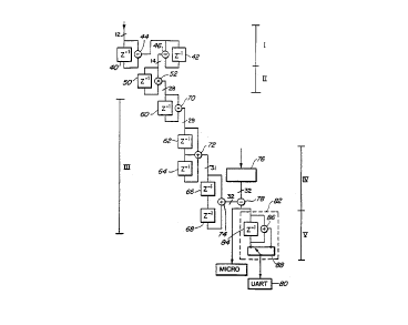
Figure~ 3~shows in~the block diagram a digital FSK
demodulator in a~;:basic~configuration.~ The demodulator is made up
i ~: ' : :
; ~
' ' ~ ; '
WO 93/10611 PCr/CA92/00320
roughly in five stages: high pass filter, quadrature phase detector, low
pass filter, offset generation and sampling doubler
The high pass filter is on stage I and is made up of t~vo unit
delays 40, 42 and su~tractors (negative adders) 44, 46 and will block dc
5 from an input PCM signal and attenuate low frequencies. The input
signal is indicated as a 12 bit signal as an example in this embodiment
and the Figure further shows changes in the bit number of the signal as
it is being processed at later stages. The filter also will eqjualize the side
bands on long telephone loops. The ~llter's frequency response is shown
10 in Figure 4. DC is totally blocked and the attenuation at 60 Hz is -60 dB
with respect to the Nyquist frequency. The attenuation at the lower
sideband is -14.3 dB and the attenuation at the upper sideband is -2.3 dB.
Therefore, the higher sideband is~attenuated by -12 dB with respect to the
lower sideband.~ This will compensate for the sideband distortion on
15 long loops. The~output of the high-pass filter is shown in Figure 5.
The quadrature phase~ detector is well suited for FSK
dete~ion and is provided at stage~ Il. The sampling frequency represents
the reference to which~ the~ two FSK frequencies are compared. The
phase shift relative~ to one quarter of the sampling frequency is detected.
20 The quadrature is a~ process ~by which the~ signal is multiplied by a
delayed version~of itself and ~therefore includes a unit delay 50 and a
multiplier 52. The; delay is~of utmost importance and therefore the
sampling frequency~must not~be changed. DC and low frequency inputs
into the quadrature~will~generate ~frequencies close to the signal
frequency at its output and are therefore hard to remove. DC and low
freq-çn~ties must therefore~be~blocked; from entering the quadrature
process. The hlgh~pass~filter described above is provided for this
purpose. Figure 6 shows~ the output ~of the quadrature in the frequency
domain. The output signal's energy~is concentrated in the 600 Hz peak.
30 The 600 Hz represent the~altemating~mark~/space sequence at 1200 baud.
For random mark/space~sequences the energy would be distributed
,' :
.~
W~ 93l10611 21 1 1 ~ 7 9 PCr/CA92/00320
J
' between dc and 600 Hz if the rate is 1200 ba-ld. Frequencies above 600 Hz
must therefore be removed.
The low pass filter at stage III functions to remove
frequencies above 600 Hz from the quadxature output and consists of
s three filter sections, each made up of a combination of unit delays 60-68
and adders'70-74. The combined frequency re~,ol~se of all three low pass
filter sections are seen in Figure 7. Filter (1,1) followed by filter (I,I,I)
and filter ~I,O,I) also may be realised by the convolution product
(1,2,3,3,2,1). The pole positions of the combined filter are shown in
10 Figure 8. The pole positions are carefully chosen to produce a zero
~!
t' multiplication filter realization. This is also important to minimize the
hardware requirements. The frequency domain of the low pass filters
output is shown in Figure 9. It should be noted that the higher
frequencies are attenuated. Figure 10 shows the time domain of the low
15 pass filter's output.; The "square wave" is the decoded representation for
the altemiting, mark/space sequence ~at; the output of the low pass filter.
The closer this signal resembles~ a square wave, the better the signal's
quality. This signal has~to be oentr~e sampled and refer~l-ced to an offset
level. The offset~level~cannot be assumed to be zero because the
20 spectrum may contain dc. Sideband equalisation will decrease the dc
contents of the sp~ctrum.
The~ ~offset generation i9 used to compensate the dc
'component and'is shown in~the Figure~by an~offset register 76 which, in
this~embodiment,~sends~a~32 bit offset 1evel~signal to a subtractor 78.
25~ After subtracting the offset Ievel, the sign bit can be fed directly to a
UART (Universal~Asynchronaus Receiver/Transmitter) receiver 80 for
bit s~ynchronization.~
However, at a ~sampling rate of 6800 Hz and a rate of 1200
baud,~ there are ~5.667~samples per bit ~and the fractional part of 0.667 will
30 create~ chitter or jittff~at~the UA~T's input. As a further improvement
therefore, in order~ to reduce the~chitter the sampling frequency may be
doubled at this stage~(stage V shown in a dotted box as an option). The
.:~: :
. .. .. : . ,. ,, ..... ~ .. , . , , .~. , .
:'~
:
WO 93/1061 1 ,~ , 9 PCI /CA92/00320
sampling doubler 82 which may be provided here for this purpose as a
further embodiment may consist of a unit delay 84, an adder 86, and a
selector (an electronic switch) 88. The sampling rate is doubled using
50% zero filling followed by a low-pass filter to eliminate the spectral
s mirror image. Thus the switch 88 operates at twice the sampling
~ frequency to select alternately the sampled data signal and an inter-
,,2 polated signal which is sent to the UART receiver 80 in the proper order.
The actual hardware is re~li7ed by a polyphase filter.
The present invention uses the fractional two's
10 complement representation and sequential processing of the signal.
, Furthermore, by taking advantage of the specific speed requirements of a
modem, the hardware implementation can be further simplified as will
be discussed below.~ Thus, in the fo}lowing embodiment, data samples
are received at 6800 Hz or every 147 ,us. This is more than enough time
~'~ 15 to do all operati~ons~sequentially. This will significantly reduce the
hardware requirements and cost as simple and well proven hardware
elements can be used for the design and production of a chip of the
present invention. As seen below, the hardware implementation can be
re~li7~1 by the use of only simple shift registers, adders and latches and
20 requires the minimum number of multipliers.
Referring ~now~to Figure 11, an embodiment is illustrated
in which stages~l~to V correspond to those of Figure 3. In the Figure,
PSR3, PSR11, PSR27 or PSRn indicates 3-bit, 11-bit, 27-bit and n-bit
parallel shift registers. SRl4,; SR34 ~or SRn depicts 14-bit, 34-bit or n-bit
25 shift registers. ADDI, SUB1 and LATCH1 are a 1-bit adder, 1-bit
su~lraclor and 1-bit latch.~ ~
The 12 bit data ~sample is loaded into the parallel shift
registers PSR3 and PSR11~ of stage I ~high pass filter) which further
includes two shift registers SR14, subtractors SUB1 and a latch LATCH1.
,~ 30 Of 12 bits of the data sample, 11 bits are loaded into PSR11 via path 100,
the least significant blt first and the most significant bit last. The 1-bit
sign bit is loaded into 3 positions of PSR3 via path 102, that is to say, sign
,, : .
W~ 93J10611 2 1 1 1 ~ 7 9 PCT/CA92/00320
' bit 1 is loaded as 111 and 0 sign bit as 000. This is equivalent to dividing
the input by 4 to make space for a possible overrun generated by the
subtraction. The two extra positions correspond to two subtractions
;~ because each subtraction operation may generate one bit overrun. It
s should be noted that PSR3 and PSR11 are in a single 14 bit shift register
in which three positions are set aside for the sign bit. The 14 bit output
of the high pass filter is fed to the quadrature phase detector ~stage II)
which includes SR14 and a multiplier. The multiplier can be any type of
two's complement multipliers including a simple shift and add
10 multiplier. The output of the quadrature detector, i.e. the multiplier, is
in 28 bits and is fed to stage III (low pass filter).
The low pass filter includes PSR7, PSR27,5 SR34,4 ADDl
and 4 LATCHI. The ~irst blt of 28 bit output is the sign bit and it is
loaded into 7 positions of PSR7 through path 104 and the remaining bits
into PSR27 through path 106, from the least significant bit first to the
most significant bit~ ~last. The sequential output of the PSR7 and PSR27i5
therefore the least significant bit of the data bits first, to the most
~' ~ significant bit last, followed by the sign bit~ in the same order.
The~offset generator Is stage IV and has an offset register, a
: ~ 20 subtractor, and a ~latch.~ The offset register is either hardwired or a
re~ister which is under~control~of~a microprocessor by way of path 108, in
the latter case,~ the ~offset ~level can~be readily and, if preferred,
dynamically adjusted. ~ ~mong various ways of determining the offset
leYel, one method;~ which~ can be ~used~ is as follows. In the special
telephone environment, a long continuous signal stream of alternating
mark and~ spaoe~is ~provided; at the be~nnin~ of the "ciass burst". In such
a càse,~the output~of ~the low pass filter can be integrated and averaged
; over time. The~integration of aperiodic signal will produce the dc level
of~the signal's spectrùm. ~ This dc lèvel is~used as reference (the offset
3 0 level) for the remaining signal of the ~"class burst".
The;~stage ~V~is the sampling frequency doubler and is not
essential for the operation of the demodulator of the present invention.
,
-
7 9
The stage V is ~e sampling frequency doubler and is not
essential for the operation of the demodulator of the present invention.
However, as stated earlier it improves the yer~o~ nce by reducing the
,.
chitter or jitter. The sampling doubler includes a shift register, an adder
5 and a switch ( or a selector) 110. The shift register and the adder produce
the sampled data signal and ~e interpolated signal of the two ad~acent
sampled data signals. The switch which is operated at twice the
sampling frequency collects both the sampled data signal and the
interpolated signal. The output of the switch is thus the data signal,
o which is sampled at twice the s~ !in~ frequency. It is then sent to a
UART, which is well known hardware universally used in modems.
The signal sent to the UART is ei~er one or zero which is derived from
the sign bit part of the output of the sampling doubler.
The analysis of quantisation errors and overflow :i-s
5 particularly sunple since the circ~it is not recursive. An addition or
subtraction can produce one bit overrun. Therefore a pre-scaling of one
bit and a register Iength increase of one bit will eliminate overrun and
quantisation noise completely. A ~ tiplication will not produce an
overrun condition.~; Quantisation noise is generated unless the register
20 is long enough to hol~ ~e product.
; High pass~ filter~- 2 additions ~equivalent of subtraction) Quadrature ~ -1 multiplication
Low~pass fi~ter - 5 ~ itions
The ~circuit discussed so far genffates zero overrun and quantisation
2s ~ noise.
As can be seen in this embodiment, the hardware used is
simplej reliab1e ~and has ~well proven~ elements. It is therefore very easy
and economical to fabricate into ICs.
:: :
:
.SUB~ lJTE S~