Note: Descriptions are shown in the official language in which they were submitted.
. , . ~ ~~ Express Mail
#RB458514045
WATER TREATMENT SYSTEM BULB STATUS MONITOR CIRCUIT
BACKGROUND OF THE INVENTION
The present invention relates to water~treatment systems,
and more particularly, to a circuit for monitoring the status of an
ultraviolet bulb in such a system.
Household water treatment systems are gaining popularity
-- particularly in areas with less than ideal potable water. A
household unit is mounted on a single tap to treat selectively
water flowing through the tap. Treatment may include filtration,
irradiation, or both.
The most effective water treatment systems include
ultraviolet (UV) irradiation for sterilising the water stream. It
is well known that such UV treatment kills bacteria and viruses
with an extremely high degree of reliability. The water to be
treated is routed through a chamber, and a UV light source within
or adjacent to the chamber directs UV light through the water
stream.
The effectiveness of irradiation depends upon the status
of the W bulb. The bulb may not be operating properly for a
variety of reasons. The bulb may be "burned out"; the bulb may be
broken; or power to the. bulb may be interrupted. Alerting the
consumer to a nonoperative bulb is desirable for two reasons.
First, the consumer is not getting UV-treated water. Since the
water will not look or taste different, the consumer needs to be
alerted. Second, if the bulb is broken, glass shards may be in the
system. In this case, the bulb also could be trying to light,
causing the starter to prematurely fail and/or the ballast to
overheat.
A variety of prior art techniques have been developed for
monitoring bulb status. A first technique includes positioning a
photo detector within the irradiation field to monitor for light
emitted from the bulb. However, such detectors are relatively
expensive, undesirably increasing the cost of the treatment unit.
Examples of this technique can be found in U. S. Patents 4, 769,131;
4,752,401; 4,682,084; 4,665,627; 4,255,383; 3,948,772; 3,491,234;
3,471,693; 3,182,193; and 2,263,162.
A second technique is to provide an indicator, such as a
light-emitting device (LED), that is illuminated when current is
flowing through the bulb and unilluminated otherwise. One
disadvantage of this technique is that the indicator is illuminated
at any time that current is flowing through the circuit regardless
of whether the bulb is illuminated. For example, the indicator
light would indicate proper operation when the bulb is attempting
to light and/or when the circuit is shorted. In neither case is
the bulb actually providing irradiation. Consequently, this
technique provides a false level of assurance. Examples of this
technique are illustrated in U. S. Patents 5,023,460 ; 4,255,663;
and 4,141,686. Another illustration of current monitoring, but
without an LED, is shown in U. S. Patent 4,615,799.
Bulb intensity control circuits may monitor one or more
of lamp output, temperature, voltage, or current. However, the
monitored parameters in such systems are used to control bulb
- 2 -
CA 02111620 2000-10-16
intensity only. Such circuits do not provide any indication of
the bulb status . Examples of such control systems are illustrated
in U.S. Patents 4,831,564; 4,471,225; 4,400,270; and 4,336,223.
SUGARY OF THE INVENTION
The aforementioned problems are solved in the present
invention, which effectively, simply, and inexpensively monitors
the status of the W bulb within a water treatment system. More
particularly, the monitoring circuit includes a voltage detection
circuit coupled in parallel across the bulb. The monitoring
circuit further includes means for emitting a status signal when
the voltage is undesirably high (as might be associated with a
burned out bulb or a broken bulb) or when the voltage is
undesirably low (as might be associated with a short circuit).
More particularly the invention in one aspect pertains
to an improved water treatment system comprising a chamber, an
ultraviolet (W) light bulb for directing W light through the
chamber, a ballast and a starter circuit both connected to the
bulb, and monitor means for monitoring the status of the UV bulb.
The improvement comprises the monitor means comprising, voltage
monitor means for monitoring the voltage across the bulb, and
signal means responsive to the voltage monitor means for emitting
respective signals in response to the monitored voltage being
within a desired range, in response to the monitored voltage
being higher than the desired range, and in response to the
monitored voltage being lower than the desired range.
In another aspect the invention comprehends an
electrical circuit for an ultraviolet (UV) water treatment system
comprising, a W light bulb, a ballast electrically connected in
series with the bulb, a starter circuit electrically connected
in parallel with the bulb, and a first monitoring circuit
connected in parallel across the bulb, the first monitoring
circuit emitting a signal when the voltage across the bulb
exceeds a predetermined high voltage. A second monitoring
circuit is connected in parallel across the bulb, the second
- 3 -
CA 02111620 2000-10-16
monitoring circuit emitting a signal when the voltage across the
bulb falls below a predetermined low voltage, and each of the
first and second monitoring circuits including an opto-isolator
circuit to electrically isolate the monitoring functions from the
W bulb.
Preferably, the status of the bulb is indicated via
status signals that are in a format compatible with a CMOS
(complimentary metal-oxide semiconductor) processor or logic
inputs. Such an arrangement enables the bulb status to be
processed by a microprocessor which would then indicate to the
consumer the status of the bulb in a user-friendly manner.
In the preferred embodiment, the voltage detector is
a pair of circuits, each including a zener diode and an
opto-isolator to electrically insulate the monitoring circuit
from the bulb power circuit. This arrangement is desirable in an
electrical system used in conjunction with water.
These and other aspects, advantages, and features of
the invention will be more readily understood and appreciated by
- 3A -
~~~~r
reference to the detailed description of the preferred embodiment
and the drawings.
BRIEF DESCRIPTION OF THE DRAWINGS
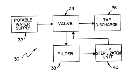
Fig. 1 is a block diagram of a water treatment system in
which the W bulb status monitor circuit of the present invention
may be used;
Fig. 2 is a schematic circuit diagram of a conventional,
and therefore prior art, W power circuit;
Fig. 3 is a schematic circuit diagram of the bulb status
monitor circuit of a first embodiment of the present invention; and
Fig. 4 is a schematic circuit diagram of the bulb status
monitor circuit of a second embodiment o!: the present invention.
DETAILED DESCRIPTION OF THE PREFERRED EMBODIMENTS
The first embodiment of the ultraviolet (UV) monitor
circuit of the present invention is illustrated in Fig. 3 and
generally designated 10. The circuit includes a transformer 12, a
rectification circuit 14, and a signal generation circuit 16. The
transformer 12 is coupled in parallel with a W bulb 20 to step
down the voltage across the bulb. The transformer secondary
current is rectified by the circuit 14 and applied to the circuit
16. A signal is outputted in CMOS compatible form by the circuit
16 whenever the voltage across the bulb 20 is undesirably high or
undesirably low.
The voltage which the bulb 20 inherently seeks is
referred to as "the sustaining voltage." The sustaining voltage
typically is selected to be approximately one-half of the line
- 4 -
CA 02111620 2000-10-16
voltage. Two conditions can drastically change the sustaining
voltage. First, when there is no current through the bulb, there is
no voltage drop across the inductor 52; and the voltage across the
bulb is full line voltage. Second, if the starter shorts out, the
voltage across the bulb is zero.
Therefore, the bulb status can be monitored by detecting
for these three distinctly different voltage levels (i.e. line
voltage, sustaining voltage, and zero voltage) across the bulb.
Sustaining voltage indicates that the lamp is functioning properly.
Line voltage indicates that the bulb is burned out, broken, or
missing. Zero voltage indicates that the starter is shorted out or
that power is interrupted.
The bulb status monitor circuit of the present invention
would be included in a water treatment system of the type
illustrated in Fig. 1 and generally designated 30. The line
connections illustrated between the blocks of Fig. 1 are fluid
connections permitting water flow through the treatment system.
Generally speaking, the water treatment system is connected to a
potable water supply 32 and includes a valve 34 for selectively
routing water either directly to the tap discharge 36 or to the
filter and sterilization units 38 and 40 respectively. The valve
may be of the type illustrated in copending Canadian Application
File No. 2,107,398, filed September 30, 1993, and entitled FAUCET
DIVERTER VALVE.
In the water treatment system 30, the water can be sent
directly to the tap discharge 36 by putting the valve 34 in a first
- 5 -
manually selected position. Alternatively, the valve 34 can be
placed in a second manually selected position where the water is
routed sequentially through the filter 38 and the sterilization
unit 40 before being discharged from the tap at 36. The filter 38
is preferably a carbon-activated filter. The W sterilization unit
includes a water chamber, container, or passageway in conjunction
with an ultraviolet (LIV) source of light for sterilizing water
flowing therethrough.
A conventional W power system for such a water treatment
system is illustrated in Fig. 2 and generally designated 50. The
system includes a W bulb 20, a ballast 52, and a starter circuit
54. The plug 51 or other power connection is conventional and is
selected to be compatible with the power distribution system to
which the circuit is to be connected. Although the power
connection is illustrated as a conventional plug, the system also
may be hard-wired to the power source. The ballast 52 also is
conventional. The impedance of the ballast is selected to reduce
the current through the W bulb to an ideal value for which the
bulb is designed. The bulb 20 is a conventional gas-discharge W
bulb including a pair of filaments 22a and 22b. The filaments are
connected in series with the ballast 14. The bulb acts as a
voltage regulator. As the impedance of t:he ballast increases, the
current through the bulb decreases. Any increase in current
decreases the impedance of the bulb, thus maintaining the voltage
across the bulb essentially constant. Finally, the starter circuit
- 6 -
54 is also of conventional construction and is connected in series
between the filaments 22.
In Figs. 3 and 4, illustrating the alternative
embodiments of the present invention, the components of Fig. 2
other than the bulb 20 have been omitted for clarity. Accordingly,
Figs. 3 and 4 each show the bulb 20 in conjunction only with the
bulb status monitor circuit.
As previously mentioned, the embodiment 10 illustrated in
Fig. 3 includes a transformer 12, a rectifier circuit 14, and a
signal emitting or generation circuit 16. The transformer 12
includes a primary 62 connected in para:11e1 across the bulb 20.
The secondary 64 of the transformer 12 i.s center-tap grounded at
66. The transformer 12 therefore steps down the voltage across the
bulb 20.
The rectification circuit 14 is conventional and includes
a pair of diodes 68a and 68b electrically connected to opposite
sides of the secondary 64. The outputs of the diodes are connected
in series with a resistor 70 having grounded capacitors 72 and 74
on either side thereof. Accordingly, a DC voltage appears at node
76, which is directly proportional to the AC voltage across the
bulb 20.
The signal generation circuit 16 generates a CMOS-
compatible logic output at node 80, which can be used by a
microcontroller (not shown) operating the system. Node 76 is
connected through a zener diode 82, a node 83, and a capacitor 84
to ground. The conducting voltage of they zener diode is selected
_-
so that the voltage generated by the rectification circuit 14 will
not cause the diode to conduct when the bulb is at normal
sustaining voltage. In this embodiment, that voltage is 4.7 volts.
Node 76 is also connected through resistor 86 and diode 88 to the
supply voltage VCC. A battery 98 back-up is connected through
diode 96. Transistor 90 is series connected with resistor 92
between VCC and ground. The output of the transistor 90 at node 80
is the CMOS LOGIC OUT A point. Transistor 94 switches transistor
90 and therefore LOGIC OUT B under the control of the signal at
node 83.
When the primary of the transformer 12 (i..e. bulb
voltage) goes to the line voltage (e.g. 100 volts) (meaning the
bulb is not lit or is trying to light), the zener diode 82 turns
on. The signal at 83 turns on transistors 94 and 90 to provide a
high logic output at LOGIC OUT A and low logic output at LOGIC OUT
B. When the primary voltage of the transformer 12 goes to zero
volts (meaning shorted starter or no power), current will be
supplied to the circuit 16 by the battery 98 back-up as diode 96
will be allowed to conduct because of the absence of the rectified
supply voltage. In such case, both LOGIC OUT A and LOGIC OUT B are
low. When the bulb is at sustaining voltage (e. g. 45 volts)
(meaning bulb lit), the logic output at LOGIC OUT A is low; and the
logic output at LOGIC OUT B is high.
Hence, the output at LOGIC OUT A is high if the voltage
is abnormally high; and the output at LOGIC OUT B is low if the
voltage is either abnormally low or abnormally high. As explained
_ g _
2~I~6~(~
above, abnormally low voltage would indicate no power or a shorted
starter. Abnormally high voltage would mean a burned out bulb, a
broken bulb, or a missing bulb. In any of these events, the
consumer should be notified. On the other hand, the logic output
at LOGIC OUT A is low and the logic output at LOGIC OUT B is high
when the bulb is irradiating.
Second Embodiment
An alternative embodiment of the bulb status monitor
circuit, and presently the preferred embodiment, is illustrated in
Fig. 4 and generally designated 110. The circuit 110 includes a
high voltage monitor 110a and a low voltage monitor ilOb. Monitor
110a emits a high logic output (or in the absence of capacitor 142
a series of pulses) when the voltage is abnormally high, and
monitor 110b emits a low logic output (or in the absence of
capacitor 172 a series of pulses) when the voltage is abnormally
low.
The high-voltage monitor circuit 110a includes series-
connected diode 120, resistors 122 and :124, and zener diode 126
coupled in parallel across the bulb 120. Opto-isolator 130
includes an LED (light emitting diode) or other light-emitting
device 132 and a phototransistor 134. The LED 132 is coupled in
parallel with the resistor 124. A pair of resistors 136 and 138
are series connected between the supply voltage VCC and ground.
The collector of the transistor 134 is electrically connected to
node 140 between resistors 136 and 138. Node 140 is the logic
output. Capacitor 142 is provided between the node 140 and ground
_ g _
for the purpose of filtering out the 60 hertz component of the AC
power signal.
The turn-on voltage of the zener diode 126 is selected as
a value approximately midway between the sustaining voltage and the
abnormally high voltage to be monitored for. In the disclosed
embodiment, this is 75 volts. So long as the bulb voltage does not
exceed this abnormally high voltage, zener diode 126 does not
conduct; LED 132 is not illuminated; transistor 134 does not
conduct; and the logic output at 140 is high. The output at LOGIC
OUT A is high (or in the absence of capacitor 142 a series of
pulses) if and only if the bulb voltage .is abnormally high.
The low-voltage monitor 110d includes series-connected
diode 150, resistors 152 and 154, and zener diode 156 coupled in
parallel with the bulb 20. Opto-isolator 160 includes an LED 162
or other light emitting device and phototransistor 164. The LED
162 is connected in parallel with the resistor 154. Resistors 166
and 168 are series connected between the supply voltage VCC and
ground. Output node 170 is located between the two resistors 166
and 168. Capacitor 172 is included to filter out the 60 hertz
component of the AC power signal.
The logic output at node 170 depends on the voltage
across the bulb 20. Specifically, the conducting voltage of the
zener diode 156 is selected to be between zero and the sustaining
voltage. In the preferred embodiment this is 1.6 volts. When the
bulb is operating at a normal voltage (i.e. sustaining voltage),
the zener diode 156 conducts; the LED 162 is illuminated; the
- 10 -
p,, ~,
phototransistor 164 conducts; and a low logic output is provided at
LOGIC OUT B. When the voltage becomes abnormally low, zener diode
156 does not conduct; and the logic output at node 170 is high.
Accordingly, the output signal at the output node 170 is low (or in
the absence of capacitor 172 a series of pulses) if and only if the
bulb voltage is above the predetermined abnormally low voltage and
high otherwise.
A microprocessor (not shown) i.s coupled to output node
140 and 170 to provide communication with the consumer. The
microprocessor receives a CMOS-compatible signal from the circuits
110a and 110b.
The above descriptions are those of preferred embodiments
of the invention. Various alterations and changes can be made
without departing from the spirit and broader aspects of the
invention as set forth in the appended claims, which are to be
interpreted in accordance with the principles of patent law
including the doctrine of equivalents.
- 11 -