Note: Descriptions are shown in the official language in which they were submitted.
wOg3/007~ PCT/US92/~969
9 ~ :
TITLE
CONNECTOR BLOCK ASSEMBLY
S BAC~GROUND OF THE INVENTION
Field of the Invention
This in~ention relates to wire con~ecting arrangements
and more particularly it concerns novel connector block
assemblies for connecting clo~ely spaced wires on which
high density voice or data information i~ being
conducted.
Descri~tion of the Related Art
There i~ a need in the telecommunications industry to
transmit large volumes of voice or data i~formation
along groups of lines that~are closely spaced from each
other. Moreover, in order to maintain flexibility a~
equipment is added or replaced in a telecommNnications
~y~ten, it is important to ha~e connection ~tatio~s at
one or a few locations where connecti~n~ to a large
number of pleces of equipment ca~ be Nade. This ra1ses
ce~tain problems because i~ order to carry large
~olumes of information over electrical lines, the
information must be transmitted at high frequency and
WOg3/007~ PCT/US92/~ ~9
~ b9~ 2 -
this gi~e~i rise to radiation and interference between
adjacent lines, particularly where the lines are
closely spaced from each other. The radiation and
resulting n cross-talk n can be minimized by t'ransmitting
the information over twisted wires or over wires that
are encased in a conductive sheath. However, when the
wires are brought to a connection station, the
connectors cannot practically be twisted or encased in
a conductive sheath; and because they are close to each
other their i9 a tendency for cross-talk.
The problem of cross-talk is not particularly severe at
low frequencies, for example, less than about 16
megahertz (Mhz); however there is a demand for
transmission at much higher frequencies, :n the
neighborhood of 100 Mhz and at those frequencies,
radiation i~ higher and there is a need~for greater
attenuation between adjacent conductors.
There is also a need for a connector block assembly
that i~i compact and that can handle a very large number
of connection~ in a small ~pace. At the same time the
connector assembly must provide easy access and must be
$ail safe.
~25
Vnited States Patents No. 4,741,711, No. 4,533,196 and
No. 4,283,103 sho* prior art~co: ector assemblies of
t~e type toiwhich the present invention is applicable.
~ach of these patents shows connector block assemblies
in which a plurality of spring finger contact elements
~ are located. However, none of them address the problem
- ~ of cross~talk between~adjacent connector elements or
group~ of con~ector elements.~ Also, none of the prior
art arrangement~ ~hows a ~pring fînger grounding
arrangement which is engaged by~an insert module prior
; to engagement with signal conducting contacts. In
addition, the prior art does not disclose a reliable
W093/~725 PCT/USs2/04969
h 9 l
yet simple means for holding an inser~ module at
different operating positions in a connector a~sembly.
SUMM~RY OF TXE INVENTION
5 , ~
The present invention provides improvements to
connector block assemblies which enable ~he handling of
a large number of connections of wires in a small space
in a convenient manner and with a minimum of cross~tal~
even at high freguency transmi~sion.
According to one aspect of the present in~ention t:here
is provided a novel connector a~sembly for providing a
plurality of closely spaced connections ~o wires which
conduct high frequency electrical signals. This
connector assembly compriRes an elongated insulative
block, a plurality of connector eleme~ts mounted in
closely spaced arrangement within the block a~d a
plurality of electrica~ly conductive shields. The
block is formed with openings which pro~ide access for
individual wires to be connected to the ends of
corre~ponding ones of the connector elements; and the
electrically conducti~e hields are mounted wi~hin the
block between adjacent co~ne~tor elements to prevent
cro~talk between the connector elements.
According to another aspect of the in~en~ion there is
provided a no~el connector block assembly which
c~mprises an insulative block, a pair of electrically
conductive ~ignal contacts and a ground contact mounted
in the block. The signal contacts each haYe a spring
finger biased to contact the spxing finger of ~he other
contact. The block is fonmed with a~ opening pro~iding
acce~ to a probe which can be inserted into the block
to engage and separate the ~pring finger~. The ground
co~tact i~ mounted between the opening and the spring
finger~ to be contacted by the probe when it is
W093/0072S PCT/US92/~969
.
in~erted into the block and before it engages the
spring fingers.
According to a further aspect of the invention there is
pro~ided a novel connector block assembly which
comprises an insulative block, a pair of electrically
conductive signal contacts mounted in said block and an
insert module. The signal contacts each having a
spring finger biased to contact the spring finger of
the other contact. The block is also formed with an
opening providing access to the spring fingers. The
insert module has a projecting insert element which
fits through the opening in the block and engages and
separates the spring fingers; and it also has a module
casing which holds the projecting insert element. The
block and the casing are configured such that each has
a surface which slides along a corresponding surface of
the other as the module is in~erted into and withdrawn
from the block. One surface i8 formed with a detent
and the other is fonmed with a projection which fits
into the detent to hold the insert module in fixed
position relative to the spring fingers.
BRIEF DESCRIPTION OF THE DRAWINGS
- ~ ~
Fig. 1 is a top view of a multiple wire connector block
as~embly which comprises one embodiment of the present
' lnvention,
Fig. 2 is~an exploded top view of the connector block
a~ embly of Fig. 1, showing a base and a contact holder
s-parated from each other with the ba~e and contact
holder portions partiially cut away,
Fig. 3 is an enlarged sectional view taken along lines
3-3 of Fig. 2;
W093/007~ PCT/USg2/04969
9 1
Fig. 4 is a fragmentary perspecti~e view showing the
mounting arrangement for an isolation shield in the
connector block aYsembly of Figs. 1-3;
Fig. 5 is a view taken along line 5-5 of Fig 3;
Fig. 6 is a view taken along line 6-6 of Fig 3;
Fig. 7 is a fragmentary perspective view ~howing the
~0 mounting arrangements for connector elements and ground
elements in the connector block assembly of Figs. 1-3;
Fig. 8 is a view taken along line 8-8 of Fig. 3;
lS Fig. 9 is a view taken along line 9-9 of Fig. 3;
Fig. 10 is a top view, partially broken away, of a
ground element used in the connector block assembly of
P'igB . 1- 3;
Fig. 11 is a side elevational view of the ground
element of Fig. 10;
,
:
Fig.~12~ is an elevational view~ o one side of a-~, ,, 25 protector module used with the~connector assembly of
~Figs.;1-3;';
~: : ~ : :
'' ' ~ Fig.' 13 is~an elevational view of the other side of the protector module,~of~Fig.~12;
:- Fig 14~ i~B -a ~iew~taken~along line 14-14 of Fig. 1 and
showiog~a protector~module~partially in~erted,into the
~" connector assembly;
Fig. 15 is a viéw similar to Fig. 14, but showing the
protector module at a first operating position in the
'' , connector a~sembly;
: :
: :
W093/0072~ PCT/US92/~969
~ 9 1 - 6 -
Fig 16 is a view similar to Fig. 15, but showing the
protector module at a second operating position in the
connector assembly; and
Fig. 17 is a view similar to Fig. 16, but taken at a
different cross-sectional location along the length of
the connector assembly of Fig. 1.
DETAILED DESCRIPTION OF THE PREFERRED EM3ODIMæNT
The connector assembly of Figs. 1-3 is used to connect
pair~ of wires (not shown) from individual telephone
trunks to a central station. However, identical or
similar connector assemblies may be used for
interconnection of other e~uipment, for example, voice
or data lines in a computer netwQrk.
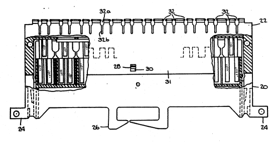
As shown in Figs. 1-3, the connector assembly comprises
an elongated base 20 and an elongated contact holder
22, each molded of plastic material in a ge~erally
block-like form. The base 20 is formed with mounting
tabs 24 at each end, and a cable harness 26 along one
side As can be seen in the cutaway portions of Fig.
1, and aR will be described more fully hereinafter, the
base 20 i~ formed with internal cavities in which
connector, ground and shield elements are mounted. The
contact holder 22 fits onto the base 20 and i8 gnap
locked onto the base by mean~ of projections 28 along
the upper surface of the base. These pro~ections
extend into recesses or openings 30 in a skirt portion
31 of the contact holder which fits over a mating part
of the ba~e 20.
A~ can al80 be ~een in the cutaway portions of Fig. 1,
and as will be described in detail hereinafter, the
contact holder 20 is also formed with internal cavities
into which the connector, ground and shield elements
W093/00725 PCT~US~2/04969
~11i169~
-- 7
extend. One side of the contact holder 22 i8 formed
with slots 32 into which wires to be connected are
inserted. The slots 32 each have first wider portion
32a for guiding a wire into a second narrower portion
32b. The width of the narrower portion 32b is chosen
to be less than the overall diameter of an insulated
wire to be connected, but greater than the diameter of
the conductor portion of the wire. This allows the
wires to be held tightly in the slot~ without imposing
any strain on their conductor portions.
As shown in Fig. 2, the base 20 has a shoulder 34 along
one side and again~t which an edge 36 of the skirt
portion 31 of the contact holder abuts in assembly.
The projections 28 are formed near the shoulder 34 at
~paced apart locations along the length of the base 20.
Similar projection~ and reces~es are pro~ided along the
botton surfaces of the base 20 and the contact holder
22.
The base 20 i8 also formed with recesses 38 separated
by walls 40 for accom~odating pairs of connectors and
ground elements~ A180, pairs of fingers 42 extend out
from the base 20 on~each~side- of each of the recesses
38 for holding connectors in place in the contact
holder 22. Electrically conductiYe shield plates 44
extend~between the ecesses 38~and are~held in slots 46
ro~ided in the walls 40.
~: ~
- 30 The contact holder 22 has mounted therein, in 810t and
~,
cavity arrangement~described~more fully hereinafter,
an electrically conductive ground strip 48 from which
qpring finger ground ele~ent~ SO extend, as well as
pair~ of electrically conductive, spring finger
connector elements 52.
WO93/00725 PCI/US92/04969
2 ~ 9 1 ;` `~
The exploded section view of Fig. 3 i8 taken through a
plane in the body 20 which pa~3es through the slot 46
in one of the walls 40. As can be seen, when the
contact holder 22 is assembled onto the ~ody Z0, the
5 apring finger connector elements 52 and the spring
finger ground elements 50 pass behind the shield 44 in
the body 20. The contact holder 22, as shown in Fig.
3, i8 formed with outer recesses 54 distributed along
the length of the holder near the top and bottom
10 thereof and into which wire attachment ends 56 of the
connector elements 52 extend. As can be seen in Fig.
3, the~e outer reces~es 54 are formed between outer
walls 58 and associated inner walls 60. The outer
walls 58 continue beyond the recesses 54 to form the
15 ~kirt portions 31. Separate recesses 54 are provided
for each of the connector elements 52, which are
distributed in groupa of opposing pairs with the ~pring
finger end~ of the elements of each pair extending from
oppo~ite sides of the contact holder 22 to contact each
20 other along the center llne of the holder. The inner
walls 60 extend continuously-along the length of the
contact holder 22 and~ form between them an elongated
ground~strip channel 62. The ground strip 48 is
mounted in the grou;nd strip channel 62.
The wire attachment~:end 5~6 of each of the connector.
elements 52 is bent into-a U-:shaped configuration and
fita ~nugly into an associatèd connector element recess
~ 54. T~e other.end of ~each connector element 52 i8 a
-~ : 30 ~pring.;finger:~end.:~q~he spring~finger~ end extends
.~- beyond ~its a~-ociated inner wa}l 58 and i8 bent
:~ inwardly to form~a contact 64 which normally abuts a
,
corre~ponding contact 64 on the apring finger end: of a
ma~ing connector element 52. The connector elements 52
35 are re~ilient and the mating contacts 64 of each pair
of elements are re~iliently biased into contact with
each other. Preferably the connector elements are
W093/0072~ PCT/US92/04969
r3 1
stamped out of sheet metal which is resilient and which
has high electrical conducti~ity, for example, temperèd
pre-plated brass.
The ground strip 48, which extends along the ground
strip channel 62, is formed with a generally U-shaped
cross-section, comprising an elongated base 66 as well
as the spring finger ground elements 50 and shield
contact elements 68 which are interspersed with each
other and which extend up from along the opposite edges
of the base. The ground elements 50 are arranged in
pairs and are bent in toward the center of the ground
strip channel 62 ~o that the ground elements of each
pair normally contact each other as shown in Fig. 3.
'5 However, because these elements are resilient they can
be flexed away from each other by insertion of an
insert member between them. The ~hield contact
element~ 68 extend flat against the inner surfaces of
the inner walls 60.
The base 66 of the ground strip 48 rests against a side
wall 70 of the contact holder 22. The side wall 70
extends between the upper and lower inner wall~ 60
along the length of the contact holder.
The s~de wall 70 i~ formed with an elongated ridge 74
along the longitudinal centerline thereof and on the
~ide facing the base 20. Insert slots 76 extend
thrsugh the ridge 74 of the side wall 70 and are
di~tributed therealong to allow the insertion of insert
members, for examp1e protector modules, whi~h when
inserted, extend between and ~eparate the mating ground
elements 50 of the ground strip 48 and the mating
contact~ 64 of the connector elements 52. As will be
explained more fully hereinafter, the base 66 of the
ground ~trip 48 is formed with openings to fit around
the 810ts 74.
W093/00725 PCT/USg2/~969
~1116!3~ /
- 10 -
As can be seen in Fig. 3, each shield plate 44, which
is a thin sheet of electrically conductive material,
for example copper, is shaped to extend over both the
wire attachment ends 56 and the spring finge~ ends,
including the mating contacts 64 of the spring finger
connector elements 52. As shown in Figs. 3 and 4,
these shield plates 44 ha~e an expansive main portion
78 which is inserted into one of the slots 46 in the
walls 40 of the base 20, and two projecting arms 80
which extend into the contact holder 22 in the
assembly. The main portion 78 covers the mating
contacts 64 of the connector elements 52 and the
projecting arms cover the wire attachment ends 56.
It should be noted that in the exploded views of Figs.
2 and 3, the shield plates 44 are shown mounted in the
base 20. This is merely to provide clarity in showing
the structure of the device. Actually, it is
preferable to assemble the device by first positioning
the shield plates 80 that their projecting anms 80 fit
appropriate ~lots fonmed in the contact holder 22.
Then, when the contact holder is fitted onto the base
20 the main portions 78 of the shield plates 44 enter
into the slots 46 in the walls 40 of the base.
As shown in Figs. 4, 5 and 6, wire holders 82 are
fonmed along the top of the base 20. Wire~ (not shown)
to be connected in the device pas3 up through the cable
harness 26 (Fig. 1) and fan out to the various wire
holders 81 before entering through the slot~ 32 in the
contact holder 22.
A180, as ~hown in Fig. 5, each of the recesses 38 in
the ba~e 20 i8 di~ided into four recesses 38a, 38b, 38c
and 38d by means of a pair of walls 82a and 82b which
extend parallel to and midway between each of the walls
40. The rece~ses 38a and 38b form a first pair and
WO 93/0072~ PCI`/US92/04g69
3 ~.
- 11 -
accommodate spring connector elements 52 for a pair of
input wires (e.g. tip and ring wires from an outside
plant in a telephone system) and the recesses 38c and
38d form a second pair and acco~ranodate sprin,~_connec.tor
5 elements for a pair of output wires (e.g. tip an.d ring
wire~ for a telephone subscriber line). The walls 82a.
and 82b leave a space 84 between them to allow
insertion of a probe element which is inserted into the
device via the insert. slots 76 (Fig. 3).
- -
Figs. 5 and 6 also show additional cable harnesses 86
at opposite ends of the ba~e 26.
Turning now to Fig. 7, it will be seen that the
15 recesses 54 in the contact holder 22 are formed by
walls 88 which extend between each outer side wall 58
and its associated inner wall 60. Alao, grooves 90 are,
fonned in the inside surfaces of the outer walls 58 and
the associated skirt portion 31 of the contact holder
20 to acclmodate and~guide the shieId plates 44 along
their opposite side edges. Slots 92 extend into
`; alternate ones of the walls 88 as continuations of the
grooves 90~. :
25 l~e slot 32 in~ the,contact ~holder 22 are arranged to
be each centra11y located with respect to an associated
one of the reces~es~54-~ In addition, the U-shaped wire
attacl~ment~lends 56 of the connector elements 52 are
, ~ each formed with a:~corresponding wire connection slot
' 30 94, wi,th a:wider~entry portion 94a and a narrower
8econd-poreion; 94b.~ When the wire attac}~ment ends 56
of the comlector :elements ~52 are in~e:rted into the
reces~e~ 54 of~the contact~holder 22,~ the wire
co~nection ~lot8 94 of the connector elements 52 become
35 aligned with the wire insertion s1c)ts 32 in the contact
~: holder 22. The wire connection slots 94 of the
connector element~ are narrower than the wire insertion
WQ93/0072S PCT/USg2/04g69
~ 1 6 9 1 ! - 12 -
slots 32 in the contact holder 22. Thus, as a wire is
pre~ised down into one of the slots 94, the sides of the
slot first cut through the wire insulation and then the
sides of the narrow second portion 94b of the slot bite
into and form a positive electrical contact with the
conductor portion of the wire. At the same time the
narrow portion of the wire in~ertion slot 32 securely
holds the insulator portion of the wire without
straining the conductor portion of the wire.
As can be seen in Fig. 8, each of the insert slots 76
in the side wall 70 is aligned with two sets of mating
contacts 64 of associated spring connector elements 52
and one set of ground elements 52 from the ground strip
48. Also, as shown, the wire insertion slots 32 in the
contact holder 22 and their as~ociated wire connection
slots 94 are aligned with the mating contact~ 64.
Thu8, it will be seen that when a wire is laid into one
of the slot a~hlies 32, 94 at the top of the device
and-another wire i8 laid into the aligned slot assembly
32, 94 at t~e bottom of the device, the wires will be
electrically connected to each other via the mating
contact~ 64 which are seen and are accessible through
the associated in~iert slot 76~ The connection between
these wires will be broken when the contacts 64 are
~eparated as by inserting an insulative~member into the
slot 76. ~ ~ ~
,~, , I i
The actual spring coDnector elements 52 with their
contact~elementis can be~seen at~the left end of Fig. 9.
Fig~. 9 al~o shows the ground elements 0 connected to
~- the gr~ound-strip 48,~ as-well as~ground connector
fingers 96 at the end of the ground strip. The
connector fingers are connected~to ground via an
external connection (not shown).
W093/0072~ PCT/USg2/04g69
~1116!~1
-- 13 -
Figs. 10 and 11 show the construction of the ground
strip 48. Preferably this element is stamped out of
sheet metal which is resilient and which has high
electrical conductivity, for example, tempered'pre--
plated brass. The base portion 66 of the ground stripcomprises two spaced apart parallel elongated base
elements 66a and 66b which are bent along their facing
edges to form flanges 66c and which are connected to
each other by bridging portions 66d extending between
the upper edges of the flanges 66c at spaced apart
locations. Between the bridging portions 66, which
extend across the ridge 76 at the same locations as the
walls 40 in the base 20, are openings 98 which are in '
alignment with the slots 76 in the side wall 70 of the
contact holder 22. The ground elements 50 are bent up
from the outer edge~ of the base elements 66a and 66b
at locations midway between the bridging portions 66c,
i.e. in the center of the openings 98. Between the
- adjacent ground elements 50 are the shield contact
elements 68. These~elements are bent up to extend at a
right angle to the base elements 66a and 66b. The
' ~hield contact elements 68 are each split central}y
with lots 100 which divide each~element into two
egmpnts 68a and~68b. The slots 100, which are located
. 2~ in alignment with~the bridging~portions 66c,
acconmodaté the~edge~ of the~shiel'd plates 44 and make,
electrical contact~wit~h~those~plates in~assembly. The
ground connection fingers 96 are bent from the ends of'
the base~elements~66c~and 66b~in generally the same
direction~as the~shield contact elements.
;'~-; ~ Figs.~12 and 13~show opposite;sides of an insert module
102 that can be used in the above described connector
a~ embly. The in~ert module 102 comprises a module
Casing 104 which contains electrical circuits and
related elements ~uitable to the purpose of the module,
~; for example circuit testing, circuit p otection or
WO 93/00725 ` ,. . PCl`/USg2/04969
.. ....
9 1 . . '
- 14 -
circuit access. A blade-like insert element 106
extends out from the module casing 104. The insert
element is shaped to fit into the insert slots 76 and
to enter into the assembly so as to contact~and
s separate the pairs of mating contacts 64 and ground
elements 50 which are aligned with the particular slot
74 in which the element 106 is inserted. The insert
element 106 i8 electrically non-conductive but it has
electrically conductive plating 106a along its opposite
sides to contact the various contac~s 64 and ground
elements 50 when they become separated by the insertion
of the insert element 106. The plating 106a is
electrically connected to the various electrical
circuits and elements contained in the module casing.
The particular arrangement of the plating 106a and of
the electrical circuits and elements within the casing
104 is not part of this invention nor does it relate to
the best mode for carrying out the in~ention. The
specific arrangement of circuits and other elements
will be dictated by the application or use to which the
connector as~embly and the in3ert module 102 are put.
Also such insert modules per se are well known.
Accordlngly, in the interest of clarity, the details of
a particular insert module are not given herein.
As can be ~een from the above description, the spring
f'inger grouDd elements 50 are arranged in line with the
spring finger ends of the spring finger connector
elements 52 80 that an insert element which is inserted
. into ~ne of the slots 76 will first engage and spread
apart the ground elements S0 and thereafter, as it is
~n~erted further, will engage and~spread apart the
contacts 64 of the connector elements 52. The spring
finger connector elements 52 are connected to signal
carrying wires which are inserted into the slot
a~emblies 32, 94 and therefore the spring finger
W093/00725 PCT/US92/W969
6 ~ .~
- 15 -
connector elements 52 and their associated contacts 64
may be referred to as signal contacts. It will also be
noted that one contact of each mating pair of these
signal contacts 52 is arranged along one line_on one
side of a center line in the a~sembly and the other
contact of each mating pair is arranged along a second
line on the other ~ide of the center line. Also, the
probe insert openings 74 are arranged along the center
line. In addition, the signal contacts 5~ extend
within the assembly from their wire connecting ends 52
on one side of the openings 74, around the ground strip
48 to locations on the other side of the ope~ings. The
wire connecting recess assemblies 32, 94 are close to
but are separated from the ground strip 48.
Figs. 14-17 8how different stages of insertion of an
in8ert module into one of the insert slot8 74 of the
connector assembly.
As shown in Fig. 14, the tip of the insert element 106
enters through the ~lot 74 and first contacts the
ground elements 50 and separates them. This is a
particularly advantageous feature of the invention
becau8e it en8ure8 th,at the ground contacts will be
engaged~before any contacts that may be ~carrying a
voltage.-, Thus,, the likelihood of bIowing out circuits
in the lnsert module 102,~is` minimized.
A~ ~hown in Figs. 14 and 15, the casing 104 of the
insert module 102 is formed with a plug portion 108
w~ich'fits snugly between the inner walls 60 of the
,~ contact-holder 22. In addition, the ca8ing 104 of the
in8ert module 102 i8 formed with an~aDm 110 which
extend~ parallel to and spaced from the plug portion
108. The spacing between the plug portion 108 and the '
aDm 110 i~ such that they can straddle one of the outer
W093/00725 PCT/US92/04969
'. ,?
21 ~ ~6~ 16
side walls 58 and an associated inner wall 60 of the
contact holder 22.
A projection 112 i8 formed on an outer surface near the
end of the outer side wall 58 which is engaged by the
insert module arm 110. The arm 110 itself i~ formed
with a pair of detents 114a and 114b, each of which can
accommodate the projection 112. When the insert module
102 is inserted to a first operating position as shown
in Fig. 15, it is held in that position by the
cooperation of the projection 112 and the first detent
114a. In this operating position the insert element
116 has engaged and separated the contacts 64 of the
~pring connector elements. However, the insert module
102 may be pushed in even farther to a second opérating
po~ition, as shown in Fig. 16 where the projection 112
engages the second detent 114b. The projection and
detent thus hold the module steady in this second
operating position.
The ~wo operating positions of the insert module bring
different plated regions 106a of the insert element 106
into~and out,of engagement with the contacts 64 and the
;; ground~elements~50. Thus, different circuit
, ,, 25 eonnection~are~made~possible by~-pro~iding detent and
'' , projection~arrangements which;~hold the~insert module
102 in différent operating position~.~ Also,~the detent
a'nd projection arrangement in cooperation with the plug
an,d arm configuration~provides a ~otable and reliable
~perating structure.
Turning now to Fig.~17,~ which i- the ~ame as Fig. 16
but taken at a different cross-sect~ion along the
a ~embly, it will be seen that the electrically
conducti~e ~hield plates~44 extend~o~er~the area
occupied by the mutually facing surfaces of different
, group of spring connector elements 52. As expIained
:: :
W093/oo7~ " PCT/US92/04969
- ' ~ 9 3,
- 17 -
above, the shield plates 44 are connected to ground by
virtue of their engagement in the slots 100 in the
shield contact elements 68 of the ground strip 48.
These shield plates are capable of preventin~ cross-
radiation between adjacent groups of connector elementsand thus permit very close spacing between these
groups. Accordingly, a high density of signal carrying
wires and connectors is made possible without
undesirable cross-talk.
As seen from the above, the electrically conductive
shield plates 44 have a surface area at least as great
as the projected area between adjacent pairs of the
connector element~ 52.
~",~ ,,," .",, ,,, ~