Note: Descriptions are shown in the official language in which they were submitted.
- 1 - 21~
Information Recording and Reproduclng
Apparatus for Recording and Reproducing
Information by Using a Probe Electrode
BACKGROUND OF THE INVENTION
Field of the Invention
The present invention relates to an information
recording and reproducing apparatus for perfol ~ ng at
least one of recording and reproducing of information,
which uses a principle of a sc~nn~ ng tunneling
microscope or a sC~nnl n~ interatomic force microscope.
Related ~ackaround Art
Recently, a 9c~nn~ng t~lnnel ing microscope
(herelnafter referred to as STM) capable of directly
observing an electron structure of a surface atom of a
con~l-ctor, and an interatomic force microscope which
applles the technology of the STM have been developed
and various applications thereof have been pLoposed.
Part~cul~rly, applications for a recording apparatus
whlch writes information into a ,eco ding medium at a
high resolution and a lep,od~c1 ng apparatus for re~ng
the informatlon written in the recording medium at a
high resolutlon have been developed. In an apparatus
which applies the STM, it has been proposed to
manufacture components thereof by a ~nown technology
called micL. ah~n1C~ or micromach1n~ng (see, for
example, K.E. Pe~e-~en, Proc. IEEE, 70, 420 (1982)).
' ~
,. : .. . .
,, "
~ - 2 - ,
2~ 70
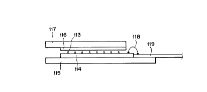
An example is described below.
As shown in Fig. 1, a probe board 114 for
supporting a plurality of probe electrodes 113 and a
lead wire board 119 are provided on a probe base board
115, and the probe electrodes 113 and the lead wire
board 119 are electrically connected with respect to
the respective probe electrodes 113 by co~necting wires
118 such as wire hond~ng. On the other hand, a
recording medium 116 supported by a recording medium
plate 117 is arranged to face the plane of the probe -
plate 114 on which the probe electrodes are provided.
A pulsive voltage for writing a record bit on the
L aao dlng medium 116 by a recording/reproducing voltage
application circult (not shown) is applied between the
leco~ding medium 116 and each of the probe electrodes
113, and a read voltage for reAd1ng the written
information is applied to ~eco,d and ap-oduce the ~ ~-
lnformation.
Ilc~_v~" in the aonven~lonal recordlng and
~ep,od~cing apparatus described above, the probe plate
and the L eco,ding medium are in a very close position
ln the recordlng and reproduc1ng modes. As a result,
ess the electrlc lead wires from the probe plate are
optimally ~esigned, the conneoting wires which are
.~o~e~ing parts wlth the lead wire plate lnterfere
wlth the ~eCG~ ding medium plate or the recordlng
medium, 80 that there will arlse a problem that the
" ' '' ~ ; ,' ~ "
. , ,, ~, . . ' .: ~ .~ .
2111770
connecting wire~ are shorted each other or the
connecting wires are broken. This problem is serious
particularly when the probe electrodes and the
recording medium are relatively moved in a plane by a
large distance.
SUMMARY OF THE INVENTION
It is an object of the present invention to
provide an information recording and reproducing
apparatus which optimize the wiring of the lead wires
from the probe plate ~o prevent the interference with
the recording medium and the recordlng medium plate
when the recording medium and the probe electrodes are
relatively moved.
The above ob~ect i8 aohieved by an information
recording and ,ep-od~cing apparatus, which is provided
with probe electrodes supported by a probe plate and
arranged to face a recording medium supported by a
recolding medium plate, moving means for relatively
moving the recording medium and the probe electrodes,
voltage appllcation means for applying a voltage
between the recording medium and the probe electrodes,
and electric wire take-out portion for taking out
electric wires provlded on at least one of a plane of
the probe base plane oppostte to the probe ele~-odes
and a plane of the recording medlum plate opposite to
the recording medium.
'" ' :
- CA 02111770 1998-04-20
-
-- 4
In the information recording and reproducing
apparatus of the present invention, since the electric
wire lead means for taking out the electric wires is
provided on at least one of the plane of the probe
plate opposite to the probe electrodes and the plane of
the recording medium plate opposite to the recording
medium, the electric wires are taken out of the plane
opposite to the plane to which the probe electrodes and
the recording medium face. As a result, there is no
projecting member other than the probe electrodes
between the probe plate and the recording medium, and
even if the probe electrodes and the recording medium
are relatively moved in the plane, the electric wires
do not interfere with the recording medium or the probe
electrodes.
BRIEF DESCRIPTION OF THE DRAWINGS
Fig. 1 shows a sectional view of a neighborhood of
a probe plate and a recording medium for illustrating a
positional relationship between the probe plate and the
recording medium in a conventional information
recording and reproducing apparatus,
Fig. 2 shows a block diagram of one embodiment of
the information recording and reproducing apparatus of
the present invention,
Fig. 3 shows a sectional view of a neighborhood of
a cantilever of the probe plate shown in Fig. 2
- CA 02111770 1998-04-20
Fig. 4 shows a sectional view of a neighborhood of
the probe plate and the recording medium for
illustrating a positional relation between the probe
plate and the recording medium shown in Fig. 2
Fig. 5 shows a perspective view of a probe plate
and an electric circuit board shown in Fig. 4,
Fig. 6 shows a sectional view of a neighborhood of
a cantilever of a probe plate in other embodiment of
the information recording and reproducing apparatus of
the present invention, and
Fig. 7 shows a sectional view of the recording
medium shown in Fig. 4.
DETAILED DESCRIPTION OF THE PREFERRED EMBODIMENTS
An embodiment of the present invention is now
explained with reference to the drawings.
Fig. 2 shows a block diagram of one embodiment of
the information recording and reproducing apparatus of
the present invention. As shown in Fig. 2, conductive
probe electrodes 1 are fixed to free ends of
cantilevers 2 made of elastic material. The fixed ends
of the cantilevers 2 are fixed to a probe plate 3 made
of a silicon single crystal substrate. An xy drive
element 6 including a piezo-electric element has one
end thereof fixed to the probe plate 3 and the other
end thereof fixed to an inslde of a main body 7, so
that the probe electrodes 1 can be driven in xy
2~11770
directions by the xy drive element 6. Accordingly, the
probe electrodes 1 can be moved to any position in the
xy direction.
On the other hand, a recording medium 8 includ~s a
record layer having a Squarilium-Bis-6-n-Oatylazulene
(SOAZ~ dye organic thin film deposited on a gold
electrode, and the gold electrode of the recording
medium 8 is formed on a medium plate 80. A z drive
element 9 including a piezo-electric element has one
end thereof fixed to the medium substrate 80 and the
other end fixed to the inside of the main body 7, so
that the medium plate 80 is driven in the z direction
by the z drlve element 9 and the recording medlum 8 is
moved ln the z direction. As seen from the above
descrlption, the drive means for relatively moving the
probe electrodes 1 and the recording medium 8 ls
constituted by the xy drive element 6 and the z drive
~1 e, 1, 9.
A probe position controller 10 controls the z
posltion of the probe electrodes 1 (a SpAC~ ng be~leon
the probe electrode 1 and the ,eoo~ding medium 8) and
the xy posltion of the probe electrodes 1 by
lnstructlon of ~tgnal proo~s~ ng, or slgnal from tlming
con~,oller 13 or switching circuit 11, and it is
co~ns~ed to the xy drlve 9~ e ? ~ 6 and the z drive
ql f sr~ 9. The switching circuit ll swltches ~ Al9
to the probe ele~odes 1 by a slgnAl from the timing
cor.~,oller 13, and switches the signal from the probe
.. .
;,
'' '~ '
.,
211177~
electrodes 1 and transmits it to a waveform shaping
circuit 14. A recording/reproducing voltage
application circuit 12 which serves as voltage
application means applies a pulsive voltage to write a
record bit, to the recording medium 8 by a signal from
the timing controller 13, and applies a read voltage to
read the written information. The timing controller 13
is connected to the probe position controller 10, the
switching circuit 11 and the recording/reproducing
voltage application circuit 12 to eontrol the time
division processing of the recorded and reproduced data
and the allocation of the reeord signals to the probe
eleetrodes. The waveform shaping circuit 14 which
serves as current detection means detects a current
flowing between the recording medium 8 and the probe
eleetrodes 1 to reproduce the information recolded by
the signal from the probe electrodes 1.
A structure of the probe plate 3 is explained in
detail with reference to Fig. 3. Fig. 3 shows a
seetional view of a neighbo,l,ood of a eantilever of the
probe plate shown in Fig. 2. As shown in Fig. 3, the
eantilever 2 to which the probe eleetrode 1 iB fixed is
made by depositing a re~ ent oxide ~ilm 20 and an
eleetrieal slgnal wire 40. The probe eleetrode l i8
eleetrleally connected to the eleetrleal slgnal wlre
40. The fixed end of the eantilever 2 is fixed to one
plane of the probe plate 3 made of a s~l~eon single
,
- 8 - 2 ~7 7 0
crystal plate, and an electrical wire lead portion 4 is
formed on the other plane of the probe plate 3. The
electric wire lead portion 4 includes a conductive
member 41, a conductive film 42 having a metal vapor-
deposited thereon, and a le~i ng wire 43 by wirebon~;ng which serves as an electrical wire for taking
out an electrical signal out of the probe plate 3. An
electrical signal from the probe electrode 1 flows to
the electrical signal wire 40, the conductive member
41, the con~uctive film 42 and the lead wire 43
se~uentially, whereby the electrical signal is taken ~ ~;
out to the plane of the probe plate 3 opposite to the
probe electrode 1.
The electric wire lead 4 of the present embodiment
is formed in the followlng manner. Ions are t ~lAnted
to that portion of the silicon single crystal substrate
(probe plate 3) having both sides thereof polished
which i8 to be formed into the conduotlve member 41.
Then, an area from a rear side (an upper plane ln Fig.
3) of the sillcon slngle ~y~al to the lon implanted
portion which ls to be ~ormed into the conductlve
- ~er 41 is eleotrolytlcally etched by potassium
hyd~o~lde (KOH) solution. Thus, the conductlve - ~- 41
18 formed at the bottom of the hole formed by the etching.
Then, chromium (Cr) 18 evapGrated on to the hole
through a mask, and gold (Au) i8 applied to ~orm the
conductive film 42. A bond~ng pad for the wlre hon~1n3
. ~ ,
. ; ' ' ,
,
- - 9
2~ ~177~
is provided on the conductive film 42 as connecting
means.
The probe electrodes 1 and the cantilevers 2 are
formed in the following -nne.r. A thermal oxidization
film is formed on a silicon single crystal substrate to
a thickness of 0.3 ,um, and as many oxide films 20 as
the number of cantilevers 2 to bs formed, which are of
lever shape having a length of 100 ,um and a width of 20
,um, are patterned. A pattern of the electrical signal
wire 40 is then formed on the oxide film 20 and a
predeteL ~ned portion of the silicon single crystal
substrate is etched by potassium hydroxide (KOH) solution
from the upper surface to form the cantilevers 2.
Then, carbon (C) is deposlted to a height of 5 ,um at
the ends of the cantilevers 2 by an eleatron beam
deposition method to form the probe electrodes 1.
A positional relationship between the probe plate
3 and the recording medium 8 (see Fig. 2) is now
expl~1ne~ with reference to Figs. 4 and 5. Fig. 4
8hows a sectional view of a ne~ghborhood of the probe
plate and the recording medium for illustrating the
positional relationship be~.~een the probe plate and the
recording medium shown in Fig. 2, and Fig. 5 shows a
~eI ~pective view of the probe substrate and the
electric circuit board shown in Fig. 4. As shown in
Flg8. 4 and 5, an electrlo clrcult board 5 (which
lncludes the circuits 10-14 of Fig. 2) for effecting
... . .. .. ...... .
~. ..
o 21~7~0
the control is attached to the plane of the probe plate
3 opposite to the probe elec~ode 1, and the lead wires
43 are co~n~cted to the signal wires through a bond~ ng
pad (not shown) formed in the electric wiring area 51
of the electric circuit board 5 from the electric wire
lead 4 formed on the probe plate 3. Electric parts 52 ~
for ~oce~slng the signals from the probe ele~lodes 1 ~ -
are mounted on the electric circuit board 5 and they
are connected to the con~,ol unit through an external
connection unit 53 having a fle~l hl e printed circuit
board. The recording medium 8 is arranged to face the
probe electrodes 1.
In the present construction, only the probe
elec~sodes 1 pro~ect to the plane of the probe plate 3
faclng the recording medium 8. Thus, when the probe ~:
plate 3 and the recordlng medlum 8 are relatively moved
in a plane, the lead wires 43 do not interfere wlth the ;
~eco.ding medium 8. As a result, the degree of f.~ed~
ln arrAnglng the probe substrate 3 and the ~eco-ding
medium 8 is lncreased. Further, since the electric
~n~l wires from the probe elec~odes 1 are co~e~ed I ;
to the electric circuit ln short paths wlthout routing
the probe plate 3, the circuit is resistable to
di~urbance.
Fig. 6 shows a ~ectional view of a ne~ hGrl~ood of
the cantilevers of the probe plate in ano~l.e.
embo~1 sr~ of the lnformatlon ~~co dlng and .ep.~ n~
;. " :'
'~' -11- 2~770
apparatus of the present inventlon. In the present
embo~ nt, the conductive probe electrodes 1 are fixed
to free ends of the cantilevers 2 having a resilient
and conductive film 21 and electrical signal wires 40
and they are electrically connected to the conductive
film 21 and the electrical signAl wires 40. The fixed
ends of the cantilevers 2 are fixed to the probe plate
3 made of a silicon single ~y~al substrate. The
electrical wire lead 4 includes electrlcal signal wires
40, conductive film 21, conductive wires 44 having
metal evaporated thereon, and a metal bump 45 formed to ;
take out the electrlcal slgnals out of the probe plate -~
3. The electrical ~lgnal from the probe ele~L ode 1 -
sequentlally flowes to the conductive film 21, the
electrlcal 8ignal wires 40, the conductive wires 44 and
the bump 45, so that the electrlcal ~lgnal is taken out
of the plane of the probe plate 3 oppo~lte to the probe
ele~odes l. The probe plate 3 and the eleatric ;
clrcult board 5 are electrlcally conne~;led by using
condl~otive partiGles 47 contalned ln an anlsG~o~
oo.-l.cLlve sheet 46 between the bump 45 facing the
probe plate 3 and the ele~L~ode pad 55 facing the
electrlc clrcult board 5. The ~acordlng medlum (not
shown) 18 arranged to face the probe eleo~odes 1. ~
The probe plate 3 of the y~aser~ ment 18 ~-
~ormed in the followlng manner. Ions are lmplanted to
a 811 ~con slngle ~ly~al substrate having both sides
-~ - 12 - 2~ ~77 ~
thereof polished to form a conductive member, and a
plurality of lever shaped conductive films 21 having a
length of 150 ~m and a width of 30 ~m are patterned
(only one lever is shown in Fig. 6). Then, a pattern
of the electrical signal wires 40 is formed and
electrolytic etching is conducted by potassium
hydroxide (KOH) solution to the ion implanted area from
a rear side (upper surface in Fig. 6) of the silicon
single crystal substrate. Thus, the cantilevers 2 and
the levers with short electrical wire leads are formed.
Chromium (Cr) is evaporated to the short levers through
a mask, and gold (Au) is applied to form the conductive
wlres 44. The bumps 45 for the anisotoropy co~uctive
sheet 46 are provlded on the conductive wires 44.
Then, carbon (C) is depos~ted to a height of 5 ,um at
the ends of the cantilevers 2 by an electron beam
flepo~ltlon method to form the probe electrodes l. In
this ?nnsr~ the probe ele~odes 1 are formed at the
ends of the cantilevers 2 on the probe plate 3.
The probe plate 3 and the electric circuit board 5
are csnnected in the ~ollowing -- er. The aniso~oroyy
condllctive sheet 46 having a number of co~ductive
particles 47 uniformly dispeL~ed in the bond is
posl~loned between the probe plate 3 and the electric
alrcuit board 5, and it i8 heated and pressurlzed 80
that the oon~lctive particles 47 are physically
contacted only vertically (between the bump 45 and the
. .
~ - 13 -
2~17~0
electrode pad 55) to make it conductive.
In the present embodiment, like in the embodiment
shown in Fig. 3, only the probe electrodes 1 pro;ect to
the plane of the probe plate 3 opposite to the
~e~olding medium (not shown). Accordingly, when the
probe plate 3 and the recording medium are relatively
moved in the plane, the conductive wires 44 do not
interfere with the recording medium. Further, since
the electrical signal wires 40 from the probe
electrodes 1 can be connected to the electric circuit ~
board 5 in a short path without routing to the probe ~ -
plate 3, the circuit is resistable to disturbance.
In the embodiments described above, the electrical
wires are taken out from the nei~hborhood of the probe
ele~LIodes l to the opposite side of the probe
substrate 3 although the present provided on the probs
plate 3 and the electric wires may be taken out of the
end of the probe plate 3. The position to taken out to
the opposite side of the probe plate 3 is not limited
to that described in the embod~ ~nts. Further, while
the probe plate 3 is described in connection with the I ;
take-out of the electric wires, it may be applied to
the medium plate 80 (Flg. 4).
This is explained in detail with reference to Fig.
7. Numeral 80 denotes a recording medium plate made of
a sllicon ~ingle crystal substrate, numeral 81 denotes
a recording medium underlying electrode having gold
:
'' '~
: ' : '' ,',
.
~ 14 - 2~1770
(Au) epitaxially grown, numeral 82 denotes a record
layer having a Squarilium-~is-6-n-Octylazulene (SOAZ)
dye organic thin film deposlted on the recording medium
underlying substrate by an LB method, nl - al 83
denotes an electric wire take-out portion formed on the
plane of the recording medium plate opposite to the
ecoLd layer, n~ - al 84 denotes a con~uQtive member,
n~ - al 85 denotes a co~ductive film having gold ;;~ ;
e~apo~ated, and nl ~ al 86 denotes an electrical wire
for taking the electrical s1 gn~l out of the eco ding
medium plate 80. Thus, the info ?tion s~gnal from the
Leao~d layer 82 flows to the ~ecor~ing medium
underlylng ele~,ode 8~, the co~uctive member 84, the
oonduGtive fllm 85 and the lead wlre 86 sequentially,
80 that the lnformatlon 81gnA1 may be taken out from
the plane of the recordlng medlum substrate 80 opposite
to the L~UO d layer.
The eleotric wire lead 83 ln the present
embodlment 18 formed in the same manner as that of the
eleotrio wire lead 4 of Fig. 3. It 18 also effective
where the underlylng ele~lode of the ~e~o~ding medium
8 i8 divlded lnto a plurality of portions. The
eleotrioal con~e~ion bet~en the probe plate 3 and the
eleotrloal clrcult board 5 may be made by solds~ing but
preferably it i8 made by solderless mountlng method
suoh as con~uGtlve bond con~e~lon, conductive plated
resin ball co-~ec~ion or dlreot connection by gold bump
- - 15 -
~177~
and insulative resin.
The present invention offers the following
advantages.
Since the electric wire lead for taking out the -
electric wire is provided on at least one of the plane
of the probe plate opposite to the probe electrodes and
the plane of the recording medium plate opposite to the
recording medium, there is no projecting member other
than the probe electrodes between the probe plate and
the recording medium. Thus, when the probe electrodes
and the recording medium are relatively moved in the -~
plane, the electric wires do not interfere with the
recordlng medium or the probe electrodes. As a result,
the recording and reproduclng apparatus having a high ;~
degree of freedom in arranging the probe plate and the
L ecolding medium substrate is attained.
Further, since it is not ~ecess~ry to route the
electric wires on the plate, the length of the electric
wlres can be shortened and the s~gn~l from the probe
ele~odes is resistive to the external disturbance and
the design of the probe plate having a plurality of ~ ;
probe electrodes is facilitated.