Note: Descriptions are shown in the official language in which they were submitted.
WO '~3/OU688 2 I 1 I 8 4 ~ PCI'/GB92/01162
The present invention relates to electrical devices, for exarnple
circuit prot~ction deYices, and to their rnethods of manufacture. :.
In particular, the devices comprise material that has a positive
temperature coefficient of resistance (PTC) and that undergoes a
significant and sharp increase in resistance at a specified
temperature or over a specified narrow temperature range- above
ambient temperature.
PTC materials, which may be polymeric or c~ramic, are known for
use in electrical devices such as heaters, and aiso for protectin~
electrical circuits against excessive curren~ or temperature. The ~ ;~
excessive temperature may itself arise simply from current
flowing throughl the device, or may be due to an increase in the ~:
ambient temperature beyond a desired value. Details of
developmsnts relating to conductive polymer PTC compositions
and devices comprising them, are given for example in U.S. Pat.
Nos. 4,017,715, 4,177,376, 4,246,468, 4,237,441, 4,238,812,
4,329,726, 4,255,698, 4,272,471, 4,445,026, and 4,327,351, and
GB 2,038,549. It has been proposed to use devices comprising
PTC elements to protect circuits against fault conditions arising , ~:
from excessive temperatures and/or circuit currents in for
example U.S. Pat. Nos. 2,978,66~, 3,243,753 and 3,351,882, U.K.
Pat. No. 1,534,715, the article entitled nlnvestigations of Current
Interruption by Metal-filled Epoxy Resin' by Littlewood and :
Briggs in J.~Phys D: Appl. Phys, Vol. Il, pàges 1457-1462, and the
article entitled "The PTC Resistor" by R. F. Blaha in Proceedings
of the Electronic Components Conference, 1971, and the report
entitled "Solid State Bistable Power Switch Study" by H. Shulman
and John Bartko ~August 1968) under Contract NAS-12-647,
published by the National Aeronautics and Space Administration.
U.S. Pat. Nos. 4,238,812 and 4,25~,698, disclose practical circuit
protection devices comprising conductive polymer PTC elements.
:,:
wo 93/nu688 q. k ~ - 2 - Pcr/Gss~/nI l62
The disclosure of each of the patents and publications referred to
above is incorporated herein by this reference.
The present invention is concerned particularly, though not
exclusively, with electrical devices comprising PTC materia~,
preferably polymeric, for use in circuit protection, and US Patent
Nos. 4,238,812 and 4,329,726 referred to above for example,
disclose such devices. PTC circuit protection devices are such
that under normal operating conditions, determined by the current
and temp~rature rating of the PTC material, they exhibit Yery low
resistance to the flow of current therethrough. Under fault
conditions, of excessive current and/or temperature, the PTC
material heats up, significantly increases its resistance and thus
switches off the flow of current therethrough, thereby protecting
an associated electrical circuit. The higher the resistance of the
material after passing through the switching transition, the
lower is the residual current that can flow through the device,
and thus the more effectively is the device in protecting its
circuit. Products embodying these principles are presently sold
by Raychem Corporation under its tradename POLYSWITCH. Some
of such products are formed from a substantially hornogeneous
sheet of polymeric PTC material. The sheet is coated over each `
of its major surfaces with electrically conductive material, to
act as electrodes, anc disc, rectangular, or other, shaped devices
are stamped therefrom.
'
The resistivity of the PTC material of POLYSWITCH devices
typically does not exceed -0 ohm-cm, and taking a typical value
of 5 ohm-cm and a disc configuration with typical dimensions of
diameter 2 cm and thickness 0.05 cm, the resistance at room
temperature (ie. abnut 20 C) of the device is typically 0.08 ohm.
Although other ~eometries, for example rectangular, can be
employed, the resistance values provided by devices that are of a
siz~ that can conveniently be handied manually do not vary ;~ -
significantly from the values given above. If it is desired to
make such devices of different resistance, then this can be
arranged in various ways: (a) a different PTC material having a
w~s3/on6s8 2111~-~4 PCI/GB92/U1162
different resistivity can be employed. However, it has be~n found
that polymeric materials in sheet ferm suitable for circuit
protection devices and having a resistivity greater than about 10
ohm-cm cannot reproducibly be manufactured in si~nificant
volume. This makes it very difficult to produce devices havfng a
significantly higher resistance. This is, of course, not
necessarily true for polymeric PTC rnaterials in general, but has
been found to be so for ma~erials needed for circuit protection
devices in view of their need to have a relatively sharp transition
from low resistance to high resistance as the temperature
increases, for example due to a current increase above a
threshoid value; (b) the separation of the electrodes can be
varied, but for sheet material it is difficult reproducibly to
increase the thickness enough to produce a suitable device having
a significantly higher resistance. The difficulty encountered is
that of provialing, by extrusion for example, a relatively thick
sheet of a polymeric material that is highly loaded, for example
by as much as 50% of its volume, with fillers such as carbon
black, in which the composition of the material is homogeneous
throughout. In this respect, it should be noted that a typical
width of extruded sheet is 30 cm; and (c) The diameter (or other
planar) dimension of the stamped product can be varied. However,
below a certain size it becomes very difficult physically to
handle the individual devices, so again there is a problem with
producing devices of higher resistance. For these practical
reasons therefore it is difficult to make such devices having a ;
resistanc~e greater than say about 5 ohms. However, there is a
requirement for~ higher resistance devices in order to limit
current in electrical~ or electronic circuits to less than about
200mA at normal operating voltages. In this respect, it is to be
noted that the power generated in the device (12R) must be large ~ ~
enough to raise the lemperature of the PTC material up to the ~ -
temperaturfl at which its resistance increases sharply, so that
the lower the current flowing through the device the higher must
be its resistance.
, ~ . .... . ..
2~ PCII~(-B92/0116~
Other POLYSWITCH products produced by Raychem are of s~rip
rather than disc form, but with strip configuration, the short
length of the strip needed for a sufficiently high resistance
device to protect cireuits adequately~àgàinst currents below
about 200mA would be too small ~or eàsy handling.
EP-A-0 087 884 discloses a further polymeric PTC circuit
protection device in which a cylindrical element of PTC material
is mounted within an enclosure between cup-shaped electrodes at
each end thereof. -
We have discovered that convenient PTC circuit protectiondevices, partioularly though not exclusively of polymeric
material, can be made of higher resistance reproducibly using
known sheet F'TC material and applying conductive rraterial (for
formation of electrodes) at selected spaced apar~ locations on
one side of the sheet. Current flow between the electredes is
thus substantially parallel to the major (usually planar) surfaces,
and thus along the length, of the sheet and not directly through
its thickness. A greater range of resistances in devices can thus
be produced from a sheet of material that itself has a given
resistivity and thickness. Such devices can be made of easily
handleable size whilst still having the desired high resistance.
It is one object of the present invention to provide a method of
manufacturing an electrical device, for example a circuit
protection device, whereby devices of different resista`nce can be- i
produced conveniently from the same base material, for example
PTG material, preferably polymericj in sheet form.
It is another object of the present invention to provide a method
in accordance with the said one objeot of the invention, whereby
devices of handleable size produced from shset and having
significantJy higher resistance than those previously known can
be produced.
W(~ 93/00688 2 1 118 ~ ~ PCl'/G~92/01162
It is a further object of the present invention to provide
electrical devices, for example circuit protection devices,
preferably made from polymeric PTC sh~et material. having
higher resistance than kr~own devices. ^-
In accordance with one aspect of the present invention, there is ~ .
provided a mcthod of manufacturing a plurality of electrical
devices, the method comprising:
.. .
(a) producing a substantially homogeneous, and preferablyplanar, shcet of a ma~erial having a positive temperature
coefficient~ (PTC) of resistivity;
(b) locatinq electrically conductive members spaced apart from
each other on the PTC material, preferably on at least one major
surface of the sheet; and
(c) cutting the sheet, in on~ or in two dimensions, thereby to
produce a plurality of electrical devices (which may be
substantially planar) each of which has at least two of said
conductive members thereon that are spaced apart from each
other such that, in use, current flow therebetwaen is
substantially parallel to the major surfaces of the sheet of PTC
material.
By the term "substantia!ly homogeneous sheet of material" is
meant a sheet throughout whose entire volume the composition of
.. . .
the material is substantially homogeneous.
It will be apprèciated that in the region of the conductive
mémbers through ~which, in use, current flows, the direction of
the current will in general not be parallel to the major surfaces
of the sheet, but that elsewhere, ie substantially throughout the
device overall, the direction of current flow will be substantially
parallel to those surfaces. This is in contrast with circuit
protection devices made from PTC sheet material heretofore
available, in which the direction of current flow is perpendicular
:
;
WO 93/00688 ~,, 44 - 6 - PCI/GB92/01162 ~i
to the major surfaces ie. perpendicular to the electrodes of the
devices and through the thickness of the sheet.
It will be also appreciated that although the devices sf the
invention are ~orm~d from a sheet`of material, preferably in a
planar configuration, the deYices themselves either by
manufacture or by use need not be planar.
Preferably, the PTC material comprises polymeric material.
Pre~erably, the sheet is produced by extrusion.
Preferably th~ electrically conductive members are located on ;~
the sheet of PTC material, at suitable locations, before the sheet
is cut to prociuce the plurality of individual electrical devices.
However, it is also envisaged that the PTC sheet may be cut into
individual portions and the electrically conductive members
subsequently appropriately located ~hereon.
The conductive members may be locateci on one only or on both of
the major surfaces of the PTC material. The cutting of the sheet
may r~sult in devices that themselves have conductive members
on one or both of their major surfaces. The conductive members
may be applied in disçrete form to the PTC sheet and may or may
not be themselves cut by the cutting step (c). A conductive ~ `
member may be applied as one or more continuous strips, for
example along an edge of the shéet, and may be cut in step (c) so
as to provide conductive members,~ serving as eleotrodes, for a
plurality of devices. Conductive material may be applied as a
continuous layer, for example by deposition, or a photo-resist
method, to-one or bolh major surfaces of the sheet. Subsequently
part of the layer may be removed from the sheet, for example by
atching, so as to provide a pluraiity of conductive members
thereon. Preferably, a conductive sheet or foil, for example of
0.025 mm thickness, is hot-pressed on to the PTC material.
Alternatively, conductive material may be applied to the sheet of
PTC material by a continuous deposition process. This could
.- . .. .... ; .. ,., ... ~,
2 1.~
~,v~93~00688 - 7 - PCI~/GB92~01162
convenien~ly involve the use of a mask such that discrete
electrod@s are deposited. The deposited laysr could be a film of
thickness about 25 microme~ers, which could be built up, into a
thicker film if necessary, by successive depositions.
The electrical devices formed from a single sheet by the method
of the invention may be generally rectangular or circular, or have
any other required shape. The devices are particularly applicable
for use in circuit protection devices, the conductive members
acting as electrodes.
As set out above, the resultant conductive members of each
device are such that, in use, current flow is substantially parallel
to the major surfaces o~ the device, and it is specifically
required that substantially no current at all flow transversely
thereof (since this wo~Jld give rise to a lower resistance path
that wouid reduce the effectiveness of the dsvice since the
current at which the device would protect an associated circuit
would be higher). However, it may be convenient, or indeed
desirable, for example for the purpose of making electrical ~ ~
connection to the device, actually to have conductive members on ~ ~ f `
the PTC material on opposite faces thereof. It rnust then be
ensured, however, that the electrical connections are such that
substantially no current can flow through the thickness of the
PTC material. This may be achieved, for example, by electrically
interconnecting (short-circuiting) appropriate conductive -
members, or just by allowing them to adopt the local électrical
potential (float) without making any connection thereto.
Advantageously, for high resistance devices, the thickness of the
sheet of PTC material is less than about 2 mm, and may be about `~
1 mm, and preferably is less than about 0.5 mm, whilst its
resistivity is as high as can conveniently and reliably be
achieved, typically being up to about 10 ohm-crn.
Particularly advantageous embodiments of device produced by the
method of the presPnt invention are rectangular in shape, and ~ -
wo s3/00688 ~ 3 4~ - 8 - PCI/GB92/0116
hav~ a rectangular conductive member extending along each of
two opposing edges thereof ~i) both on the same surface, or (ii) on
opposing surfaces of the sheet of RTC material. Typically, such
devices may be of length about 15 rr~m and width from about 2 mm
to 10 mm.
.
In accordance with anoth~r aspect of the pres~nt invention, there
is provided a circuit protection device comprising a substantially
homogeneous sheet that (a) is formed of material having a
positive temperature coefficient of resistance, (b) has a -
thickness less than about 2 mm, (c) has on at least one major ~ ;
surface thereof two electrodes that are spaced apart such that, in
use, current 11ow therebetween is substantially parallel to the
major surfacesi of the sheet, and (d) has a resistance (along the
current flow path between the electrodes) at 20 C that is
greater than 1 ohm.
The electrodes may or may not be on the same major surface ofthe sheet of F'TC material.
Thus, the resistivity of the PTC material, which is preferably
polymeric, the thickness of the sheet, and the size and separation
of the conductive members are selecte~ such that the devices of
the invention have a resistance at room temperature (that i~s to
say at 20 C) of at least 1 ohm, prefera~ly at least 20 ohms, and
typically 100 ohms. Such devices can limit trip current up to
about 400~nA.~ -
Advantageously, the resisthfity of the PTC material is as high aspossible, and in practice is preferably greater than 1 ohm-cm.- -
Preferably the device of said another aspect of the presentinvention is produced by the method of said one aspect of the
present invention. However, it is envisaged that the electrodes of
the device could be applied to the PTC material as discrete
components. In this latter respect, for example, a substrate, such
as a printed circuit board, may be itself provided with electrodes
21118~4 ;
WO 93/00688 9 PCI'~GB92/01162
that are arranged to clamp on to, or otherwise make good ~ ~;eleçtrical contact with, the PTC strip. Thus, the olectrod~s,
although pref0rably being bonded to the PTC material, may simply
be in good physical contact therewith.
Advantag~ously, the method and device of the present invention
are such that the device is provided with means for encouraging
the formation of a local ho~ spot in the PTC material, so that the :~
concantratcd heating will more quickly give rise to tripping of ~:
the device. The hot spot, which may be linear, that is to say a hot
line, should be located away from the electro~es, thus preferably
halfway therebetween, so as to avoid any damage thereto. The .:
hot spot can c:onveniently be.encouraged by locally reducing the
amount of PTC material pr~sent.
In accordance with a still further aspect of the present invention, .. ::
there is provided an electrical circuit comprising at least one
electrical component susceptible to excessive current and/or
temperature, and a device arranged to protect the component
thereagainst, wherein the protection device comprises a
substantially homogeneous sheet of PTC matarial of thickness
iess than 2.0 mm, the sheet being mounted in the circuit with two :
spaced apart electrodes in good ~lect!ical contact therewith such . :~
that, in use, current flow between the electrodes is substantially
parallel to the major surfaces of the PTC sheet and such that the
resistance at 20 C of the PTC material between the electrodes is
greater than 1...ohm.
.
Methods of manufacturing electrical devices, and eiectrical
devices themselves, in accordance with the present invention,
will now be described, by way of example, with reference to the
accompanying drawings, in which: :
Figure 1 shows one embodiment of a PTC sheet with nine
identical devices each as shown in Figure 1A cut therefrom; ~:
Figure 2 to 4 show alternative embodiments of devices;
WO 93/00688 - 1 0 - PCI /GB92/01162 -
Figures 5A, ~B and 5C show three devices having different
configurations for enhancing switching performance; and
Figure 6 shows a plan view of a further~modification of the -~
devic~ of Figure 1A. `~
;., :,
Figure 1 shows a plan view of a rectangular sheet 2 of polymeric
PTC material of 0.5 mm thickness having a resistivi~y of 4 ohm-
cm. Conductive material, nickel, of thickness 1 mil (25 micron)
is deposited on to one surface only of the sheet so as to provide a
relatively narrow strip ~ along each of two opposing edges, and
two relatively wide strips 6 equispaced therebetween. By cutting
the sheet 2 along the symmetrical lines AA', BB', CC', and DD', nine
substantially identical devices are formed, each as shown in
Figure 1 A.
::
If conductiYe material has been deposited in strips on both sides
of the sheet 2 of Figure 1, a device as shown in Figure 2 is
produced, the upper conductive members being referenced A and
the lower B. To avoid current flow from electrodes A to
electrodes 13 directly (ie 4A to 4B, and 6A to 6B) through the
thickness of the PTC material 2, pairs of the electrodes can be
shorted out as shown by the discrete conductors 8. Alternatively,
the pair of B electrodes could be left unconnected. As a further
alternative, the pair of electrodes 4A and 6B (or 4B and 6A) could
be left unconnected. The iattcr arrangement is equivalent
e!e~trically to the device of Figure 3.
Figure 3 shows a further embodiment of device, in which the
conductive mate!ial is deposited in strips on the PTC sheet 2
alternatively on upper and lower major surfaces so that after
cutting, th~ device has one end electrode 4A on an upper surface
and an opposing end electrode 6B on a low~r surface.
~ . ~
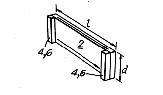
In each of Figures 1A, 2 and 3, the direction of current f!ow
through the device, as shown by the arrow, is substantially
paraiiei to the piane OT the PTC materiai. Taking Figure 1A as an
WO 93/00688 ~ . Pcr/GB92/olt62
example, the separation 8 mm of the electrodes, and their -
transverse dimension 4 mm determines the resis~ance of the
device, for a PTC material of giYen resistivity and formed as a
shcet of given thickness. Thus, simply by varying the disposition
of the conductive matcrial, for example the Icngth and separation
of the strips 4, 6, devices of different resistances can
conveniently be produced. For sxample, a 0.5 rnm thick sheet of
resistivity 4 ohm-cm with d = 4 mm and I = 8 mm, will provide a
device at room temperature having a resistance of about 80 ohms
and a circuit protection current of about 30mA.
Figure 4 shows a device of generally circular configuration that
has been stamped oult of a larger sheet. In this example, a central
disc electrode 10 and an outer annular electrode 12 are disposed
on and separated by PTC sheet material 14.
~ .
Although the invention has been described in r~spect of producing
rectangular or circular configuration devices, each of the same
size, from a single sheet of given resistivity and thickness, it
will be appreciated that by selecting a different configuration of
conductive material, devices having other resistances, and thus ~ ;
other values of circuit protection current, can conveniently be
produced from the same sheet.
Using photo-etching, the separation of the electrodes across the
surface of the PTC material may be as little as 0.1 mm, but
typically the electrode separation would lie in the range from
about 0.2 to 1.0 cm. The thickness of the sheet of PTC material
would typically be from about 0.25 to 1.0 mm.
Figures 5A (plan view~, 5B (plan view) and 5C (perspective view)
show respective ways of enhancing the perfsrmance of the circuit
protection device of Figure 1A. It will be appreciated that in
operating conditions in which the current through, and/or
temperature of, the device becomes excessive thus needing it to
trip to protect its associated circuit, it is desirable that the
tripping, or switching, action takes place as quickly as possible.
WO s3/0o6ss ~ 4 4 - 12 - PCI~/GB92iO116~
This can be enhanced in the case of overcurrent protection if the ~ ~ ;
formation of a local hot spot can be enc~uraged. Each of these
Figures achieves that effect, by providing a region, for formation
of a so-called hot line, of reduced PTC material, thereby locally
enhancing the current density and reducing the thermal mass~
preferentially. This region is concentrated away ~rom the
electrodes, preferably halfway along the device, thus avoiding
damage to the electrodes and also avoiding any heat sink effect
they may otherwise create. Thus, the device 20 of Figure 5A has
holes 22 formed therethrough; the device 24 of Figure 5B has a
pair of notches 26 cut in the sides thereof; and the device 28 of
Figure 5C has a channel 30 in one of its major surfaces.
Referring to Figure 6, the device 32 cornprises a sheet (or strip)
34 of PTC polymeric material of 0.5 mm thickness and resistivity
5 ohm-cm. Three nickel electrodes A, B, C are applied to one
surface thereof such that the separation of A and B is 4 mm and
of B and C is 8 mm. The device 32 can be arranged to have
different current protection values depending on how electrical
contact is made betNeen the electrodes A, E3, C and the associated
electrical circuit. For example, if external conductors are
attached only to the electrodes A and B, the resistance between
these electrodes, 133 ohms, gives a protection current
therebetween of 21mA. In this configuration, electrode C, and the
PTC material Iying between electrodes B and C, is superfluous and
plays no part in operation of the device. Alternatively,
conductors can be attached to eiectrodes B and C, giving a device
with ~ resistance of 266 ohms and a protection current of 18mA.
In a fur~her arrangement, electrodes A and C can be connected
together directly by an external conductor, and conductors taken
from electrodes B and C to an external circuit. This effectively
results in a device formed from two PTC resistors A-B and B-C
connected in parallel, giving a combined resistance of 90 ohms
and a protection current value of 40mA. Clearly, other
combinations can be made.
:;
wos3/00688 13 2111~ 1 PCI/GB92/01162 ~;
In genaral, therefore, it is seen that by using a device having
three, or more, electrodes thereon, and by selecting the spacing
between them, a single device can be used in a variety of ~ -
applications where different protection currents are required.
The devices may be mounted between clips on a circuit board,
when the device of Figure 2 may be particularly suitable, or
terminal conductors may be connected to the conductive members
(electrodes) thereof, for ease of connection into an electrical
circuit.
It will be appreciated that any one device in accordance with the
present invention may have some or all of the features disclosed
in all the described embodiments.
,..:
,
':
`~
...