Note: Descriptions are shown in the official language in which they were submitted.
211~~~J
EhECTRONIC TRIP DEVICE COMPRISING A TEST DEVICE
BACKGROUND OF THE INVENTION
The invention relates to an electronic trip device for a
multipole electrical circuit breaker protecting an electrical
power system, comprising
- a current sensor per pole supplying a secondary current
representative of a current flowing in an associated conductor
of the power system protected by the circuit breaker,
- test current input means,
- a detection and rectifying circuit, to which the secondary
currents and test current are applied, supplying signals
representative of the currents flowing in the conductors to be
protected and of the test current,
- an electronic processing unit receiving the signals supplied
by the detection and rectifying circuit and delivering a
tripping order, with or without a time delay, when the currents
flowing in the conductors to be protected, an earth fault
current or a test current exceed preset thresholds.
Test devices for electronic trip devices generally comprise a
test socket equipped with terminals to which a test current is
applied. This current simulates a fault current which could
occur on secondary windings of the current transformers or
sensors. According to the connection mode of the test socket
terminals, the current is added or combines with the sensor
currents in order to test the whole of the trip device. In
state-of-the-art trip devices comprising protection functions
called thermal or long delay, magnetic or short delay, and earth
fault for earth protection, a discriminator enables the earth
CA 02112029 2004-08-09
2
protection to be tested independently. When the test current is
applied in a first direction, positive polarity on a first
terminal and negative on a second, the trip device does not take
account of this test current for earth protection and trips on
long delay or short delay. If the current direction is inverted
the trip device uses the test current to determine a value
representative of the earth fault current and tripping is
brought about by the earth protection. The means for determining
the value representative of the earth fault current and the
means for discriminating the test current are, in state-of-the
art manner, integrated into the detection and rectifying
circuit, as in French Patent FR-2,592,998, corresponding to the
Patent EP-235,479.
In highly integrated electronic trip devices, the means for
determining the value representative of the earth fault current
are included i.n the processing unit, so as to reduce the cost
and volume of the components. For the same reasons state-of-the-
art type test current discrimination means can no longer be
advantageously incorporated in the rectifying circuit.
SUMMARY OF THE INVENTION
The object of the invention is to achieve an electronic trip
device comprising a test device, with a simplified detection and
rectifying circuit, and integrating means for detecting the
presence of a test current and means for differentiating earth
protection testing in the processing unit.
According to the present invention, there is provided an electronic trip
device for
a multipole electrical circuit breaker protecting an electrical power system
comprising:
- a current sensor per pole supplying a secondary current representative
of a current flowing in an associated conductor of the power system protected
by
the circuit breaker,
CA 02112029 2004-08-09
3
- test current input means,
- a detection and rectifying circuit, to which the secondary currents and
test current are applied, supplying signals representative of the currents
flowing
in the conductors to be protected and of the test current,
- an electronic processing unit receiving the signals supplied by the
detection and rectifying circuit and delivering a tripping order, with or
without a
time delay, when the currents flowing in the conductors to be protected, an
earth
fault current or a test current exceed preset thresholds,
an electronic trip device characterized in that the electronic processing unit
comprises means for detecting a test current of a period greater than that of
the
electrical power system to be protected.
Preferably, according to one embodiment of the invention, the means for
applying the test current are connected to the detection and rectifying
circuit so
as to supply on output of the detection and rectifying circuit at least one
summed
signal representative of the-sum of the test current and of the current
supplied
by one of said sensors or by an earth fault sensor.
According to a preferable embodiment, the processing unit comprises means for
determining the sign of the summed signal or of the test current.
In a preferred embodiment, the processing unit comprises means
for determining the time during which said sign keeps a preset
value, and means for comparing this time with a preset duration.
Preferably, according to the invention, the processing unit comprises means
for
performing an earth protection function and means for inhibiting said earth
protection function.
According to a preferable embodiment, the means for applying the test current
comprise a first terminal, connected to an output of a secondary winding of a
first current sensor and to a first input of the detection and rectifying
circuit, and
CA 02112029 2004-08-09
3a
a second terminal, connected to an output of a secondary winding of a second
current sensor and to a second input of the detection and rectifying circuit.
According to another preferable embodiment, the processing unit comprises
correction means connected between the detection and rectifying circuit, and
circuits for performing tripping functions, said correction means being
connected
to an output of the test current detection means supplying a signal
representative of the presence of a test current.
4
BRIEF DESCRIPTION OF THE DRAWINGS
Other advantages and features will become more clearly apparent
from the following description of illustrative embodiments of
the invention, given as non-restrictive examples only and
represented in the accompanying drawings in which
Figure 1 represents a simplified block diagram of a circuit
breaker in which a trip device comprising the invention can be
implemented.
Figure 2 represents a diagram of a trip device according to an
embodiment of the invention.
Figures 3 and 4 show current signals when a trip device is
tested in operation and out of operation.
Figure 5 represents the architecture of a particular embodiment
of the circuit of a trip device according to figure 2.
Figure 6 represents the flow chart of a processing according to
an embodiment of the invention.
Figures 7 and 8 illustrate the values of the signals when a
differentiated test of the long delay and earth protection is
performed.
DETAILED DESCRIPTION OF THE PREFERRED EMBODIMENT
Figure 1 represents a state-of-the-art circuit breaker. An
electrical power system 1 to be protected is composed of
electrical conductors, generally corresponding to the three
phases and neutral of a system. Contacts 2 enable the current to
be established or interrupted in the phase conductors. In the
figure as in a great many systems, the neutral conductor is
2~.~~~~~
distributed without being broken. Current transformers Tl, T2,
T3 and TN associated with the different conductors of the power
system transform the primary currents of high value into
secondary currents compatible with electronic trip devices. A
test circuit with auxiliary terminals P1 and P2 enables a test
current to be received from a test generator GT to check
operation of the trip device. The secondary currents and test
current are applied to the input of a phase, neutral and earth
fault current rectifying and detection circuit 3. This circuit
supplies signals representative of these currents to an
electronic processing unit 4. A tripping order 20 produced by
the processing unit 4 is applied to the input of a control relay
which actuates an opening mechanism 6 of the circuit breaker
contacts 2.
In the electronic trip device represented, the value of the
earth fault current is determined in the processing unit and the
rectifying and detection circuit 3 does not comprise a component
discriminating between the earth protection test and the long
delay or short delay test, in terms of the direction of the test
current supplied by the generator.
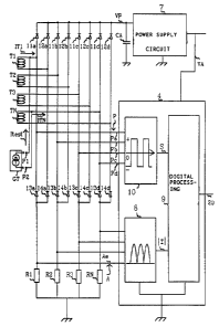
The diagram of a trip device according to an embodiment of the
invention is represented in figure 2. Each secondary winding of
the current transformers is connected to a rectifier bridge
represented by a group of four diodes. For each current
transformer T1, T2, T3, TN, a first end Pa, Pb, Pc, Pd of the
secondary winding is connected to the anode of a first
associated diode lla, b, c, d and to the cathode of a second
associated diode 13a, b, c, d, whereas a second end of the
secondary winding of T1, T2, T3 or TN is connected to the anode
of a third diode 12a, b, c, d and to the cathode of a fourth
associated diode 14a, b, c, d. The cathodes of the first and
third diodes (lla, b, c, d; 12a, b, c, d) are connected to a
positive power supply line vp. The anodes of the second and
211~~~~
6
fourth diodes associated with a secondary winding (13a, 14a;
13b, 14b; 13c, 14c; 13d, 14d) are connected to a first terminal
of an associated measuring resistance (R1, R2, R3, RN), the
other terminal of each of the measuring resistances being
connected to an electrical reference ground of the trip device.
The positive power supply line Vp charges a capacitor CA and
supplies an input voltage to a power supply circuit 7. The
circuit supplies a regulated voltage VA for supply of the trip
device. The first terminals of the resistances R1, R2, R3, RN
are connected by conductors A to the inputs of an amplitude
processing circuit 8. The output of the circuit 8 supplies a
digital processing circuit 9 with rectified signals II~
representative of the absolute values of the currents of the
power system to be protected.
The first end of each current transformer T1, T2, T2, TN is
connected by a conductor Pa, Pb, PC, PD to the input of a
current sign detection circuit 10. This circuit 10 supplies on
an output S, for each input, a first value if the current sign
is positive and a second value if the current sign is negative.
The output S of the circuit is connected to the digital
processing circuit 9.
In this embodiment the test circuit comprises two auxiliary
terminals P1 and P2. The first terminal P1 is connected to the
first end of the transformer T1 also corresponding to the
cathode of the diode 13a, to the anode of the diode lla and to
an input Pa of the sign detection circuit 10. Likewise, the
second terminal P2 is connected to the first end of the
transformer TN, to the cathode of the diode 13d, to the anode of
the diode lld and to another input Pd of the sign detection
circuit. With this type of connection a test current generated
between terminal P2 and terminal P1 is added to the secondary
current of the transformer T1 and is subtracted from the current
of the transformer TN.
2~~~~~~
When a current IT1 of positive polarity is flowing in the
secondary winding of the transformer T1, it flows via the diode
lla to charge the capacitor CA and supply the trip device via
the circuit 7. The current return is via ground and the
measuring resistance R1, then via the diode 14a and the second
end of the transformer secondary winding. The presence of
positive current increases the voltage of the conductor Pa to a
value greater than OV. The sign detection circuit detects this
voltage and supplies on its output a first value representative
of the positive polarity of IT1. The voltage measured at the
terminals of the resistance R1, between a conductor Aa and
ground, has a negative voltage. If the current IT1 is of
negative polarity, the second end of the transformer secondary
winding has a positive voltage. The current flows via the diode
12a to charge CA and supply the trip device, the return flow
being via the measuring resistance R1 and diode 13a. The
measuring voltage R1 between Aa and ground is always negative
whereas the voltage at Pa becomes negative and the sign
detection circuit supplies on output a second value,
representative of the negative polarity of IT1. The currents
flowing in the other secondary windings of the current
transformers (TN, T2, T3) and directed by the associated
rectifying diodes produce the same effects on the sign detection
circuit 10 and the inputs of the amplitude processing circuit 8.
The assembly, comprising the current transformer T1, diodes lla,
12a, 13a and 14a, resistance R1, connections Pa and Aa, and the
parts of the circuits 8, 9, 10 corresponding to the current IT1,
form a channel for measuring the current of a first phase.
Figure 3 shows a representation of the currents and signs when a
test is performed. The current IT1 is the sum of the current of
the secondary winding of the transformer T1 and of the test
current. ITN represents the current of the secondary winding of
the transformer TN from which the test current is subtracted.
2112D~~
8
Indicators SI1 and SIN represent the signs respectively of IT1
and ITN. They can for example take a positive value VP if the
current is positive and a negative value VN if the current is
negative or zero. The test current represented in figure 3a is
zero between the times t0 and tl, positive, flowing in the
direction P2 to P1 in the test signal generator GT between the
times tl and t2, and negative, flowing in the direction P1 to P2
in the generator between the times t2 and t3. The alternating
currents ITl and ITn are respectively represented in figures 3b
and 3d. They supply between t0 and tl sign signals respectively
SI1 and SIN (figures 3c and 3e) whose values change at each
half-wave. When a positive test current Itest, of a value
greater than the amplitude of the secondary winding currents, is
applied between the times tl and t2, IT1 remains of positive
polarity and ITN of negative polarity in continuous manner, and
the sign signals SI1 and SIN keep fixed values respectively VP
and VN. If the test current is inverted between the times t2 and
t3, IT1 is of negative polarity and SI1 is equal to VN and ITN
is of positive polarity, and SIN is equal to VP.
The same type of test can be carried out on a circuit breaker
not in operation. In figure 4, the currents of the secondary
windings of the transformers T1, 2, 3, N are zero, IT1 (figure
4b) is equal to the test current and ITN (figure 4d) corresponds
to the inverted test current. The sign signals SI1 (figure 4c)
and SIN (figure 4e) respectively represent the polarity of ITl,
i.e. Itest, and ITN, i.e. inverted Itest.
According to this embodiment, detection of the presence of a
test current can be performed by means enabling the permanence
of a sign on one of the inputs of the processing circuit
corresponding to one of the measuring channels receiving the
test current to be determined. The value of this permanent sign
signal makes it possible to differentiate the test by enabling
earth protection testing for a first value of the sign signal,
2112,0~~
9
and disabling it for a second value corresponding to a different
sign. Although two sign signals SIN and SI1 are available, only
one is in practice used to implement the invention. In the
description which follows, the sign SIN will be used for the
purposes of test detection.
The architecture of an embodiment of the processing circuit 9 is
represented in figure 5. Sampling circuits 11 and 12
respectively sample the signals representative of the rectified
currents 'I' and the signals representative of the signs S of
said currents. The samples of the current values Ie and signs Se
are applied to the input of a circuit 13 for determining the
value of the earth fault current IT.
Tn this embodiment the circuit 13 computes the value of the
current IT by performing the vector sum of the values of the
currents flowing in the conductors to be protected. 'rhe values
of the samples ~ Ie ~ whose corresponding sign Se is of positive
value are added, and the values of the samples whose
corresponding sign Se is of negative value are subtracted. The
current value samples ~Iel and the value of the earth protection
current can be applied to the inputs of a circuit 15 for
computing the rms values, respectively IRMS and ITRMS. The
values of the rms currents IRMS representing the current
transformer currents can be corrected by a correction circuit 16
before being applied to circuits 18, 19 respectively performing
Long delay LR and short delay CR tripping functions. The value
of the earth protection current IT or ITRMS is applied to a
circuit 17 performing an earth protection function PT. The
circuits performing the LR, CR, PT protection functions supply,
in state-of-the-art manner, a tripping signal 20 when preset
current and time delay thresholds are exceeded.
According to this embodiment, the sign signals Se or S are
applied to a circuit 14 for determining test current presence.
211~U~~
lU
The circuit 14 detects the presence of a test current when a
sign signal, for example SIN, has a constant value for a time
t(SIN) greater than a preset time tmin, itself greater than the
period of the electrical power system to be protected. When the
circuit 14 has detected the presence of a test signal, it
determines the sign of the test current so as to determine
whether the test involves the earth protection function or the
other tripping functions. If the test current presence
information indicates that the sign of SIN has a value Vp for a
time greater than tmin, it is the other tripping functions that
are being tested. The circuit 14 then supplies an inhibition
signal 22 to the circuit 17 performing the earth protection
function PT. In this way, the current signals applied to the
circuits 17, 18, 19 will only be taken into account by the
tripping circuits other than the circuit 17.
In the case where an earth protection function test is involved,
it is not indispensable to inhibit the other functions as the
earth protection function threshold and time delay are generally
lower than those of the other functions. When the presence of a
test current is detected by the circuit 14, a signal 23 can be
applied by the circuit 14 to the correction circuit 16, so as to
enable the tripping threshold and time correction parameters to
be modified.
The processing circuit 9 can comprise a microprocessor
programmed in such a way as to perform the functions of the
circuit represented in figure 5. An example of a flow chart is
illustrated in figure 6. In a stage 24, measurement of the
currents and reading of the signs is performed for processing of
the tripping functions. Detection of the permanence of a sign
and differentiation of the type of test are performed in a
module 25. A comparison stage 26 detects whether the value of
the sign SIN is equal to the value VP. If this equality is true,
a counter Cpt is incremented (Cpt = Cpt + 1), in a stage 26a, if
21~.N~2~
11
not this counter is zero reset in a stage 26b. Processing of the
LR, CR, PT tripping functions is performed in a stage 27 and
checking inhibition of the earth protection tripping function is
performed by a module 28. This module comprises a tripping
request detection stage 29, a tripping request differentiation
stage 30, an inhibition checking stage 31 and a stage 32
producing a tripping order. When at stage 29 a tripping request
is detected, stage 30 differentiates this request. If the
request does not correspond to an earth fault trip, a tripping
order is directly produced by stage 32. In the case of an earth
protection tripping request, stage 31 checks inhibition by
comparing the value of the counter Cpt with a preset threshold
value Scpt. A value of Cpt greater than Scpt corresponds to
permanence of the value of the sign signal SIN at the value Vp
and to the presence of a test current with inhibition of the
earth protection which avoids the tripping stage 32. A value of
Cpt lower than Scpt is representative of operation without test
current or with an earth protection function test current.
Figures 7 and 8 illustrate the different signals as a function
of time. At a time t10 (figure 7a), a positive current Itest is
applied to the test terminals. The absolute value of this
current ~II (figure 7b) is greater than preset long delay or
short delay tripping thresholds 33 and than a preset earth
protection function tripping threshold 34. The value of the
neutral channel sign SIN is blocked at a value VP (figure 7c)
and the value of the counter Cpt (figure 7d) starts to increase.
At the time tll, the counter threshol d Scpt is exceeded and an
inhibition signal 35 takes a value 36 (figure 7e). When the test
current was applied at time t10, the protection functions
started their time delays. A signal TPT representative of the
earth fault protection time delay or temperature rise (figure
7f ) exceeds a tripping request threshold 37 at a time t12
subsequent to tll. However tripping will not take place, as the
value 36 of the inhibition signal 35 disables the effects of the
12
earth protection tripping request. A signal TLR representative
of the long delay function time delay or temperature rise
(figure 7g) reaches a tripping request threshold 38 at a time
t13. The tripping signal 20 (figure 7h) takes the tripping
validation value 39 and orders opening of the circuit breaker.
If a negative test current is applied at the time t20 (figure
8a), the absolute value ~I) of this current is greater than the
tripping thresholds 33 for long delay and short delay and 34 for
earth protection (figure 8b). The value of the sign SIN is
blocked at a value VN (figure 8c) and the counter value remains
at a value lower than the threshold Scpt (figure 8d) . The
inhibition signal 35 is not activated (figure 8e). The earth
protection time delay signal TPT (figure 8f) increases then
exceeds the tripping request threshold 37 at the time t21. As
the inhibition signal 35 is not active, tripping is possible and
the signal 20 takes the value 39 to order opening of the circuit
breaker (figure 8h). The long delay function time delay signal
TLR (figure 8g) reaches the tripping request threshold 38 at the
time t22 after the earth protection function tripping time t21.
In the embodiment in figure 6, detection of the presence of a
test current is performed by a counter Cpt which is incremented
or zero reset. To reduce sensitivity to certain disturbances,
the variations can be performed by a slow increase and a fast
decrease of the counter value.
In the embodiment described above, detection of the permanence
and value of the sign is performed on the neutral current
measuring channel, but any other channel could be used. The test
terminals P1 and P2 are respectively connected to two first ends
of two sensors respectively T1 and TN, however the test
generator can be connected to other ends and other sensors. In
other embodiments the test terminals P1 and P2 can be connected
directly to additional components of the rectifying circuit and
13 2~.~.2~2~
comprise rectifiers specific to the test channel. The test
current is then applied directly to the circuits 8 and 10. The
invention can be applied to other types of circuit breakers,
notably those which comprise current transformers or sensors,
for the neutral or earth protection, outside the circuit breaker
case. If an external sensor is on the neutral line, the
secondary winding is connected to the internal detection and
rectifying circuit 3 and operation is identical to that
described above. In the case where an external earth fault
current sensor has its secondary connected to the detection and
rectifying circuit, the invention applies in the same way. The
test current is then added to the earth fault current
transformer current and means will make it possible to detect
the presence of a test current and to differentiate according to
the direction of the current whether the test is intended for
the earth protection function. The value of the earth fault
current is read directly on the earth channel via the detection
and rectifying circuit and is not determined according to the
absolute values of the phase currents and their signs. However,
as in the previous embodiments, a sign signal will serve the
purpose of test current detection.