Note: Descriptions are shown in the official language in which they were submitted.
.-~ 2ll2nfi2
TECHNICAL FIELD ~;~
The present invention relates to communication
protocols and particularly to a technique for effectively
communicating messages to electronic labels for the latter ~ ;~
to display information in an electronic price display
system.
~ACKGROUND OF THE INVENTION
Much attentlon has been given in recent years to
systems used in retail stores for displaying prices of
goods. While manual marking of the prices at the location
of the goods, or on the goods themselves, is conventional,
attempts have been maqe to use electronic means, instead,
for displaying the prices at the goods location.
2i~2n~2
A28919-1586/21879
Some electronic pricing systems have been proposed
to employ electronic labels or modules, each typically
having a liquid crystal display, for displaying the prices.
Buses for power and data are used in such systems to connect
many thousands of such labels to a central computer for the
latter to communicate with particular ones of the labels to,
for example, request changes in their displayed prices. To
this end, the labels are equipped with connectors so that
they can be snapped onto one of many locations along rails
which include the buses, and which run along the edges of
store shelves. The connectors also provide the labels with
electrical connections to the central computer through the
buses.
In order to provide customers with helpful
15 information such as brand names of the goods other than ~
their prices, it is desirable to have an electronic label ~-
capable of displaying a string of characters, which may be
too long to cover in one display screen and need to be
divided into several screens. It is also desirable to have ~-
20 a broad selection of characters for display to achieve an !~
effective conveyance of the information. It is undesirable
however that while the string of characters for display is
being updated, the label displays incomprehensible informa-
tion. Accordingly, in order to coordinate the display
function of individual labeIs well, it is important for the
central computer to communicate effectively to them.
`` 2 1 ~
~ A28919-1586/21879
~ .
SUMMARY OF THE INVENTION
In accordance with the invention, communication
from the central computer to labels is accomplished by
sending messages addressed to the individual labels. The
labels each comprise a screen having individually actuable
character elements, combinations of which define different
display characters, and at least one memory for storing data
bits contained in the messages addressed thereto. In
accordance with an aspect of the invention, each one of the
character elements is associated with a different stored
data bit in the memory. To display information on the
screen, a subset of the character elements are turned on,
namely, the ones which are associated with the stored data
bits having a predetermined value.
In accordance with another aspect of the inven-
' tion, each label includes a plurality of memories, each of
which contains display data. A second message communicated
from the central computer to a label contains pointer data
which selects one of the memories in that label. A subset
~ 20 of the character elements on the label screen are turned on
i in response to the display data stored in the memory thus
selected.
In accordance with still another aspect of the
invention, each memory comprises a plurality of memory ele-
ments for storing display data. The memory elements arecyclically read in a certain order to display, on the label
screen, information based on the display data stored there-
in. A thlrd message communicated from the central computer
to a label contains an indicator. Data contained in the
--3~
" ` 21~2~
A28919-1586/21879
third message is used to update certain contents oP the
memory elements of the label. When two or more of the
memory elements are updated, the indicator causes the label
to enter a freeze mode where the cyclical reading of the
5 memory elements is temporarily stopped. The display thus ~ ~-
remains visually unchanged despite the ongoing progress of
receipt of data.
In accordance with a further aspect of the inven-
tion, a fourth message communicated from the central com-
10 puter to a label includes a data field which comprises a -
sequence of data words. Each data word further includes a
first subword and a second subword. First subwords of the
data words identify memory elements of a selected memory.
The subset of memory elements identified by the first sub-
words of the data words are read by the label in an order
identical to that of those data words in the sequence. -
Second subwords of the data words define individual inter-
vals during which the information based on the contents of
the memory elements identified by the associated first
subwords is displayed.
BRIEF DESCRIPTION OF THE DRAWING
In the drawing,
Fig. 1 is a block diagram of an electronic price ~ -
display system embodying the principles of the invention;
25Fig. 2 is a front view of a label used in the
system of Fig. 1;
Fig. 3 is a top view of a label used in the system
of Fig. 1;
-~
2~2~
A28919-1586/21879
Fig. 4 is a front view of a portion of the system
of Fig. 1, including a shelf rail and a plurality of labels
in accordance with the invention;
Fig. 5 is a cross-section of the shelf rail of
Fig. 4;
` Fig. 6 is a block diagram showing detailed
connection between a label and a bus in the system of
Fig. 1;
Fig. 7 is a block diagram illustrating an arrange-
ment of registers in a memory of the label of Fig. 2 andFig. 3;
Fig. 8 is a generalized message used for communi-
cations in the system of Fig. 1;
Fig. 9 is a second generalized message for writing
data on to a subset of the registers of Fig. 7;
Fig. 10 is a decoding table for associating cer-
tain annunciators of the label of Fig. 2 and Fig. 3 with
certain data bits in the second generalized message of
Fig. 9;
Fig. 11 is a third generalized message for defin-
ing a display sequence to be displayed on the label of
Fig. 2 and Fig. 3;
Fig. 12 is a decoding table for associating the
display durations of characters in the display sequence with
different data nybbles appearing in the third generalized
message of Fig. 11;
Fig. 13 is a fourth generalized message for
selecting particular ones of the display sequences defined
by the third generalized messages of Fig. 11 for display on
the label of Fig. 2 and Fig. 3;
~ L ~ ~ ~3 ~
A28919-1586/21879
Fig. 14 is a fifth generalized message for modify-
ing the display sequence selection specified by the fourth
generalized message of Fig. 13;
Fig. 15 depicts interworking of some of the above
messages to the label of Fig. 2 and Fig. 3 to accomplish
particular displays on the label in accordance with the
invention; and
Fig. 16 depicts the time-sequence of the particu-
lar displays as a result of the interworking depicted in
Fig. 15.
Throughout the figures of the drawing, the same
reference numerals and characters are used where possible to
denote like features, elements, components or portions of
the illustrative embodiments.
DETAILED DESCRIPTION
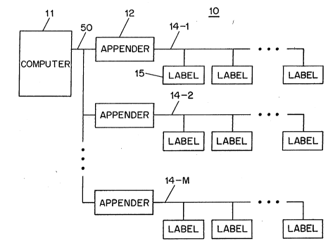
Fig. 1 illustrates an electronic price display
system 10 embodying the principles of the invention. System
10 may be employed in a retail store where goods for sale
are placed on shelves. In Fig. 1, computer 11, which may be
a conventional microcomputer with appropriate bus interface
circuitry, is electrically connected to buses 14
14-2 . . ., and 14-M in a multidrop arrangement, where M is -~;~
an integer whose value is determined by a store planner.
Each of these buses runs along the rail of a store shelf in ~-~
the retail store.
As shown in Fig. 1, a myriad of labels are
electrically connected to the buses. One such label is
label 15 which is electrically connected to bus 14-1 in a
-6-
2 1 ,~
A28919-1586/21879
manner to be described. In this illustrative arrangement,
computer 11 can communicate with the labels through their
respective buses. In addition, a multiplicity of appenders
12 are electrically connected between computer 11 and the
labels. Specifically, one appender 12 is connected to each
bus between computer 11 and the labels of that bus. It
should be pointed out that all of the labels 15 may be
structurally identical to one another, differing only in
their unique bus addresses which are pre-assigned thereto
for identification purposes. Similarly, all of the
appenders 12 may be structurally identical to one another,
differing only in their respective bus addresses. Bus 50
provides a bidirectional communication path between computer
11, also sometimes called a host, and an appender 12.
Illustratively, appender 12 is electrically connected in
such a manner to bus 50. In one embodiment there is an
appender for each four-foot section of shelf rail in the
store. For the purpose of the present discussion, it -`~
suffices to know that the function of an appender in system ~
20 lO is to append its bus address to a message to computer 11 ~ ~-
sent by a label on the same bus as that appender. The
appended bus address enables computer ll to identify which
bus the label that sent the message is on.
Fig. 2 provides the front view of label 15. It
comprises a dual display including display 61a and display
61b which are of a liquid crystal type, light emitting diode
(LED) 6 which is controllable by the label, and push-buttons
5 and 27 whose functions are described hereinbelow. In
addition, case 90 provides mechanical interconnection of the
various parts of label 15.
21~2(~
A28919-1586/21879
Fig. 3 provides the top view of label 15. As
shown in Fig. 3, label 15 has connector 37, whereby the
label can be mechanically snapped onto one of many locations
on the rail (not shown in Fig. 3) to be electrically con-
nected to bus 14-1. On connector 37, springy contacts 31, -
32~and 33 permit reliable electrical connection of label 15
of Figs. 2 and 3 to the bus.
Fig. 4 illustrates a physical disposition of
label 15 and other labels on bus 14-1 on rail 9. Thus, -
label 15 may be used to display the prices of goods close
thereto, which prices are communicated to it from computer
ll (not shown in Fig. 4).
Fig. 5 shows a cross-section of rail 9. Conduc~
tors 41, 42 and 43 run along the length of rail 9 and are
positioned so as to be respectively connected to contacts
31, 32 and 33 of label 15 of Fig. 3.
Fig. 6 shows detailed connections of label 15 to
bus 14-1. Illustratively, bus 14-1 comprises power line 21,
data wire 22 and ground wire 23 which are, respectively,
physically realized as conductors 43, 42 and 41 of rail 9 of ~-~
Fig. 5. Specifically, line 21 transports electrical power ~
from computer 11 (not shown in Fig. 6) to label 15 and other ~ ~'
labels on bus 14-1; wire 22 transports messages between
computer 11 and same; and wire 23 provides a ground or
common line between computer 11 and the same.
Central to label 15 is processor 63 which, in this
illustrative embodiment, comprises microprocessor LC5851N
manufactured by Sanyo Electric Co., Ltd. Processor 63
includes, inter alia: data port 65, read only memory (ROM)
60, random access memory (RAM) 67, and liquid crystal
2~2~
A28919-1586/21879
display (LCD) driver 69. A full description of the
functions and specifications of the microprocessor LC5851N
may be found in a manual No. 3341, which is made available
by Sanyo Electric co., Ltd. Semiconductor Overseas Marketing
Division, and which is hereby incorporated by reference.
~ ROM 60, programmed permanently at the time of
manufacture, contains a monitor program which orchestrates
the basic operation of label 15 to perform different func-
tions required thereof. One of these functions is to com- ;~
municate messages with computer 11 asynchronously through
springy contact 32. To this end, each message communicated
between computer 11 and label 15 is sent to or retrieved
from RAN 67 through the data port 65. The processor 63
properly formats the output messages in a standard serial
protocol and recognizes the input messages in that same
protocol.
EEPROM 70, also connected with processor 63, com-
prises a multiplicity of registers (not shown in Fig. 6). A
particular one of the registers contains the identification
of label 15 which represents its unique address on the bus
in electronic pricing system 10. Other registers include
display registers for storing, for example, price informa-
tion to be displayed by LCD 61a and LCD 61b. EEPROM 70
preferably is a serial-in serial-out shift register memory,
offering the advantage of a small pin count in its connec-
tion with processor 63. The unique identification is
programmed by a several step process -- the address is
accumulated in RAM 67, and then stored in EEPROM 70, in
response to a specific i.nstruction received over the bus.
It is anticipated that for a given label 15, the specific
_g_
2~
A28919-1586/21879
instruction would be given only once, so that the unique
identification remains unchanged during the life of the
label. Alternatively, the unique identification could be
stored in some other form -- jumpers in the printed wiring
board of the label, or masked contents of ROM 60 being two
exàmples.
While EEPROM 70 is shown as a separate piece part
from processor 63, one skilled in the art will appreciate
that one could, without departing from the scope of the
10 invention, employ a processor with a built-in EEPROM ~ -
instead. Other types of memory could be used instead of
those described above. A battery-backed RAM could be used,
for example, to store some or all of what are described
above as stored in EEPROM. The processor's stored program
could be in EEPROM, EPROM, OTPROM, or battery-backed RAM,
for example, rather than the ROM described above.
The messages from computer 11 through data wire 22 -~
to processor 63 may contain display data including informa~
~:,
tion such as the prices of goods, price per unit of goods,
20 etc. Upon receiving such messages in RAM 67, the program -
therein extracts the display data, stores it in EEPROM 70,
and provides it for LCD driver 69 to read. This driver
accordingly provides electrode voltage levels to display the
price and other information on LCD 61a and LCD 61b which are
of conventional design. In this particular illustrative
embodiment, each LCD character on LCD 61a and LCD 61b is
made up of 11 segments which may be individually turned on
or off by LCD driver 69 to realize a display character,
which may be, for example, a numeral or an alphabetical
letter. Each of LCD's 61a and 61b in the present embodiment
--10--
2~2(~
A28919-1586/21879
can display up to 6 characters at a time. In addition, each
LCD has annunciators including, for example, a dot symbol, a
triangle symbol and a square symbol, which may be individ-
ually turned on or off by driver 69 as well.
The display data which determines the on/off
condition of the individual character segments is stored in
display registers of EEPROM 70. As shown in Fig. 7, EEPROM
70 comprises a multiplicity of registers including 4 arrays
of display registers denoted 82a-82h, 83a-83h, 84a-84d and
85a-85d, and two individual display registers denoted 80 and
8~. Other registers within EEPROM 70 are categorically
denoted miscellaneous registers 89. Each display register
of Fig. 7 can buffer up to 6 characters' worth of display
data. In order to provide customers with helpful informa-
tion including, for example, the brand name of a product and
its price, it is oftentimes desired to display a sequence of
more than 6 characters. In this particular embodiment,
there are 4 display sequences which are hereinafter referred
to as display sequences A, B, C and D, and whose data is
20 stored at register arrays 82a-82h, 83a-83h, 84a-84d, and
85a-85d, respectively. This being so, the display sequences
A and B each have a maximum length of 8 registers or 48
characters. The display sequences C and D each have a
maximum length of 4 registers or 24 characters. A particu-
lar display sequence is displayed on LCD 61a or LCD 61b by
having LCD driver 69 read the corresponding register array
in a predetermined order, as will be described.
Referring back to Fig. 6, power line 21 provides
power to label 15 through springy contact 33. The power is
used, for example, to power LED 6 (not shown in Fig. 6)
--11--
2 ~ ~ 2 (~
A28919-1586/21879
supported by conventional LED circuitry 62. Push-button 5
is a conventional switch for allowing a customer to change
the displayed information LCD 61a from, for example, the
price of the goods to their unit price. Push-button 5 when
S pushed creates an electrical signal level to processor 63.
Thè program within ROM 60 polls the button periodically for
detecting any such pressing of the button. Upon detection
of the pressing of button 5, the program retrieves, for
example, alternative price information from EEPROM 70 to be ~ -
displayed by LCD 61a. Similarly, push-button 27, when
pushed, causes LCD 61a to display other information which
includes, for example, maintenance information, supplemen-
tary information for the consumers, etc. Fig. 6 al~o shows -
the connection of ground wire 23 to label 15 through contact
31.
In order for computer 11 to communicate messages
effectively to individual labels for the latter to display
information for the consumers, it is necessary to have an
operative protocol conducive to the effective communica-
20 tions. The format of messages communicated between the ~
labels and computer 11 will now be described. Fig. 8 illus- ;
trates a generalized message. As shown in Fig. 8, the
generalized message is headed by a label address field which
consists of 2 bytes. Specifically, if this message is
transmitted by a label, the label address in that field
indicates which label it is from. Otherwise, if this
message is transmitted by computer 11, the label address
indicates the label for which the message is intended. The ~-
address 0000H (hexadecimal) is reserved for addressing the
labels in system 10 globally.
-12-
2.~ 2~3~
A28919-1586/21879
The label address field is followed by the message
length field which is one byte long. This field indicates
the length of the current message. The knowledge of the
message length is important in that a message is normally -~-
split up and is sent byte by byte. With this knowledge, any
device receiving a message is able to confirm that it has
received a complete message by keeping track of the number ~-
of bytes received.
Following the label address field and the message
length field is the command field which is one byte long.
In messages originating at the computer ll, this field con-
tains a command byte. In messages originating at a label,
the command field contains a status byte indicative of the
status of the label.
The command field is followed by the data field
which is of a variable length. For example, the data field
in a message from computer 11 to a label may contain the
price information.
The last field of the message is the checksum
field which is one byte long. This field, in a conven-
tional manner, enables a message receiver, whether it be
computer 11 or a label, to determine if the message was
received without error.
Of course, the message format depicted by Fig. 8
is for illustrative purposes. Thus, it is appreciated that
a person skilled in the art may devise a different format to
suit a particular application, without deviating from the
invention.
From time to time, computer 11 sends write regis-
ter messages to the labels in system 10 to write new display
-13-
21~2~
A28919-1586/21879
data onto their display registers. A generalized write
register message is shown in Fig. 9. The address field of
this message identifies the label for which it is intended,
and the length byte indicates the length of the message, as
described before. However, in accordance with the inven-
tion, the most significant bit (MSB) of the length byte is
designated as a freeze bit. Each label in system 10 -
includes a freeze flag in EEPROM 70 responsive to the freeze
bit value. A freeze bit of a logic 1 sets the freeze flag ~; -
in the label just identified. With the freeze flag being
set, the label is able to receive multiple related write
register messages, each updating a display register in its
EEPROM, without displaying any of the new information until
the complete set of messages has been received. Thus, the
freeze bit of the length byte is used to indicate whether
additional related messages are to be transmitted to the
label. Specifically, when the freeze flag is set, the label
will be in a freeze mode and driver 69 will stop reading
display data from any display register arrays to prevent an
unintended or meaningless sequence of characters from being
displayed on the label.
During the freeze mode, the label displays on LCD
61a data from register 80 which is used for a temporary
static display register storing price information in this
particular embodiment, and on LCD 61b data from register 81
which is used for a temporary static display register
storing unit price information. This being so, the price
and unit price will always be available to consumers, even
when the freeze bit is on. The label will remain in the
freeze mode until the freeze flag is reset after receiving
-14-
2 ~L ~ 2 ~ ~ h
A28919-1586/21879
particular types of messages issued from computer 11, which
include, for example, read status command messages for
periodically eliciting status information from each label.
When the freeze flag is reset, the label continues with its
updated display sequence.
~ It is noteworthy that, in a situation involving an
update of only one display register, the freeze bit of the
write register message may be a logic zero, without setting
the freeze flag. Accordingly, the display register which is
being updated will have its data changed and used in any on-
going display sequence at the next occurrence of that regis-
ter in that sequence. This advantageously allows a particu-
lar register, such as the one storing a price, to be changed
instantaneously without stopping the display sequence.
Alternatively, the freeze bit may be set if only one display
register is updated if it is desired to temporarily hold the
display in a freeze state.
The write register message is characterized by its
command byte which is in this instance designated llH. As
shown in Fig. 9, the data field of this message contains 10
bytes which include: a display flag nybble (DFN) containing
display flag information to be described (where a nybble
consists of ~ bits), a register identification nybble (RIN)
for identifying the display register for which the new
display data is intended, followed by 9 bytes of display
data representing 6 character words, which are denoted char-
1 through char-6. Each character word is associated with
one of the 6 11-segment characters on an LCD. In accordance
with the invention, each character word consists of a char-
acter flag bit, and 11 data bits representing combinations
-15-
21 ~2~
A28919-1586/21879
of on/off conditions of the corresponding LCD character -
segments to realize different display characters. Specifi-
cally, each of the 11 data bits is associated with a segment -
of the corresponding LCD character. A data bit of a logic 1
5 indicates to LCD driver 69 to turn on or light its associ-
ated segment; otherwise, the segment remains to be turned
off or dark. In this manner, the 11 data bits of a
character word are bit-mapped to the corresponding 11 --~
segments of a LCD character.
The character flag bit of each character word is
used in this particular embodiment to indicate to LCD driver
69 to turn on or off an annunciator (not shown) on an LCD
such as a decimal point, a currency sign, a virgule indica-
tor or a "FOR" sign. Each character flag bit is associated -~
with one such annunciator which is positioned immediately to ;~
the right of the corresponding character. By convention, a ~ ~ -
character flag bit of a logic 1 causes driver 69 to turn the
associated annunciator on and, otherwise, it remains off.
The function of the above-mentioned DFN will now
be described. It is used in this particular embodiment for ~ ~;
promotional or identification purposes to support store
operations. The individual bit patterns of the DFN repre-
sent combinations of ons/offs of the dot symbol, square
symbol and triangle symbol annunciators, and LED 6. The ~ ~
decoding table for the DFN consisting of bit 0 through bit 3 ~ -
is shown in Fig. 10. Any of these bits having a logic 1
will cause driver 69 to turn on the corresponding annun-
ciator, in accordance with the table of Fig. 10. The
remaining checksum byte in Fig. 9 is for error checking
purposes as described before.
,'~
--16--
2 ~h ~
A28919-1586/21879
As mentioned before, each display sequence is
oftentimes longer than 6 characters or one register's worth
of display data. As such, each LCD needs to display a
sequence of characters in parts. Specifically, characters
from a first register in an array corresponding to the
sequence are displayed for a selected period of time,
followed by those from a second register for another
selected period of time, and so on and so forth. Thus, the
individual display periods, which are normally short, are
determined by the dwell time allotted to the registers in
the array. Computer 11 allots such dwell time to each
display register in a label through a write sequence mes-
sage. Fig. 11 shows a generalized write sequence message.
As usual, the first two bytes of this message identify the
label for which the message is intended, followed by a
length byte indicating the length of the message. The MSB
of this length byte is also designated as a freeze bit whose
function is fully described hereinbefore.
The write sequence message is characterized by its
command byte which is designated 12H. Following the command
byte is a sequence control (SEQ CTL) byte identifying which
of the four display sequences A, B, C, and D is being
addressed. In this instance, the display sequence A is
identified by a bit pattern 0001, the sequence B by a bit
pattern 0010, the sequence C by 0011 and the sequence D by
0100. Specifically, the sequence identification is con-
tained in the least significant nybble (LSN) of the SEQ CTL
byte, and the most significant nybble (MSN) thereof is
unused in the present embodiment.
-17-
2 ~
A28919-1586/21879
The SEQ CTL byte is followed by a number of data
bytes. These data bytes identify all or a subset of display
registers in the array corresponding to the identified dis-
play sequence, and the dwell time for each of the registers
just identified. As each data byte is associated with one
of~the display registers constituting the display sequence,
the write sequence message of Fig. 11 having 8 such data
bytes is for the display sequences A and B having a maximum
of sequence length of 8 registers. Of course, the message
is accordingly shorter when a sequence involves fewer than 8
registers. Specifically, the MSN of a data byte contains
identification of a register which, in this instance, ~ -
assumes one Qf the 13 bit patterns OOO1 through 1101, des-
pite the fact that only a subset thereof is used in the
present embodiment. In accordance with another aspect of
the invention, the order of the data bytes in the write
sequence message defines the order of the corresponding
registers to be read by LCD driver 69. The LSN of a data
byte specifies the dwell time for the register identified by
the MSN in the same data byte.
Fig. 12 is a decoding table for the data bytes.
As shown in Fig. 12, each LSN of a data byte is associated
with a different dwell time. The LSN having a bit pattern
1111 indicates to LCD driver 69 to enter a hold state during
which the current display characters will stay on the LCD.
Once in the hold state, LCD driver 69 will not continue to
read the next register in the sequence until either of
buttons 5 and 27 is pressed. The last byte of the write
sequence message of Fig. 11 is the checksum byte whose
function is described hereinbefore.
-18-
2 ~ L 2 ~ ~ ~
A2~919-1586/21879
While the write sequence message defines each dis-
play sequence, a select sequence message from computer 11
selects which ones of the four display sequences A, B, C and
D are to be respectively displayed on LCD 61a and LCD 61b.
Fig. 13 shows a generalized select sequence message. In
this message the command byte, which follows the above-
described address field and length byte, is designated 14H.
Following the command byte are two data bytes. The MSN of
the first date byte identifies a display sequence to be
displayed on LCD 61a, and the LSN identifies a second dis-
play sequence to be displayed on LCD 61b. The MSN of the
second data byte identifies a third sequence to be displayed
on LCD 61a for one sequence when button 5 is pressed, and
the LSN identifies a fourth sequence to be displayed also on
LCD 61a for one sequence when button 27 is pressed. As
before, a bit pattern 0001 identifies the display sequence
A, 0010 the display sequence B, 0011 the display sequence C
and 0100 the display sequence D. The checksum byte of the ~ .
select sequence message is, again, for error checking
purposes as described before.
It is noteworthy that the data bytes of the select
sequence message are stored in EEPROM 70 and are the default
values used in the label on power up to select the sequences
to be displayed on LCD's 61a and 61b in each instance. This
message also clears the freeze flag of a label when set.
The particular selection of the sequences defined -
by the select sequence message may be changed by a modify `-
sequence message issued from computer 11. This message is
generally used to cause a temporary change in the displays -
and particularly used with the global address 0000H to cause
-19- ~ -~
21~,0~
A28919-1586/21879
all labels to simultaneously change to preloaded maintenance
displays in exigent circumstances. As shown in Fig. 14, the
modify sequence message is characterized by its command byte
which is designated 13H. Following the command byte are two
data bytes. The MSN of the first data byte identifies a
display sequence to be temporarily displayed for a predeter-
mined period on LCD 61a, and the LSN identifies a second -~
display sequence to be temporarily displayed on LCD 61b.
Furthermore, the MSN of the second data byte identifies a
third sequence to be temporarily displayed on LCD 61a when
button 5 is pressed, and the LSN identifies a fourth
sequence to be temporarily displayed also on LCD 61a when
button 27 is pressed. The functions of the address field
and the checksum byte of the modify sequence message are ;
described hereinbefore and their description is thus omitted
here. Finally, it should be pointed out that the data bytes
of the modify sequence message, unlike those of the select
sequence message, are stored in RAM 67 and therefore
volatile. ;-~
An example demonstrating the communicative process ;~
whereby computer 11 causes label 15 to display the phrase
"on sale 2¢" on LCD 61a will now be described. In this
example, each of the words "on", "sale", and "2¢" will be
cyclically displayed in a sequential order with a dwell time
of a second. To this end, computer 11 sends to label 15
three individual write register messages, each of whose
formats is identical to that of Fig. 9. Specifically, the
first write register message having a command byte llH
comprises an RIN identifying register 85a, a char-2 having a
bit pattern which will cause LCD 61a to display a character
-20-
2~2~
A28919-1586/21879
"S", a char-3 which will cause the LCD to display a charac-
ter "A", a char-4 which will cause the LCD to display a
character "L", and a char-5 which will cause the LCD to
display a character "E". (The remaining char-1 and char-6
in this instance each assume a bit pattern 000H, thus
ke`eping their corresponding characters turned off.) As
shown in Fig 15, after receiving the write register message,
label 15 stores at register 85a in EEPROM 70 the four bit-
patterns corresponding to the four characters "S", "A", "L"
and "E" constituting the word "SALE". In a similar manner,
the second write register message causes register 85b in the
same array as register 85a to contain bit-patterns corres-
ponding to the word "ON". Finally, the third write register
message from computer 11 comprises an RIN identifying regis-
ter 85d, and a char-4 having a bit pattern such that its
character bit is of logic 1 and the rest of its bit pattern
will cause the LCD to display a numeral "2". In this illus-
trative embodiment, the character bit of a char-4 in a write
register message is associated with the "cent" sign annun-
20 ciator (or ¢). By setting the character bit of the char-4 ;
in the last message to a logic 1, the cent sign annunciator ;~
will be activated on the LCD along with the numeral "2" on ~:
its left.
It should be noted at this point that the words
stored in the register array 85a-85d need not be in the same
order as the words to be displayed. The actual display
order is specified by a write sequence message whose command ~ ~
byte is 12H and whose format is similar to that of Fig. 11.
In this write sequence message from computer ll to label 15, ~;
the least significant nybble of the SEQ CTL byte assumes a
2 ~L ii 2 ~ i-3 ~7~
A28919-1586/21879
bit pattern 0100 indicating that the display sequence D
corresponding to the register array 85a-85d is being speci-
fied. Illustratively, this write sequence message has three
data bytes indicating the order of displays and the dwell
5 times associated therewith. The first data byte has an MSN - -
idèntifying register 85b within the register array 85a-85d,
which indicates that the content of register 85b or the word
"ON" will be displayed first. The LSN of the first data
byte assumes a bit pattern 0001 indicating that the display -~
dwell time of the word "O~" will be a second long, in
accordance with the table of Fig. 12. As a matter of fact,
in this example each LSN of the three data bytes assumes a
bit pattern 0001 because of the equal dwell time of a second
long. Continuing the example, the second and third data
bytes have their MSN's identifying register 85a and register
85d, respectively. This being so, the words "ON SALE 2¢"
will be displayed in that order, as specified by the display
sequence D.
In order to have "ON SALE 2¢" display on LCD 61a
when no button is pressed, computer 11 issues to label 15 a
select sequence message whose command byte is 14H and whose
format is identical to that of Fig. 13. Specifically, the
MSN of the first data byte assumes a bit pattern 0100
indicating that the display sequence D is selected for
display on LCD 61a when neither of buttons 27 and 5 is
pressed. Fig. 16 depicts the time-sequence of displays on
LCD 6la as a result of the communication of the above
messages from computer 11 to label 15.
The foregoing mlerely illustrates the principles of
the invention and those skilled in the art will be able to
-22-
A28919 1586/21879
devise numerous arrangements which, although not explicitly
shown or described herein, embody the principles of the
invention.
For example, label 15 in the above illustrative
embodiment employs a dual display. It may be desirable to
us~e a single display involving LCD 61a only. If such is the
case, the respective data portions in the select sequence
message and the modify sequence message relating to the-~
display on LCD 61b may be ignored.
In addition, the LCD characters on either of LCD's ~ -~
61a and 61b in the illustrative embodiment are made up of -
segments. In the event that the LCD characters are made up
of elements other than segments, such as pixels in an array, -~
the data bits of the character words in the display regis-
ters would be bit-mapped to the individual elements, in
accordance with the invention. -~
Moreover, in the illustrative embodiment register
80 is a freeze display register and is designated to store,
for example, price information for display on LCD 61a during
the freeze mode. However, the designation of such a freeze
display register need not be fixed. In an alternative
embodiment, for example, a data nybble in the select
sequence message of Fig. 13 is used to identify a selected
one of the display registers in EEPROM 70 as the freeze
display register. Illustratively, the LSN of the first data
byte of the select sequence message is used for such
identification purposes. of course, in this alternative
embodiment, the aforementioned function of this LSN to
identify the second display sequence is removed. As a
result; the second display sequence is predeterminedly
-23-
~ ~ 2~13~ ~
A28919-1586/21879
designated to be one of the display sequences A, B, C, and
D. Alternatively, the select sequence message may be
lengthened to include an additional data byte wherein a
nybble thereof is used to identify the second display
sequence, or the freeze display register in the first place.
` Finally, the invention is disclosed herein in a - -
form in which the various functions of system 10 are per-
formed by discrete functional blocks. However, any one or
more these functions could equally well be performed by one
or more appropriately programmed microprocessors, microcoded
integrated circuits, application-specific integrated
circuits, and so on.
-24-