Note: Descriptions are shown in the official language in which they were submitted.
1
File: 44.447
OPTICAL SENSOR CONTROL
Technical Field
This invention relates generally to electronic
optical sensors for monitoring positions of moving
objects, and more particularly, to a method of and
apparatus for controlling the optical sensors to
minimize power consumption.
Background Art
Optical sensors are widely used to determine the
position of moving objects. One example is in an
electricity meter wherein the speed of rotation of an
eddy disk is related to the rate at which electricity
is being consumed. See, for example, U.S. Patent No.
4,827,123 assigned to the assignee of the present
invention.
All optical sensors comprise a light emitter and a
light detector that establish an optical path that
includes a disk or other moving object. The moving
object may either occlude the direct light from emitter
to detector ("opto-interruptor"), or the moving object
may, by virtue of its reflective and non-reflective
areas, modulate the amount of reflected light passing
from emitter to detector (reflective sensor).
Reference is now made to FIG. 1, wherein an
optical sensor 20 comprises a light-emitting diode
(LED) 22 converting an input electrical signal into
light radiation, and a phototransistor 24 which is
sensitive to light radiated by the LED 22. A rotating
2
~~.~,2:~~' 6
meter disk 26 is positioned so as to reflect incident
light radiated by the LED 22 onto the phototransistor
24. The reflecting surface of the disk 26 has
reflective areas 28a which reflect incident light
therefrom, and non-reflective areas 28b which absorb
light rather than reflect it. The conventional
metallic surface of the disk is normally shiny enough
to reflect light without any modification, whereas the
non-reflective areas can be provided through a black
applique applied to the disk. The output of the sensor
is low when the phototransistor 24 is illuminated, and
the output is high when the phototransistor 24 is not
illuminated.
The LED 22 may be always kept on by providing a
' constant current at the input. ' However, the magnitude
of the constant current is limited by the ability of
the LED to operate with continuous excitation.
Alternatively, the LED 22 may be pulsed at
intervals smaller than the expected light-to-dark
period of the rotating disk 26. The intermittent mode
of operation allows the LED to be operated at higher
power to increase peak brightness.
Sensitivity of the optical sensor is defined by a
signal-to-noise ratio R = (S + A)/(N + A), where:
S (signal) is the output phototransistor current
resulting from light reflecting from a reflective area
on the disk,
N (noise) is the output phototransistor current
resulting from light reflecting from a non-reflective
area on the disk, and
A (ambient) is the output phototransistor current
resulting from background light.
In order to maximize R, the peak brightness should
be as high as possible. Thus, the intermittent mode of
CA 02112166 2004-02-20
operation allows a signal-to-noise ratio to be increased to improve
sensitivity of optical
sensors.
However, this mode of operation requires significant amount of power to be
applied to the sensor in order to provide permanent LED pulsing with high peak
brightness. Furthermore, permanent LED pulsing with high peak brightness
results in
reducing the mean time to failure (MTTF) of the LED, which is the average time
before
first failure of the LED. The MTTF is a measure of the reliability of the LED
and the
entire optical sensor.
In view of the above, it would be desirable to provide a method of and
apparatus
for controlling optical sensors to reduce power consumption without decreasing
sensitivity. It would also be desirable to increase reliability of the optical
sensor by
increasing the mean time to failure of the LED.
Disclosure of the Invention
Accordingly, one advantage of the invention is in reducing the power
consumption of an optical sensor without decreasing sensitivity.
Another advantage of the invention is in improving the reliability of an
optical
sensor by increasing the mean time to failure of the LED.
The above and other advantages of the invention can be achieved, at least in
part, by providing an optical sensor with a control circuit which is
responsive to an
output signal generated by a light detector for causing a light emitter to
suspend
radiation of light. In accordance with one aspect of the invention, there is
provided an
optical sensor for monitoring position of the movable means comprising:
light-emitting means for radiating light,
light-receiving means for sensing the light radiated by said light-emitting
means
and providing an output signal corresponding to received light, and
control means responsive to the output signal for causing said light-emitting
means to suspend radiation of the light,
said movable means being positioned so as to provide incidence of the light
radiated by said light-emitting means on said light-receiving means in at
least one first
CA 02112166 2004-02-20
4
time interval and to prevent, at least in part, the light radiated by said
light-emitting
means from falling on said light receiving means in at least one second time
interval.
A control circuit may comprise a threshold circuit which causes the light
emitter
to suspend radiation of the light in response to a predetermined level of the
output
signal under reflective conditions (i.e. when the incident light is reflected
from a
reflective area of a meter disk). During the reflective period, the threshold
circuit turns
off the LED as soon as the output of the phototransistor goes below a
threshold level
signifying that the light detector has been turned on. Therefore, no more
power is used
in the LED than is necessary to transmit the light signal to the
phototransistor. The
invention accordingly can enable power consumption under the reflective
conditions to
be minimized.
The control circuit may comprise a timer circuit, which under non-reflective
conditions (i.e. when the incident light is absorbed by a non-reflective area
of a disk),
turns off the LED after expiration of a predetermined time interval. During
the non-
reflective period the output signal of the phototransistor remains high. The
predetermined time interval can be chosen to be slightly longer than the
response time
of the phototransistor, which is known and independent of temperature for a
given type
of phototransistors. Thus, during the non-reflective period the timer circuit
leaves the
LED on only for a short time interval required to make sure that the
phototransistor is
off. Accordingly, it is possible to minimize power consumption under non-
reflective
conditions.
As the LED is on only for small portions of reflective and non-reflective
periods, the mean time to failure (MTTF) of the LED is increased. As a result,
the
reliability of the optical sensor can be significantly improved.
In accordance with a preferred embodiment of the invention the LED is
supplied with intermittently interrupted electric energy produced by a driving
oscillator.
The pulse-repetition period of the driving oscillator is less than intervals
when the LED
is turned off by the control circuit. The driving oscillator is responsive to
a
predetermined level of the output signal of the phototransistor for turning
off the LED
during the reflective period. Furthermore, the driving oscillator turns off
the LED after
a predetermined time interval during the non-reflective period.
CA 02112166 2004-02-20
The control circuit may also include a holding circuit which maintains a
steady
level of an output signal of the sensor for a preset time period. The holding
circuit
prevents the output signal from multiple transitions during a short time
interval. The
preset time period may be chosen so as to allow the next change in output
state to occur
only after three consecutive reflective or non-reflective periods.
In accordance with another aspect of the invention there is provided an
optical
sensor for monitoring position of a movable member comprising:
a light-emitting device for converting supplied electric energy into light,
a photocell actuated by the light radiated by the light-emitting device for
producing an output electric signal corresponding to received light,
a driving circuit coupled to said light emitting device for supplying said
light-
emitting device with intermittently interrupted electric energy,
a control circuit coupled between said photocell and said light-emitting
device
for causing said light-emitting device to suspend radiation of the light in
response to
said output signal,
said movable member being positioned so as to provide incidence of the light
radiated by said light-emitting device on said photocell in at least one first
time interval
and to prevent, at least in part, the light radiated by said light-emitting
device from
falling on said photocell in at least one second time interval.
In accordance with the method of the invention, the following steps are
carried
out. The method of monitoring moving objects using a light emitter and a light
detector
provides:
radiating light from the light emitter,
sensing the radiated light by a light detector for producing an output signal,
positioning the movable object so as to provide incidence of the light
radiated
by the light emitter on the detector in at least one first time interval and
to prevent, at
least in part, the light radiated by the light emitter from falling on the
detector in at least
one second time interval,
suspending the radiating in response to a predetermined level of the output
signal during the first time interval, and
CA 02112166 2004-02-20
6
suspending the radiating after expiration of a predetermined time period
during
the second time interval.
The invention may be practiced with the movable object that rotates so as to
reflect the radiated light during the first time interval and to absorb the
radiated light
during the second time interval. For example, a disk having a reflective
surface with
reflective and non-reflective areas may be used as such a movable object.
Also, the invention may be practiced with the movable object that rotates so
as
to pass the radiated light during the first time interval and to interrupt the
radiated light
during the second time interval. For example, a toothed wheel having a
plurality of
teeth for interrupting the radiated light may be used as such a movable
object.
Still other advantages of the present invention will become readily apparent
to
those skilled in this art from the following detailed description, wherein
only the
preferred embodiment of the invention is shown and described, simply by way of
illustration of the best mode contemplated of carrying out the invention. As
will be
realized, the invention is capable of other and different embodiments, and its
several
details are capable of modifications in various obvious respects, all without
departing
from the invention. Accordingly, the drawing and description are to be
regarded as
illustrative in nature, and not as restrictive.
Brief Description of the Drawinas
FIG. 1 is a schematic diagram of a prior art
optical sensor.
FIG. 2a is a diagram illustrating sensor mounting.
FIG. 2b is a diagram illustrating use of a collar
to prevent reflected sunlight saturation.
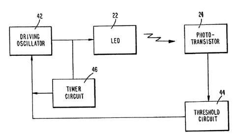
FIG. 3a is a block-diagram showing a feedback
control strategy according to the preferred embodiment
of the present invention.
FIG. 3b is an electrical diagram of an optical
sensor with control circuitry according to the
preferred embodiment of the present invention.
FIG. 4 is a diagram showing waveforms illustrating
operation of the control circuitry shown in FIG. 3b.
Best Mode For Practicing the Invention
Reference is again made to FIG. 1 of the drawings
showing a typical optical sensor 20 of a type that may
be incorporated in an electricity meter. In accordance
with the preferred embodiment of the invention, the
optical sensor 20 may be a Siemens SFH900 miniature
light reflection emitter/sensor which consists of a
single infrared light-emitting diode (LED) 22 and an
NPN phototransistor 24 mounted in a single plastic
package. The SFH900 is a three terminal device having
an LED anode, phototransistor collector and common
ground terminal. The rotating disk 26 is positioned so
as to reflect incident light radiated by the LED onto
the phototransistor. In an electricity meter, the
separation distance between the reflective surface of
the meter disk and the,sensor is ideally 1 mm (.040"),
however sensitivity is approximately 20% of optimum
over the range of .5 mm to 4 mm (.020" to .15"). The
non-reflective areas 28b are represented by black bars,
8
whose width should be at least 10 mm (.4") to
accommodate the maximum sensor distance of .1".
Due to the reflection of sunlight off the meter
disk, shown in FIG. 2a, performance of the sensor may
be ensured in full sunlight, in accordance with one
aspect of the invention, by providing it with an
absorptive collar 32, as shown in FIG. 2b. This collar
32 is a thin flat piece of black material, which
prevents reflected sunlight from falling on the sensor
and saturating the phototransistor as tends to occur in
the prior art arrangement of FIG. 2a. The collar may
be, for example, about 1" in diameter to ensure that no
multiple reflections of incident sunlight can fall on
the phototransistor.
Reference is now made to FIG. 3a illustrating a
feedback control strategy according to the preferred
embodiment of the present invention. A LED 22 is
supplied with intermittently interrupted electric
energy produced by a driving oscillator 42. When the
light reflected from a reflective area 28a on the disk
26 falls on a phototransistor 24, the output of the
phototransistor goes low. When the output of the
phototransistor goes below a threshold level signifying
that the LED has been turned on, a threshold circuit 44
~ coupled to the output of the phototransistor interrupts
the driving oscillator 42 to turn off the LED 22.
Therefore, no more power is used in the LED than is
necessary to transmit the light signal to the
phototransistor.
Under non-reflective conditions when the light is
absorbed by a non-reflective area 28b of the disk 26,
the output of the phototransistor 24 remains high. A
timer circuit 46 connected to the output of the driving
oscillator 42 interrupts the driving oscillator 42 to
9
turn off the LED 22 after expiration of a preset time
period after the previous interruption of the driving
oscillator. The preset time period is made slightly
longer than the response time of the phototransistor.
Accordingly, during the non-reflective period the timer
circuit 46 leaves the LED 22 on only for a short time
interval required to make sure that the phototransistor
is off.
Reference is now made to FIG. 3b showing a
schematic diagram of the optical sensor provided with
control circuitry according to the preferred embodiment
of the present invention. As the SFH900 optical sensor
uses CMOS logic levels, any output voltage of the
sensor above 3.5 volts is represented by a logic 1, any
output voltage below 1.5 volts'is represented by a
logic 0. Supply voltage for CMOS circuitry is equal to
5 volts.
During non-reflective periods when the light
radiated by the LED 22 is absorbed by a non-reflective
20. area 28b of the disk, the phototransistor 24 is off.
Its collector voltage remains high. Therefore, under
non-reflective conditions the output voltage of the
sensor is represented by a logic 1. Under the worst
case conditions the output voltage should not fall
below 3.5 volts if the reflective surface is black.
Since the supply voltage is +5 volts, the voltage drop
across current sensing resistor R1 must be less than
1.5 volts.
During reflective periods when the light reflected
from a reflective area 28a on the disk falls on the
phototransistor 24, this light causes a photocurrent
equal to about 2 mA to flow in the phototransistor. As
a result, its collector voltage drops to about 1 volt.
Therefore, under reflective conditions the output
to
' 2~.~.~:~~96
voltage of the sensor is represented by a logic 0.
According to the preferred embodiment of the
invention, the control circuitry of the optical sensor
is designed around a 4093 Quad 2-input NAND gate with
Schmitt trigger. The 4093 circuit comprises four 2-
input NAND gates 1-4. The control circuitry comprises
a 120 Hz resistance-capacitance (R-C) oscillator formed
by the HAND gate 1 in conjunction with resistor R6 and
capacitor C1. The R-C oscillator is used for pulsing
the LED 22 in order to provide intermittent light with
increased peak brightness.
The rate at which the LED must be pulsed depends
on the rate, at which the disk rotates, and on the
number of the non-reflective areas on the disk. The
rotation rate of a J-5 meter disk used in the preferred
embodiment of the invention is 111.111 RPM or 1.85185
Hz. To determine the LED pulse rate, the width of the
non-reflective areas on the disk must be considered.
As indicated above, the width of a black bar
representing a reflective areas should be lOmm (.4")
minimum to allow for the maximum distance between
sensor and disk, which is 4mm (.15"). The pattern of
bars is assumed to be 6 equal width bars around the
disk separated by a distance equal to their width.
Each bar will subtend a 30° angle (~r/6 radians). The
disk diameter is 3.75". Assuming that the sensor is
located..625" from the outer edge of the disk, at a
1.25" radius, the width of a bar (or space) at that
,point is .66". Since .4" minimum width is needed, a
pulse must occur before the bar moves .26" (_ .66"-
.4"). Therefore, there must be at least 31 pulses of
the LED for every disk revolution. With a disk angular
rate of 1.85 Hz, the minimum required LED pulsing rate
is then 31x1.85 = 57.3 Hz. To provide some margin, a
11
' ~~~.~~,~~
120 Hz pulsing rate is selected.
The R-C oscillator pulses the LED through a
Darlington circuit T1, which supplies the LED with
driving current. In accordance with the preferred
embodiment of the invention, MPSA-13 circuit
manufactured by Motorola or General Electric may be
used as the Darlington circuit T1. Resistor R2 limits
the LED driving current.
When the light reflected from a reflective area on
the disk falls on the phototransistor, the collector of
the phototransistor is pulled low. A threshold control
circuit-formed by the NAND gate 2 detects this
transition in order to turn off the LED. The collector
of the phototransistor is connected to input 5 of the
NAND gate 2. As shown in FIG.~4, when the collector
drops to a predetermined threshold level Uth at time
tl, the low level of the input 5 equal to the level Uth
causes output 4 of the HAND gate 2 to go high. The
output 4 of the NAND gate 2 is connected through diode
D1 to one of the inputs of the NAND gate 1, which forms
the LED pulsing R-C oscillator. As a result, the high
level at the output 4 of the NAND gate 2 cuts off the
positive half-cycle of the oscillator, and the LED
suspends the radiation of the light.
Thus, during a reflective period the LED is turned
off immediately when the phototransistor signals that
sufficient light has been reflected to exceed the logic
threshold. Therefore, the LED is on for the minimum
time possible. No more power is used in the LED than
is necessary to transmit the light signal to the
phototransistor. The invention accordingly enables
power consumption under the reflective conditions to be
minimized.
If a non-reflective area of the disk is in the
12
~~~.2:~G~~
phototransistor's field of view, the collector of
phototransistor remains high. However, a timer circuit
formed by the NAND gate 3, resistor R5 and capacitor C2
turns off the LED 22 after expiration of a
predetermined time period r, which is equal to the time
constant R x C, where R is the resistance of the
resistor R5, and C is the capacitance of the capacitor
C2. The time constant is made slightly longer than the
response time of the phototransistor, which is known
and independent of temperature for a given type of
phototransistorc. The HAND gate 3 is connected to
input 6 of the NAND gate 2. The resistor R5 and the
capacitor C2 are coupled through diode D3.
As shown in FIG. 4, at time t2 after the
predetermined time period r after the time tl, the
input 6 of the NAND gate 2 goes low, driving high the
output 4 of the NAND gate 2. As indicated above, the
high level at the output 4 of the NAND gate 2 cuts off
the positive half-cycle of the oscillator. As a
result, the LED suspends the radiation of the light.
In accordance with the preferred embodiment of the
invention the predetermined time period is equal to 500
microseconds.
Thus, during a non-reflective period the timer
circuit leaves the LED on only for a short fixed time
period, which is chosen so as to make sure that the
phototransistor is off. The invention accordingly
makes it possible to minimize power consumption under
the non-reflective conditions.
The threshold and timer circuits provides
reduction to one-twentieth of the LED's original duty
cycle. That is, the LED is on only 5% of the total
time. Accordingly, the mean time to failure (MTTF) of
the LED is significantly increased.
13
In accordance with the preferred embodiment of the
invention, to prevent the output of the sensor from
multiple transitions, the control circuitry comprises a
holding circuit formed by the NAND gate 4, resistors
R4, R7, R8 and capacitor C3.
The NAND gate 4 forms the sensor output signal at
its output. The capacitor C3 is coupled to one of the
inputs of the NAND gate 4 to limit the rate at which
the voltage on this input can change. For a low-to-.
high transition of the NAND gate 4, the capacitor C3 is
discharged through resistor R8, coupled to the output
of the NAND gate 3. The capacitor C3 is connected to
the resistor R8 through diode D2. The capacitor C3 can
be discharged when the output of the NAND gate 3 is
low. The fraction of time when~the output of the NAND
gate 3 is low is set by the discharge time constant of
the capacitor C2, which is discharged through the
resistor R7. For a high-to-low output transition of
the NAND gate 4, the capacitor C3 is charged through
the resistor R4 coupled to the second input of the HAND
gate 4. The time constants of the capacitor C3
charging and discharging are chosen to prevent the NAND
gate 4 output state changes at intervals of less than
.025 sec. This .025 sec. interval is equal to three
pulse periods of the LED pulsing oscillator.
Therefore, three consecutive reflections (or non-
reflections) are necessary before the sensor output
state can change.
Thus, the output signal of the sensor indicates
whether a reflective or non-reflective area of the disk
is in the sensor's field of view. As discussed above,
a reflective area is represented by a logic 0, and a
non-reflective area is represented by a logic 1. A
transition of the output from 1 to 0 or from 0 to 1 is
14
~~~.~:~.u~
registered by a processor (not shown) for determining
the disk angular position and/or rotation direction.
Although the preferred embodiment of the invention
is disclosed in connection with a movable object that
rotates so as to reflect or absorb incident light, the
invention may be practiced with the movable object that
rotates so as to pass the radiated light during a first
time interval and to interrupt the radiated light
during a second time interval. For example, a toothed
wheel having a plurality of teeth for interrupting the
radiated light may be used as such a movable object.
There accordingly has been described an optical
sensor for monitoring position of a disk having
reflective and non-reflective areas. The sensor
comprises a LED, a phototransistor and control
circuitry, which is responsive to an output signal
generated by the phototransistor for causing the LED to
suspend radiation of light. When the light reflected
from a reflective area falls on a phototransistor, the
control circuitry turns off the LED as soon as the
output of the phototransistor goes below a threshold
level signifying that the phototransistor has been
turned on. When the light is absorbed by a non-
reflective area and the phototransistor is not turned
on, the control circuitry turns off the LED after a
predetermined time period, which is chosen to be
slightly larger than the response time of the
phototransistor.
The invention accordingly makes it possible to
minimize power consumption of the sensor under the
reflective and non-reflective conditions and to improve
the reliability of the sensor due to increasing mean
time to failure of the LED.
In this disclosure, there is shown and described
15
only the preferred embodiment of the invention, but it
is to be understood that the invention is capable of
changes and modifications within the scope of the
inventive concept as expressed herein.