Note: Descriptions are shown in the official language in which they were submitted.
,2~2316
FIELD OF THE INVENTION:
This invention relates to microprocessors,
micro computers, micro controllers and other free
running clock driver state control logic hereafter
called a control, and in particular to a reset circuit
therefor.
BACKGROUND TO THE INVENTION:
Upon being powered up, both D.C. power and a
clock signal from a clock source are applied to a
control. The control is required to be reset once the
power and the clock signal have become stabilized.
Usually the reset signal (the release of an inhibit ---
logic level) is required to be present for a longer
period of time than it takes for the control's clock
source to become stable, in order to ensure that reset
of the control does not occur until the clock source has
stabilized. Typically a resistor/capacitor timing
circuit is used, the voltage of which operates a Schmitt
trigger. The output of the Schmitt trigger provides the
reset signal.
With a simple timed reset source as described
above, there is no physical guarantee that the clock is
fully operational before the reset is provided. This
can have serious consequences in many cases, where the
control is used to operate a public utility e g. a
telephone switching system.
By the term applying a reset signal to a
control or other device, it is meant that the proper
polarity of a reset DC level or pulse is applied which
will remove an inhibit logic level from a reset or `
inhibit terminal of the control. Therefore it should be
understood that the application of a reset signal could
be construed equally effectively as meaning the removal
of a reset signal or the provision of a reset signal, in
order to allow the processor to operate.
-2- 211~316
SUMMARY OF THE INVENTION:
In accordance with the present invention, the
clock signal is itself used as a source of energy for a
reset timer, rather than the power supply. The clock
signal is DC restored, rectified and then charges a
resistor-capacitor timer which preferably has a bleed
off resistor or other current leakage path which removes
the charge from the capacitor in the timer at a slightly
slower rate than that at which the timer is charged. A
diode clamp is preferably used to discharge the
capacitor if power drops, as in a normal reset circuit.
In accordance with an embodiment of the
invention, a reset circuit is comprised of a DC power
sQurce, a clock signal source, apparatus for applying ~ ~`
power from the power source to the clock source, a timer
apparatus, apparatus for initiating timing by the timer
apparatus from clock signals from the clock signal ~-~
source, and apparatus for generating a reset signal
following a predetermined interval timed by the timer
apparatus.
In accordance with another embodiment of the
invention, a reset circuit is comprised of apparatus for
receiving an oscillatory or clock signal and apparatus
for generating a reset signal therefrom.
BRIEF DESCRIPTION OF THE DRAWINGS:
A better understanding of the invention will
be obtained by reference to the detailed description
below, in conjunction with the following drawings, in
which:
Figure 1 is a schematic diagram of a prior art
reset circuit,
Figure 2 is a schematic diagram of an
embodiment of the present invention,
` 211'~316
-3-
Figure 3 is a graph illustrating wave forms
found in various portions of the circuit of the
invention, and
Figures 4, 5 and 6 are block diagrams
illustrating additional embodiments of the invention.
DETAILED DESCRIPTION OF THE INVENTION:
Figure 1 illustrates a prior art reset circuit
used for a control. A DC power supply source +, which
powers clock 9 and a control (not shown) to be reset,
passes current through resistor 1 to charge capacitor 3.
As capacitor 3 charges, at a particular voltage a
Schmitt trigger, which is connected to the junction of
the resistor and capacitor, operates. Its output signal
is inverted in inverter 7, and the output of inverter 7
is a /RESET signal for the control. This resets the
control, which operates in a well known manner to
operate an initialization program.
While the DC power supply may or may not be
stable, the charging of the capacitor proceeds in any
event, and at a particular time the reset signal
releases the control. However the clock signal source,
which also operated from the power supply, may or may
not be operating, or may or may not be stable by the
time the /RESET is present. Thus the control is reset
under uncertain conditions.
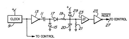
Figure 2 illustrates a schematic diagram of
the present invention. The power source + which powers
the control is applied to clock source 9. The clock
signal line is AC coupled by means of capacitor 11 and
buffer 13 (which could be inverting or non-inverting) to
a DC restorer and rectifier comprised of diode 15 and
diode 17 which are serially connected and similarly
poled. Diode 15 has its anode connected to ground, and
capacitor 11 is connected to the junction of the two
diodes.
~4- 211~31~
The cathode o~ diode 17 is connected to a
resistor-capacitor timing circuit with the cathode of
diode 17 being connected from one end of resistor 19 and
capacitor 20 connected to the other end of resistor 19
to ground. A high-value bleed off resistor 21 is
connected in parallel with capacitor 20.
The junction of resistor 19 and capacitor 20
is connected to the input of Schmitt trigger 23, the
output of which is connected through inverter 25 to a
lo reset line 27.
Another diode 29, having its anode connected
to the junction of resistor 19 and capacitor 21 has its
cathode connected to the power supply terminal +.
In operation, when the system is turned on,
the power supply voltage level increases. The clock
source 9 begins operation. The clock signal is AC
coupled to the DC restorer and rectifier comprised of
diodes 15 and 17 where it is converted to D.C.. The
resulting DC signal is applied to the resistor-capacitor
timer which operates in a manner similar to that of the
prior art, charging capacitor 20. Once charged to a
predetermined level, the Schmitt trigger 23 operates,
the signal, or an inverted version thereof provided by
the operation of the inverter 25, being presented on
reset line 27, which is applied to the processor.
It may be seen that the capacitor 20 only
begins charging once clock pulses are being generated.
Therefore not only will capacitor 20 not charge if the
clock does not operate, contrary to the prior art
circuit described above, but since it is the clock
pulses themselves which cause capacitor 20 to charge,
the delay in the voltage across the capacitor 20 rising
to the threshold voltage for the Schmitt trigger to
operate provides ample time for the clock signal to
become stabilized.
- 2112316
In the prior art, the reset signal, being
enabled due to the presence of the power supply voltage,
could be present either before the clock source has
begun to be operational, or during the first cycle or
few cycles of the clock source when it may be unstable.
This cannot happen in the present invention, since it is
the existence of the clock signal itself for a period of
time which causes the reset signal to be generated.
As a safety factor, diode clamp 29 will be
lo forward biased if the main power supply drops,
discharging capacitor 21 and causing the /RESET signal
to be logically removed.
Resistor 21, in bleeding off charge from
capacitor 20, ensures that if the clock 9 stops, the
voltage across capacitor 20 will drop, causing the
Schmitt trigger to logically remove the /RESET signal
from line 27, stopping the control.
In a successful embodiment, resistor 19 was
lOOK ohms, capacitor 20 was .l~F, capacitor 11 was .l~f
and diodes 15 and 17 were type lN4148. Resistor 21 was
1 megohm.
It will be recognized that the circuit will
operate without resistor 21 or diode 29 being present.
The circuit will also operate with another resistor in
series with diode 15, and of course for a particular
application, different component values may be chosen.
Those skilled in the art will readily
recognize that resistor 19 and capacitor 21 along with
their optionally associated components, comprise a timer
apparatus. In an alternate embodiment of the invention,
the timer apparatus could be comprised of a capacitive
charge storage element charged and discharged by current
sources and current sinks. In another alternate
embodiment of the invention as shown in Figure 4, the
timer apparatus could be comprised of a digital counter
-6- 2112316
39 which might be incremented by pulses from the clock
source 9, and could optionally be decremented by pulses
from a second clock source 41 at some frequency
substantially lower than the frequency of the first -
clock source.
It is also possible to replace the timing
function of resistor 19, capacitor 21 with a counting
chain directly operating from the buffer 13.
It may be further recognized that capacitor
11, diode 15, and diode 17 comprise an apparatus for
initiating timing by the timer apparatus from clock
signals from the clock signal source. In an alternate
embodiment of the invention, as shown in Figure 5, the
apparatus for initiating timing by the timer apparatus
from clock signals from the clock signal source could be
comprised of current source 43 gated by a monostable
multivibrator 45 triggered by pulses from said clock
signal source, as shown.
The entire time delay circuit could
alternatively be replaced with a counting chain 47,
while diode 27 and resistor 21 could be replaced by a
diode 49 reset to the chain, and a missing pulse
detector 51 respectively, as shown in Figure 6.
Figure 3 illustrates signals at various places
of the circuit of Figure 2. Curve A illustrates a curve
which represents the output voltage of clock source 9.
In curve A, prior to operation of the clock, no clock -~
pulses appear as shown at 31. Once the clock source
begins operation, the extremes of the clock signal
pulses as shown at 33 are evident.
The voltage across capacitor 21 is illustrated
as curve B, which begins to rise as shown at 35 once ;
clock signals have been generated by clock source 9.
Curve C illustrates the RESET signal at the output of
Schmitt trigger 23. The stepped voltage 37 occurs at a
: ~ : . .
" . , ,
~7~ 2112316
time following the beginning of the operation of the
clock, and is determined by the threshold of operation
of the Schmitt trigger and the rate of increase of
voltage across capacitor 21.
s While this circuit has been described as
providing a reset circuit for a control, it could
alternatively be used to monitor the loss of any
continuous or almost continuous clock or changing data
stream. The timing apparatus and the apparatus for
lo initiating timing by the timer means from the clock
signal source, might, of course, comprise any
appropriate combination of analog or digital circuit
elements. The resistors can be solid state channels or
o~ther current limiting sources, and the capacitors could
be any circuit or element which exhibits capacitance.
A person understanding this invention may now
conceive of alternative structures and embodiments or
variations of the above. All of those which fall within
the scope of the claims appended hereto are considered
to be part of the present invention.