Note: Descriptions are shown in the official language in which they were submitted.
LASER DIODE ELEMENT WITH EXCELLENT
INTERMODULATION DISTORTION CHARACTERISTIC
Backg~ound~of the Invention:
This invention relates to a laser diode element
and, particularly, to a Distributed Feed Back (DFB) laser
diode element.
A conventional laser diode element of the type
described generally comprises a semiconductor block which
has a front facet, a rear facet opposite to the front
facet, a laser cavity formed between the front and the
rear fac.ets and having a predetermined length L, a
plurality of coating layers coated on the front and the
rear facets to provide a predetermined reflectivity,
respectively, an active layer and a grating formed in the
direction of the laser cavity and coupled to each other
at a predetermined coupling constant ~.
Many types of the DFB laser diode elements have
been developed to have good single longitudinal mode
characteristics.
For example, some DFB laser diode elements have
been proposed in Japanese patent application laid-open
No. Hl-155677, H2-90688, and H2-20087. In these
examples, the predetermined reflectivity as well as a
product of the predetermined coupling constant ~ and the
- 2 ~
predetermined length L in each DFB laser diode element
are optimized from each point of view.
On the other hand, an another DFB laser diode
element has been proposed in Japanese patent application
5 laid-open No. Sho 62-219684. As illustrated in the
drawing of the laid-open paper, the DFB laser diode
element includes a partial grating having a regular
corrugation kept in contact with the front facet.
In the interim, a DFB laser diode element has
10 recently been used as a light source for an analog
modulation in a subcarrier multiplexing optical
transmission method, or the like.
When used as such a light source for the analog
modulation, the DFB laser diode element is required to
15 have a better intermodulation distortion characteristic.
For example, in the field of a mobile communication
system, the DFB laser diode element is desired to have a
characteristic in which 3rd intermodulation distortion
(IMD3) is sufficiently small.
However, any of the conventional laser diode
elements mentioned above have never been fabricated on
the purpose of the analog modulation. Accordingly, no
consideration has been made about intermodulation
distortion characteristics in the conventional laser
25 diode elements. As a result, even when the conventional
laser diode elements are used as light sources for the
analog modulations, a yield in getting laser diode
elements with sufficient intermodulation distortion
characteristics is inevitably not so good.
Summary of the Invention:
It is therefore an object of this invention to
provide a laser diode element which has an excellent
5 intermodulation distortion characteristic and a method of
manufacturing the same.
It is another object of this invention to provide
a laser diode element of the type described which can be
manufactured in a good yield and a method of
10 manufacturing such a laser diode element.
According to an aspect of this invention, there
is provided a laser diode element comprising: a
semiconductor block having: a first end surface; a second
end surface opposite to the first end surface; a laser
15 cavity which is formed between the first and the second
end surfaces and which has a predetermined length L; a
plurality of coating layers which are coated on the first
end surface to provide a reflectivity smaller than 5 %;
and an active layer and a uniform grating which are
20 formed in the direction of the laser cavity and which are
coupled to each other at a predetermined coupling
constant K; the laser diode element being specified by a
product of the predetermined coupling constant ~ and the
predetermined length L and falling within a range between
25 0.4 and 1.0, both inclusive.
The product of the predetermined coupling
constant ~ and the predetermined length L may preferably
fall within a range between 0.5 and 0.7, both inclusive.
The reflectivity may be not greater than 1 %.
The laser diode element may further comprise a
plurality of additional coating layers which are coated
on the second end surface to provide a reflectivity not
5 smaller than 50 %.
The reflectivity provided by the additional
coating layers may be preferably not smaller than 90 %.
According to another aspect of this invention,
there is provided a laser diode element comprising: a
10 semiconductor block having: a first end surface; a second
end surface opposite to the first end surface; a laser
cavity which is formed between the first and the second
end surfaces and which has a predetermined length L; an
active layer and a partial grating which are formed in
lS the direction of the laser cavity and which are coupled
to each other at a predetermined coupling constant ~; the
partial grating being nearer to one of the first and the
second end surfaces than to the other of the first and
the second end surfaces and being remote from the one of
20 the first and the second end surfaces to divide the
direction of the laser cavity into a short length side
and a long length side with the partial grating
interposed therebetween.
According to still another aspect of this
25 invention, there is provided a method of manufacturing a
laser diode element comprising the steps of: uniformly
coating a photoresist layer onto a semiconductor
substrate; partially forming a grating pattern on the
photoresist layer by holographic lithography method;
selectively emitting light onto an area in which a
grating is not formed to make the area exposed; etching
the semiconductor substrate with the grating pattern
5 operable as an etching mask to form the grating; forming
a guiding layer to make the grating buried therein;
growing an active layer on the guiding layer; and forming
a clad layer on the active layer.
Brief Description of the Drawing:
Fig. 1 shows a graphical representation for use
in describing a relationship between yield and ~L in
several examples according to the present invention;
Fig. 2(a) shows a graphical representation for
use in describing a relationship between yield and
15 reflectivity on a front surface in several examples
according to the present invention;
Fig. 2(b) shows a graphical representation for
use in describing a relationship between yield and
reflectivity on a rear surface in several examples
20 according to the present invention;
Fig. 3(a) shows a graphical representation for
use in describing a relationship between normalized
efficiency and reflectivity on a front surface in several
examples according to the present invention;
Fig. 3(b) shows a graphical representation for
use in describing a relationship between normalized
efficiency and reflectivity on a rear surface in several
examples according to the present invention;
Figs. 4(a) through (d) show in schematic vertical
sections a laser diode element during progress of a
method of manufacturing the laser diode element according
to the first embodiment of the present invention;
Fig. 5 shows a band diagram of active layers of
the laser diode element according to the first embodiment
of the present invention;
Fig. 6 schematically shows in vertical section a
side view of a laser diode element according to the
10 second embodiment of the present invention;
Fig. 7 schematically shows in vertical section a
side view of a laser diode element according to the third
embodiment of the present invention;
Fig. 8 shows an electrical field distribution in
15 the direction of a laser cavity in the laser diode
element illustrated in Fig. 7 in comparison with the
conventional one;
Fig. 9 schematically shows in vertical section a
side view of a laser diode element according to the
20 fourth embodiment of the present invention;
Fig. 10 shows an electrical field distribution in
the direction of a laser cavity in the laser diode
element illustrated in Fig. 9 in comparison with the
conventional one;
Fig. 11 schematically shows in vertical section a
side view of a laser diode element according to the fifth
embodiment of the present invention;
7 ~4~
Fig. 12 shows a graphical representation for use
in describing a relationship between yield and coupling
constant ~ in the laser diode element illustrated in Fig.
11 in comparison with the conventional one;
Figs. 13(a) through (e) show in schematic
vertical sections a laser diode element during progress
of a method of manufacturing the laser diode element
according to the second embodiment of the present
invention;
Fig. 14 shows a band diagram of active layers of
a laser diode element according to the second embodiment
of the present invention;
Fig. 15 schematically shows in vertical section a
side view of a laser diode element according to the
15 second embodiment of the present invention;
Figs. 16(a) through (d) show in schematic
vertical sections a laser diode element during progress
of a method of manufacturing the laser diode element
according to the third embodiment of the present
20 invention;
Fig. 17 schematically shows in vertical section a
side view of a laser diode element according to the third
embodiment of the present invention;
Fig. 18 schematically shows in vertical section a
25 side view of a laser diode element according to the third
embodiment of the present invention;
Figs. l9(a) through (d) show in schematic
vertical sections a laser diode element during progress
of a method of manufacturing the laser diode element
according to the fourth embodiment of the present
invention;
Fig. 20 schematically shows in vertical section a
5 side view of a laser diode element according to the
fourth embodiment of the present invention;
Fig. 21 schematically shows in vertical section a
side view of a laser diode element according to the fifth
embodiment of the present invention; and
Fig. 22 schematically shows in vertical section a
side view of a laser diode element according to the sixth
embodiment of the present invention.
Description of the Preferred Embodiment:
Prior to description of several embodiments,
15 principle of the present invention will first be
described for a better understanding of the present
invention.
During the process of creating the present
invention, the inventors of the present invention have
20 experimentally fabricated plenty of DFB laser diode
elements each of which has a uniform grating to
investigate characteristics thereof by changing some
parameters in each DFB laser diode element.
Referring to Figs. 1 to 3, description is made
25 about results of the inventors' experimental studies.
In Fig. 1, shown is a result of accounting a
yield with respect to a product of a coupling constant ~
and a length L of the laser cavity in the DFB laser diode
elements each of which has a uniform grating. In each
DFB laser diode element, a reflectivity on a front
surface is adjusted to be 1 % while a reflectivity on a
rear surface is adjusted to be 75 %. Herein, the yield
5 is defined to be a rate of numbers of the DFB laser diode
elements in which a value of the above-mentioned IMD3 is
not larger than -80 dBc on conditions that normalized
resonator loss is not smaller than 0.05, an average light
output power is 8 mW, and optical modulation index is 20
10 %- The value of the IMD3 in each DFB laser diode element
is accounted by the use of linearity of I-L characteris-
tics of the DFB laser diode element. The linearity of
I-L characteristics is determined by considering an
electrical field distribution along the laser cavity in
15 each DFB laser diode element.
As exemplified in Fig. 1, the yield can be
improved to exceed 5 % when the laser diode elements are
specified by the product ~L of the coupling constant K
and the length L of the laser cavity which falls within a
20 range between 0.4 and 1.0, both inclusive. The yield can
further be improved to exceed 10 % when the product ~L
falls within a range between 0.5 and 0.7, both inclusive.
In Figs. 2(a) and (b), shown is a result of
accounting a yield with respect to reflectivities on
25 front and rear surfaces in the DFB laser diode elements
similar to those mentioned in respect of Fig. 1. Like in
Fig. 1, the yield is defined to be a rate of numbers of
the DFB laser diode elements in which a value of the
above-mentioned IMD3 is not larger than -80 dBc on
conditions similar to those mentioned in respect of
Fig. 1.
In Fig. 2(a), shown is a result of accounting a
5 yield with respect to a reflectivity on a front surface
in the DFB laser diode elements. In each DFB laser diode
element, the product ~L is arranged to 0.7 and a
reflectivity on a rear surface is adjusted to be 75 %.
As exemplified in Fig. 2(a), the yield can be
10 improved to be at least not smaller than 10 % when the
reflectivity on the front surface in each laser diode
element is made to be smaller than 5 %. The yield can
further be improved to be at least not smaller than 12 %
when the reflectivity on the front surface is made to be
15 not greater than 1 %.
On the other hand, a result of accounting a yield
with respect to a reflectivity on a rear surface in the
DFB laser diode elements is shown in Fig. 2(b). In each
DFB laser diode element, the product KL is arranged to be
20 0-7 and a reflectivity on a front surface is adjusted to
be 1 %.
As exemplified in Fig. 2(b), the yield can be
improved to exceed 10 % when the reflectivity on the rear
surface in each laser diode element is made to be
25 approximately not smaller than 50 %.
In Figs. 3(a) and (b), shown is a result of
accounting a normalized efficiency with respect to
reflectivities on front and rear surfaces in the
3 ~ ~ f7 '~
11
experimentally fabricated DFB laser diode elements each
in which the product ~L is arranged to be 0.7.
In Fig. 3(a), shown is a result of accounting a
normalized efficiency with respect to a reflectivity on
5 the front surface. As indicated by broken lines in Fig.
3(a), an average efficiency in the DFB laser diode
elements is normalized by the average efficiency when the
reflectivity on the front surface is adjusted to be 1 %.
As exemplified in Fig. 3(a), the normalized
10 efficiency is stable when the reflectivity on the front
surface is not greater than 1 %. It is also exemplified
in Fig. 3ta) that the normalized efficiency is gradually
deteriorated when the reflectivity on the front surface
exceeds 1 %.
On the other hand, a result of accounting a
normalized efficiency with respect to a reflectivity on
the rear surface is shown in Fig. 3(b). As indicated by
broken lines in Fig. 3(b), an average efficiency in the
DFB laser diode elements is normalized by the average
20 efficiency when the reflectivity on the rear surface is
adjusted to be 75 %.
As exemplified in Fig. 3(b), the normalized
efficiency is raised linearly as the reflectivity on the
rear surface becomes great. It is therefore concluded in
Fig. 3(b) that the normalized efficiency is further
improved when the reflectivity on the rear surface is
made to be not smaller than 90 % and that the normalized
efficiency is maximized when the reflectivity on the rear
12
surface is made to be 100 %. Besides, the reflectivity
on the rear surface should not exceed 98 % when light
output through the rear surface is desired to be
monitored.
Referring now to Figs. 4 and 5, description will
proceed to a method of manufacturing a laser diode
element according to a first embodiment of this
invention.
As illustrated in Fig. 4(a), a substrate 102 is
10 at first prepared in a known manner. The substrate 102
is made of InP and has a conductivity type n.
Next, a uniform grating 104 having a regular
corrugation is formed on the substrate 102 by holographic
lithography method to have a period of 2025 angstroms and
15 a depth of 250 angstroms.
Third, as illustrated in Fig. 4(b), a light
guiding layer 106 of InGaAsP having a conductivity type n
is grown on the uniform grating 104 by Metal Organic
Vapor Phase Epitaxy (MOVPE) method to have a thickness of
20 1000 angstroms. Active layers of Multi Quantum Well
(MQW) 108 are then grown on the light guiding layer 106
by the MOVPE method to have a thickness of approximately
0.5 micron meters. Thereafter, a clad layer of InP
having a conductivity type p 110 is grown on the active
25 layers 108 by the MOVPE method to have a thickness of
approximately 0.5 micron meters.
Referring to Fig. 5, the active layers of MQW 108
include wells 120 and barriers 122. The wells 120 have a
-~Y~ 7;
composition defined by a bandgap corresponding to a
wavelength of 1.40 micron meters. On the other hand, the
barriers 122 have a composition defined by a bandgap
corresponding to a wavelength of 1.13 micron meters.
5 Specifically, the wells 120 are equal in number to five.
Each well is provided by a film having a thickness of 57
angstroms while each barrier is also provided by a film
having a thickness of 100 angstroms. The wells 120 and
the barriers 122 are interposed on both sides between SCH
10 layers 124 and 126 each of which has a composition
defined by a bandgap corresponding to a wavelength of
1.13 micron meters. As illustrated in Fig. 5, the SCH
layer 124 is adjacent to a p-InP layer and has a
thickness of 600 angstroms while the SCH layer 126 is
15 adjacent to a n-INP layer and has a thickness of 300
angstroms.
After growth of the active layers of MQW 108, a
positive photoresist (not shown) is coated on the MQW
active layers 108. Photolithography and etching are then
20 carried out in a known manner to form stripe-shaped
grooves 130, as illustrated in Fig. 4(c).
Thereafter, p-InP electric current blocking layer
132, n-InP electric current blocking layer 134, p-InP
clad layer 136, and p-InGaAsP cap layer 138 are formed
25 one by one by Liquid Phase Epitaxy (LPE) to form a
double-channel planar buried hetero (DC-PBH) structure.
Further, electrode layers 140 and 142 are
evaporated on both surfaces of the DC-PBH structure. The
14
DC-PBH structure is cleaved at a predetermined portion.
The coating layers (not shown) are coated on a rear facet
(not shown) to provide a reflectivity of 75 % while the
additional coating layers (not shown) are coated on a
front facet to provide a reflectivity of 1 %. Each layer
is composed of SiN. Thereafter, the cleaved DC-PBH wafer
is scribed or cut along the width direction into a
plurality of the laser diode elements.
Under the circumstances, characteristics of each
of the laser diode elements have been investigated and
estimated. Consequently, it has been found out that the
laser diode element oscillates with a wavelength of 1.31
micron meters and that the efficiency is about 0.4 W/A.
It has also been found out that a value of KL is about
0.9.
In order to estimate intermodulation distortion
characteristics of the laser diode element, the laser
diode element is assembled into a module so that IMD3 of
the laser diode element be measured. As a result, a
value of the above-mentioned IMD3 was smaller than -85
dBc on conditions that an average light output power is 4
mW and optical modulation index is 20 %.
Thus, it has been confirmed that the laser diode
element has excellent intermodulation distortion
characteristicS-
In this event, a yield, which is defined to be arate of numbers of the laser diode elements in which a
value of the above-mentioned IMD3 is smaller than -85
1 5 r~
dBc, was about 4% among all of the laser diode elements.
In order to make the yield improved, the
inventors have also fabricated another laser diode
elements each of which has a uniform grating having a
5 regular corrugation of a depth of 200 angstroms.
Characteristics of each of the another laser diode
elements have also been investigated and estimated.
Consequently, it has been found out that a value of ~L is
about 0.7 and that the yield, which is defined similarly
lO to the above-mentioned manner, was about 12 % among all
of the another laser diode elements.
Further, the inventors have fabricated still
another laser diode elements each of which has coating
layers on its front facet having a reflectivity of 0.1 %.
15 In this event, the yield was further improved to be about
16 %.
Furthermore, the inventors have fabricated yet
another laser diode elements each of which has coating
layers on its rear facet having a reflectivity of 90 %.
20 In this event, the efficiency was improved to be about
0.43 W/A.
Thus, the laser diode elements having excellent
intermodulation distortion characteristics can be
manufactured in a good yield.
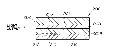
Referring to Fig. 6, description is made about a
laser diode eIement according to the second embodiment of
the present invention.
16
As illustrated in Fig. 6, the laser diode element
200 comprises a semiconductor block 201 having a front
facet 202, a rear facet 204 opposite to the front facet
202, a laser cavity 206 which is formed between the front
5 and the rear facets 202 and 204 and which has a
predetermined length L, an active layer 208 and a partial
grating 210 having regular corrugation which are formed
in the direction of the laser cavity 206 and which are
coupled to each other at a predetermined coupling
10 constant ~. The partial grating 210 is nearer to the
front facet 202 than to the rear facet 204 and is remote
from the front facet 202 to divide the direction of the
laser cavity into a short length side 212 and a long
length side 214 with the partial grating 210 interposed
15 between the short and the long length sides 212 and 214.
In this embodiment, the partial grating 210 is
remote from the front facet 202 and the rear facet 204
both of which are operable as cleaved surface.
Accordingly, laser diode elements, each of which is
20 cleaved and scribed from a wafer, become stable in their
characteristics. The laser diode elements having
sufficient characteristics can be manufactured in a good
yield.
Besides, the front facet and the rear facet may
25 be called a first end surface and a second end surface,
respectively.
Referring to Fig. 7, a laser diode element 220
according to the third embodiment of this invention has a
1j7
structure similar to that of the laser diode element 200
illustrated in Fig. 6 except for the followings.
In this embodiment, the partial grating 210' is
kept in contact with the front facet 202 to provide a
5 contact side 222 and a non-contact side 224 with the
partial grating 210' interposed therebetween and extended
from the contact side 222 towards the non-contact side
224. The coupling constant ~ is larger in the contact
side 222 than in the non-contact side 224. Namely, the
10 coupling constant ~ becomes small as a distance in the
direction becomes remote from the contact side 222.
Referring to Fig. 8, description is made about an
electrical field distribution in the direction of a laser
cavity in the laser diode element 220 illustrated in Fig.
15 7 in comparison with the conventional one.
As depicted by a continuous line A in Fig. 8, the
electrical field distribution in the laser diode element
220 becomes even or uniform in the direction of the laser
cavity compared with the conventional one of which the
20 distribution is depicted by a broken line B. A linearity
of I-L characteristics is therefore improved in this
embodiment. As a result, intermodulation distortion is
considerably decreased in this embodiment.
Referring to Fig. 9, a laser diode element 240
according to the fourth embodiment of this invention has
a structure similar to that of the laser diode element
200 illustrated in Fig. 6 except for the followings.
18
In this embodiment, the partial grating 210" is
kept in contact with the front facet 202 to provide a
contact side 222 and a non-contact side 224 with the
partial grating 210" interposed therebetween and extended
sfrom the contact side 222 towards the non-contact side
224. The regular corrugation of the grating has an
irregular portion 242 which is operable as a phase shift
portion.
Referring to Fig. 10, description is made about
lOan electrical field distribution in the direction of a
laser cavity in the laser diode element 240 illustrated
in Fig. 9 in comparison with the conventional one.
In Fig. 10, a continuous line C shows an
electrical field distribution in the laser diode element
15240 while a broken line D shows that of the conventional
laser diode element. As shown in Fig. 10, the continuous
line C has a peak in the portion corresponding to the
above-mentioned irregular or phase shift portion 242. As
a result, the electrical fleld distribution in the laser
20 diode element 240 becomes even or uniform along the laser
cavity compared with the conventional one.
Alternatively, a plurality of phase shift portions may be
formed in the grating. In this case, evenness or
uniformity of the distribution will be further improved.
Referring to Fig. 11, a laser diode element 260
according to the fifth embodiment of this invention has a
structure similar to that of the laser diode element 200
illustrated in Fig. 6 except for the followings.
1,9
In this embodiment, the partial grating 270 is
kept in contact with the front facet 202 to provide a
contact side 222 and a non-contact side 224 with the
partial grating 210 interposed therebetween and extended
sfrom the contact side 222 towards the non-contact side
224. The portion in which the partial grating 270 is
formed is operable as distributed Bragg reflector region
272.
A plurality of coating layers 274 are coated on
lOthe rear facet 204 which is opposite to the distributed
Bragg reflector region 272 to provide a high
reflectivity. Light output is generated from the front
facet 202 which is adjacent to the distributed Bragg
reflector region 272.
Referring to Fig. 12, description is made about a
relationship between a yield and coupling constant in the
laser diode element 260 illustrated in Fig. 11 in
comparison with the conventional one. In Fig. 12, the
yield is defined as a rate of numbers of the laser diode
20elements in which a value of the IMD3 is smaller than -80
dBc.
In Fig. 12, a continuous line E shows the yield
of the laser diode elements 260 while a broken line F
shows that of the conventional laser diode element.
As indicated in Fig. 12, the yield of the laser
diode elements 260 is stable even though the coupling
constant ~ is changed. In other words, the yield of the
laser diode elements 260 does not depend on the coupling
constant K. Consequently, it becomes unnecessary to
control the coupling constant ~ strictly.
Referring now to Figs. 13 through 15, description
will proceed to a method of manufacturing the
5 above-mentioned laser diode element according to the
second embodiment of the present invention.
As shown in Fig. 13(a), a substrate 300 of n-InP
is at first prepared in a known manner. A photoresist
302 is then coated on the substrate 300. The photoresist
302 is exposed by holographic lithography method to be
patterned with a period of 2025 angstroms.
Second, as illustrated in Fig. 13(b), the
substrate 300 and the patterned photoresist 302 are
closely exposed by the use of a mask 303 having a
predetermined mask pattern. In this event, an area in
which a grating should not be formed is selectively
permitted to be exposed. After being developed, a
predetermined pattern 304 is formed on the substrate 300
for partially making the grating, as illustrated in Fig.
13(c). The substrate 300 is etched to form a partial
grating 306 having a depth of 400 angstroms by using the
predetermined pattern 304 as an etching mask. In this
case, a coupling constant in the partial grating 306 is
40 cm 1.
Third, a light guiding layer 308 of n-InGaAsP is
grown on the partial grating 306 and the substrate 300 by
the aforesaid MOVPE method to have a thickness of 1000
angstroms. An active layer 310 of MQW structure is then
21
stacked on the light guiding layer 308 by the same method
to have a thickness of about 0.5 micron meters.
Thereafter, a clad layer 312 of p-InP is formed on the
active layer 310 by the same method to have a thickness
5 of approximately 0.5 micron meters.
Referring to Fig. 14, the active layer 310 of MQW
structure includes wells 320 and barriers 322. The wells
320 have a composition defined by a bandgap corresponding
to a wavelength of 1.40 micron meters. On the other
10 hand, the barriers 322 have a composition defined by a
bandgap corresponding to a wavelength of 1.13 micron
meters. Specifically, the wells 320 are equal in number
to ten. Each well is provided by a film having a
thickness of 62 angstroms while each barrier is also
15 provided by a film having a thickness of 100 angstroms.
The wells 320 and the barriers 322 are interposed on both
sides between SCH layers 324 and 326 each of which has a
composition defined by a bandgap corresponding to a
wavelength of 1.13 micron meters. Although it is not
20 shown in Fig. 14, the SCH layer 324 is adjacent to a
p-InP layer and has a thickness of 600 angstroms while
the SCH layer 326 is adjacent to a n-InP layer and has a
thickness of 300 angstroms.
After growth of these layers, a positive
25 photoresist (not shown) is coated on the layers.
Photolithography and etching are then carried out in a
known manner to form stripe-shaped grooves (not shown).
22
Thereafter, p-InP electric current blocking
layer, n-InP electric current blocking layer, p-InP clad
layer, and p-InGaAsP cap layer are formed one by one in a
known manner to form a double-channel planar buried
5 hetero (DC-PBH) structure.
Further, electrode layers are evaporated on both
surfaces of the DC-PBH structure. The DC-PBH structure
is cleaved at a predetermined portion.
As illustrated in Fig. 15, coating layers 330 are
10 coated on the rear facet 204 to provide a reflectivity of
75 ~ while the additional cladding layers 332 are coated
on the front facet 202 to provide a low reflectivity.
The coating layers 330 are composed of SiN. Thereafter,
the cleaved DC-PBH wafer is scribed or cut along the
15 width direction into a plurality of the laser diode
elements.
Under the circumstances, characteristics of each
of the laser diode elements have been investigated and
estimated. Consequently, it has been found out that the
20 laser diode element oscillates with a wavelength of 1.31
micron meters.
In order to estimate intermodulation distortion
characteristics of the laser diode element, the laser
diode element is assembled into a module so that IMD3 of
the laser diode element be measured. As a result, a
value of the above-mentioned IMD3 was -85 dBc on
conditions that an average light output power is 5 mW and
optical modulation index is 20 ~.
23 ~ ~ !a~ ~ ~ 2 ~
In order to investigate a merit of this
invention, a conventional laser diode element has been
fabricated as a comparative example. In this example, a
value of the IMD3 was -78 dBc on the same conditions.
Thus, it has been confirmed that the laser diode
element according to the embodiment of the present
invention has excellent intermodulation distortion
characteristics.
In this event, a yield, which is defined to be a
10 rate of numbers of the laser diode elements in which a
value of the above-mentioned IMD3 is smaller than -80
dBc, was 18 % in the laser diode element according to the
embodiment of the present invention while the yield was
about 12~ in the conventional laser diode elements.
Referring now to Figs. 16 through 18, description
will proceed to a method of manufacturing the above-
mentioned laser diode element according to the third
embodiment of the present invention. The method
according to the third embodiment has steps similar to
20 those of the above-mentioned second embodiment except for
the following points.
In this embodiment, a~ter a semiconductor
substrate 400 is prepared in a known manner, insulating
layers 402 of SiO2 are formed on the semiconductor
substrate 400, as shown in Fig. 16(a). A depth of the
partial grating 406 is made so that a coupling constant
in the partial grating 406 may be 30 cm 1. After the
partial grating 406 is formed, the insulating layers 402
24
of SiO2 as well as the photoresist 403 are removed from
the semiconductor substrate 400. Further, as illustrated
in Fig. 17, coating layers 430 are coated on the rear
facet 404 to provide a reflectivity of 90 % while the
5 additional coating layers 432 are coated on the front
facet 402 to provide a reflectivity of 1 %.
In this event, the above-described yield was 20%.
Besides, insulating layers 402 of SiO2 may alternatively
be replaced with insulating layers of Si3N4.
Another laser diode elements according to a
modification of the third embodiment have also been
fabricated.
As illustrated in Fig. 18, the laser diode
element has a partial grating 506 having a length of 60
15 micron meters. On the other hand, a length of the laser
cavity is 20 micron meters. Further, as illustrated in
Fig. 18, coating layers 530 are coated on the rear facet
504 to provide a reflectivity of 98 % while the
additional coating layers 532 are coated on the front
20 facet 502 to provide a reflectivity of 0.1 %.
In this event, the above-described yield was
about 22 %.
Referring now to Figs. 19 and 20, description
will proceed to a method of manufacturing the
above-mentioned laser diode element according to the
fourth embodiment of the present invention. The method
according to the fourth embodiment has steps similar to
those of the above-mentioned second embodiment except for
-~
the following points.
In this embodiment, after an InP substrate 600 iS
prepared in a known manner, a resist layer 602 for
electron beam exposure is coated on the InP substrate
5 600, as shown in Fig. l9(a). By the electron beam
exposure or lithography, a predetermined pattern 604 iS
formed on the substrate 600 for partially making the
grating, as illustrated in Fig. l9(b). The predetermined
pattern 604 iS enlarged to be shown in Fig. l9(c) merely
10 for the better understanding thereof. The pattern 604
has a period of 2048 angstroms. A ratio of exposed area
versus non-exposed area in each one period is changed
gradually from 1:1 to 1:10. The substrate 600 iS etched
to form a partial grating 606, as illustrated in Fig.
15 l9(d), by using the predetermined pattern 604 as an
etching mask.
Further, as illustrated in Fig. 20, coating
layers 630 are coated on the rear facet 604 to provide a
reflectivity of 75 % while the additional coating layers
20 632 are coated on the front facet 602 to provide a
reflectivity of 1 %. As illustrated in Fig. 20, the
partial grating 606 is kept in contact with the front
facet 602 and extends from the front facet 602 to have a
length of 100 micron meters. The coupling constant ~ is
25 larger in the contact side than in the non-contact side.
Namely, the coupling constant K is 70 cm 1 in the contact
side while 30 cm in the non-contact side.
26
A value of the above-mentioned IMD3 of the laser
diode element has also been measured. As a result, the
value of the IMD3 was -85 dBc.
Referring to Fig. 21, description will proceed to
5 a laser diode element according to the fifth embodiment
of the present invention. The fifth embodiment has a
structure similar to that of the above-mentioned second
embodiment except for the following points.
In this embodiment, as illustrated in Fig. 21,
10 the partial grating 706 extends from the front facet
702 to have a length of 100 micron meters, like the
laser diode element illustrated in Fig. 20, but has
the coupling constant ~ of 50 cm 1 uniformly from
the contact side to the non-contact side. The partial
15 grating 706 has, however, an irregular portion 710
which is operable as a ~/4 phase shift portion. The
irregular portion 710 is positioned where the partial
grating 706 extends from the front facet 702 by 70 micron
meters.
A value of the above-mentioned IMD3 of this laser
diode element has also been measured. As a result, the
value of the IMD3 was -82 dBc.
Further, an intensity ratio of a main mode
oscillation and a sub-mode oscillation is also measured.
25 The intensity ratio was 35 dBc in the embodiment,
although 38 dBc in the conventional laser diode element.
Furthermore, the similar effects have been
achieved in another fabricated laser diode elements, in
27 ~ ~ ~ 7~
case that the grating includes a phase shift portion
falling within a range between ~/8 and ~/2.
Thus, characteristics of single mode oscillation
is improved in the laser diode element according to this
5 embodiment.
Referring to Fig. 22, description will proceed to
a laser diode element according to the sixth embodiment
of the present invention.
In this embodiment, as illustrated in Fig. 22,
the laser diode element has the partial grating 806
extends from the front facet 802 to have a length of 100
micron meters to make a distributed Bragg reflector
region 810.
Further, as illustrated in Fig. 22, coating
layers 830 are coated on the rear facet 804 to provide a
reflectivity of 75 % while the additional coating layers
832 are coated on the front facet 802 to provide a
reflectivity of 1 %. The partial grating 806 has the
coupling constant K of 50 cm 1 uniformly from the contact
side to the non-contact side.
A value of the above-mentioned IMD3 of the laser
diode element has also been measured. As a result, the
value of the IMD3 was -83 dBc. In addition, the
above-described yield was about 25 %.
Moreover, the similar effects have been achieved
in another fabricated laser diode elements, in case that
a reflectivity of coating layers coated on the rear facet
falls within a range between 40 % and 98 %.
v~
28
While this invention has thus far been described
in conjunction with several embodiments thereof, it will
now be readily possible for one skilled in the art to put
this invention into effect in various other manners. For
example, the active layer is not restricted to have the
above-mentioned MQW structure. The active layer may also
have a bulk structure.