Note: Descriptions are shown in the official language in which they were submitted.
SPECIFICATION
TITLE OF THE INVENTION
NON-REDUCING DIELECTRIC CERAMIC COMPOSITION
FIELD OF THE INVENTION
The present invention relates to a non-reducing
dielectric ceramic composition, and in particular to a
non-reducing dielectric ceramic composition to be used in
multilayer ceramic capacitor, in which a base metal such as
nickel is used as internal electrode.
BACKGROUND OF THE INVENTION
with rapid propagation of various types of electronic
devices, there is a tendency that these devices are
increasingly produced in compact and lightweight design.
In particular, this tendency toward compact and lightweight
design is more remarkable in the electronic devices of
portable type to be used in camera-integrated video tape
recorder, portable telephone set, note-book personal
computer, palm-top computer, etc.
In such tendency toward compact and lightweight
electronic products, the component parts for these devices
are also increasingly produced in compact and lightweight
design. The means to mount the electronic components are
-1-
also changing from the technique for inserting and soldering
pins, i.e. electronic parts, to be used in through-hole on
conventional type printed board to surface mounting
technology (SMT), i.e. the technique for mounting and
soldering electronic parts on land of electro-conductive
pattern on printed board.
The electronic parts used in this SMT are generally
called surface mounting devices (SMD). Not only semi-
conductor components, but also capacitor, resistor,
inductor, filter, etc. are included in them. Among them,
small components such as capacitor and resistor are called
chip components. The most representative of them is multi-
layer ceramic capacitor.
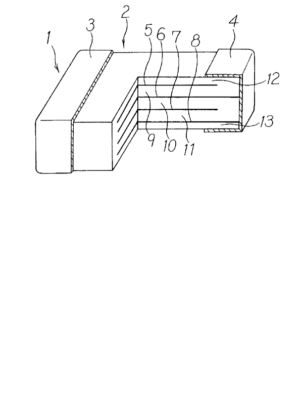
Fig. 1 shows a partially cutaway perspective view
showing structure of a multilayer ceramic capacitor.
The multilayer ceramic capacitor 1 is in form of
rectangular parallelopiped, and terminal electrodes 3 and 4
are mounted on a pair of opposed surfaces of multilayer
ceramic capacitor body 1, which is in form of rectangular
parallelopiped.
In the multilayer ceramic capacitor main unit 2, four
internal electrodes 5, 6, 7 and 8 are formed among laminated
BaTi03 dielectric layers 9, 10 and 11, and dielectric
-2-
~~~3~6~
material layers 12 and 13 made of dielectric material are
laminated on upper surface of the internal electrode and
lower surface of the internal electrode 8.
Every other of the internal electrodes 5, 6, 7 and 8
are connected to terminal electrodes. That is, the internal
electrodes 6 and 8 are connected to a terminal electrode 4,
and the internal electrodes 5 and 7 are connected to another
terminal electrode 3. As a result, a capacitor is formed,
which is connected in parallel between the internal
electrodes 5 and 6, between the internal electrodes 6 and 7,
and between the internal electrodes 7 and 8.
Each of the terminal electrodes 3 and 4 comprises a
conductive layer, on which conductive paste containing glass
frit is coated or printed and baked, and a plated layer
coated on it or a metal cap press-fitted on it.
To manufacture multilayer ceramic capacitor, electrode
paste to serve as an internal electrode is printedon a diele
ctric ceramic composition sheet, a plurality of such sheets
are laminated and thermally pressed, the laminated product
thus prepared is sintered in the air and a terminal
electrode is mounted on it.
In this manufacturing method, the electrode paste to
serve as the internal electrode of the capacitor and the
-3-
~1~3a6~
dielectric ceramic composition are fired at the same time.
For this reason, the material to be used as the internal
electrode must have such property that the electrode is
formed at the sintering temperature of the dielectric
ceramic composition and there occurs no oxidation or no
reaction with the dielectric ceramic composition When heated
in the air.
As the material to meet the above requirements,
noble metal such as platinum, palladium, etc. have been used
in the past. However, these noble metals are very expensive
and constitute major cause for the high cost of the multilay
er ceramic capacitors.
In this connection, attempts have been made to use base
metal such as nickel as internal electrode, while nickel is
oxidized when it is fired in oxidizing atmosphere and also
reacts with the dielectric ceramic composition. This
hinders the formation of electrode.
A method to fire nickel in non-oxidative atmosphere to
prevent oxidation is disclosed in the specification of U.S.
Patent No. 4, 241, 378, whi le, in this method, dielectric
ceramic composition is reduced and specific resistance is
extremely lowered. Thus, it is not suitable for the
practical use as capacitor.
-4-
X113060
As a dielectric ceramic composition having satisfactory
dielectric property such as dielectric constant (relative
permitivity), BaTi03 dielectric ceramic composition
containing CaZr02, MnO, etc. is disclosed in Japanese Patent
Laid-Open Publication 62-2408, whereas this dielectric
ceramic composition is fired in non-oxidizing atmosphere
when it is reduced and has shorter life time.
The multilayer ceramic capacitor is manufactured
through the following processes.
(1) Raw materials are weighed and blended so that
composition after firing complies with the pre-
determined blending ratio.
(2) bet mixing and pulverizing are performed.
(3) Dehydration and drying are performed.
(4) Adequate quantity of organic binder is added, and it
is mixed and turned to enameled.
(5) This is coated on film by doctor blade method to form
dielectric ceramic composition sheet.
(6) On the dielectric ceramic composition sheet thus
prepared, nickel paste to serve as a material for
internal electrode is formed by printing.
(7) The product is laminated and thermally pressed to
obtain a multilayer product.
- 5 -
~~~.a~b~
(8) The product is cut into a predetermined shape.
(9) Binder removal processing is performed.
(10) ~Yhile controlling oxygen partial pressure, the product
i s f i red.
(11) Re-oxidation is performed in neutral atmosphere.
(12) Terminal electrode is mounted.
As a non-reducing dielectric ceramic composition having
longer life time, a dielectric ceramic composition contain-
i ng ~BaA, Ca c , -A, }S i 03 (where 0 s A~ 1 ) (here i naf ter referred
as "BCG") as an additive to BaTi03, MnO, and Y203 is dis-
closed in Japanese Patent Application 3-18261. However, in
the multilayer ceramic capacitor produced using this di-
electric ceramic composition, capacitance is varied due to
temperature change.
In addition to the above, non-reducing dielectric
ceramic composition is described in Japanese Patent Laid-
Open Publications 61-248304 and 57-71866, U.S. Patent
4,115,493, "Dielectric Materials for Base-Metal Multilayer
Ceramic Capacitors" (Proceedings of the Electronics Division
Fall Meeting, the American Ceramic Society, October 13-16,
1985) by Y. SAKABE, T. TAKAG I , and K. OAK I N0.
-6-
SUMMARY OF THE INVENTION
It is an object of the present invention to provide a
non-reducing dielectric ceramic composition suitable for
producing a multilayer ceramic capacitor, in Which decrease
of specific resistance and shortening of service life do
not occur due to reduction of the dielectric ceramic
composition even When nickel to be used for internal
electrode is fired in neutral or reducing atmosphere to
prevent oxidation, in which capacitance does not vary
extensively due to temperature change.
To attain the above object, the non-reducing dielectric
ceramic composition comprises 86.32 to 97.64 mots of
BaTi03, 0.01 to 10.00 cools of Y203, 0.01 to 10.00 mots of
MgO, and 0.001 to 0.200 cools of V205.
?1~3~~~
BRIEF DESCRIPTION OF THE DRAI~INGS
Fig. 1 shows structure of a multilayer ceramic
capacitor; and
Fig. 2 is a flow chart~showing manufacturing process
of the non-reducing dielectric ceramic composition.
DETAILED DESCRIPTION OF THE PREFERRED EMBODIMENTS
In the following, description will be given on the
features of the present invention in connection with
embodiments.
A flow chart showing manufacturing process of the
non-reducing dielectric ceramic composition of the present
invention is given in Fig. 2.
(1) BaTi03, Y203, MgO, V205, MnO, Cr20s, Co20s, etc.
are weighed and blended to have the composition after
firing as shown in Table 1 and 'Table 2.
;'1.~.3fl6~
Table 1
Composition Fir'g
(mold) Temp
.
No. BCG* X Y Z XYZ
Total T
BaTi03Y203 MgO V205 2
A Q'ty Mn0 Cr203Co203Q'ty (C)
1 97.690 0.02 0.0010.581.95 0.050.29 -- 0.34 1400
2 97.540.20 0.02 0 0.581.95 -- 0.29 -- 0.29 1380
3 96.880.58 0.02 0 0.581.94 0.290.29 -- 0.58 1380
4 97.040.58 0 0.0050.581.94 0.150.29 -- 0.44 1380
96.250.58 0.96 0.0050.581.92 0.29-- -- 0.29 1340
6 96.890.58 0.01 0.30 0.581.94 0.290.29 -- 0.58 1340
7 96.610.58 0.01 1.00 0.581.93 0.290.58 -- 0.87 1340
8 96.390.58 0.96 0.0050.581.93 0.14-- -- 0.14 1300
9 92.680.58 4.63 0.0020.581.85 0.28-- -- 0.28 1300
95.860.01 1.92 0.0050.581.92 0.29-- -- 0.29 1380
11 87.430.53 10.000.0010.581.77 0.27-- -- 0.27 1300
12 85.950.53 11.500 0.581.76 0.26-- -- 0.26 1300
13 96.480.58 0.96 0.0050.581.93 0.05-- -- 0.05 1340
14 96.670.29 0.97 0.0050.581.93 0.14-- -- 0.14 1340
97.280.58 0 0.0010.581.95 -- 0.19 -- 0.19 1320
16 97.450.58 0.02 0 0.581.95 -- -- -- 0 1320
17 96.510.58 0.97 0.0050.581.93 0.01-- -- 0.01 1320
18 95.470.57 1.91 0.0020.581.91 0.14-- -- 0.14 1340
19 92.800.56 4.64 0.0020.581.86 0.14-- -- 0.14 1340
95.470.57 1.91 0.0500.581.91 0.14-- -- 0.14 1340
21 95.420.57 1.91 0.0010.581.91 -- 0.19 -- 0.19 1380
22 97.240.58 0.05 0.0500.581.94 -- 0.19 -- 0.19 1380
23 95.420.57 1.91 0.0300.581.91 -- 0.19 -- 0.19 1360
*BCG: {BaA, Ca c, -,., }S i03
- 10 -
a1~.3~60
Table 2
Composition Fir'g
(mol%)
_
_. Temp.
No. B Y 0 0 BCG~ X Y Z XYZ
Ti0 0 M V
a 3 g 2 TotalT2
3 2 5 A Q'ty Mn0 Cr203Co20s Q'ty (C)
24 95.420.57 1.91 0.003 0.581.91 -- 0.19 -- 0.19 1360
25 95.420.57 1.91 0.010 0.581.91 -- 0.19 -- 0.19 1360
26 95.480.57 1.91 0.240 0.581.90 0.14-- -- 0.14 1360
27 96.530.39 0.96 0.190 0.581.93 -- 0.19 -- 0.19 1360
28 97.260.58 0.01 0.002 0.581.95 -- 0.20 -- 0.20 1320
29 95.050.95 0.90 0.002 0.581.91 -- 0.19 -- 0.19 1360
30 91.584.58 1.83 0.002 0.581.83 -- 0.18 -- 0.18 1340
31 86.3210.00 1.75 0.005 0.581.75 -- 0.18 -- 0.18 1340
32 85.3911.00 1.72 0.001 0.581.72 -- 0.17 -- 0.17 1340
33 98.140.59 0.98 0.001 0.580 0.29-- -- 0.29 1380
34 97.640.59 0.98 0.001 0.580.50 0.29-- -- 0.29 1320
35 93.540.56 0.94 0.001 0.584.68 0.28-- -- 0.28 1340
36 88.300.54 0.89 0.001 0.5810.000.27-- -- 0.27 1300
37 85.790.53 0.88 0.001 0.5812.540.26-- -- 0.26 1300
38 96.400.58 0.10 0.001 0.581.93 0.310.68 -- 1.00 1360
39 92.510.74 0.09 0.001 0.585.55 0.650.46 -- 1.11 1360
40 96.110.58 0.96 0.001 0.581.92 -- 0.29 0.14 0.43 1360
41 96.110.58 0.96 0.001 0.581.92 0.14-- 0.29 0.43 1320
42 97.190.58 0.05 0.001 0.581.94 0.05-- 0.19 0.24 1360
43 91. 4. 1. 0. 1. 1. -- 0, -- -- 1390
85 58 83 002 0 83 18
44 91. 4. 1. 0. 0. 1, -- 0. -- -- 1360
58 58 83 002 7 83 18
45 91.584.58 1.83 0.002 0.3 1.83 -- 0.18 -- -- 1340
46 91.584.58 1.83 0.002 0 1.83 -- 0.18 -- -- 1340
*BCG: {Ba~, Ca ~ , -~> } S i 03
- 11 -
~1~.3U6U
As the starting materials, BaTi03 is used, which is
obtained by blending Ba0 and Ti02 at molar ratio of 1 : 1
and by chemical reaction at 900°C to 1200°C. As this BaTi03,
powder (50 ~ of the particles being in particle size 0.8 a
to 1.2 a ) prepared by solution method, or BaTi03 obtained
from BaC03 and Ti02 pulverized by atomizer to particle size
of about 1 ,u m may be used.
(2) Wet mixing and pulverizing are performed.
(3) Dehydration and drying are performed.
(4) Adequate quantity of organic binder is added and mixed
to turn it to enameled.
(5) The material thus prepared is coated on film in
thickness of 20 a m by doctor blade method, and
dielectric ceramic composition sheet is prepared.
(6) Nickel paste used as the material for internal
electrode is printed on the dielectric ceramic
composition sheet.
(7) This is laminated in five layers and thermally pressed
to prepare a multilayer product.
(8) The multilayer product thus prepared is cut into 3216
shape, i. e. in size of 3. 2 mm (length) x 1. 6 mm.
(9) Stabilizing at 250°C to 300°C, binder removal
processing is performed for 10 hours.
(10) Oxygen partial pressure is controlled to 7 x 10⁻⁹ to
9 x 10-'3 atm, and stabilizing at firing temperature
- 12 -
~'1~ 3~6~
T2 - 1, 200°C to l, 300°C, it is fired for 2 hours.
(11) Stabilizing at 700°C to 1,200°C in neutral atmosphere,
re-oxidation is performed for 9 hours.
(12) A terminal electrode of indium-gallium (In-Ga) alloy
is mounted on it.
The capacitor thus prepared has capacitance of 20 pF
in each layer, being 100 pF in total.
On the specimen capacitors prepared as above,
electrical properties such as dielectric constant E s,
dielectric loss tan ~, insulation resistance IR (S~),
temperature characteristic of capacitance T~C (~), and
life time ,u (hour) were determined. The results are shown
in Tables 3 and 4.
~~ ~3oso
Table 3
TC(%)
No. s tan IR a
s 8 (S~) -55C -25C 85C 125C (hour)
1 Difficult
to
sinter
2 33902. 5 x -13. - 8. - - 3
6 10' 2 0 8. 1.
5 0
3 38002. 8 x - - 4. 0 6. 4
2 10' 5. 0 0
0
4 39202. 2 x -16. -12. - - 9
8 10' 8 7 7. 1.
0 3
5 36001. 5 x -13. - 7. - 2. 100
9 10" 2 8 5. 0
4
6 21002.3 5x10⁹ -12.0-7.5 -5.4 -3.1 7
7 14005.4 8x10' -10.9-6.0 -1.0 2.8 3
8 31002.0 2x10" -14.2-9.0 -4.0 -1.0 90
9 29001. 3 x - - 5. - - 34
8 10' 8. 3 8. 4.
' 0 5 0
10 32501.8 3x10" -8.4 -5.8 -6.4 -1.7 31
11 25601. 1 x - - 5. - - 37
6 10" 7. 3 9. 8.
6 6 7
12 18101. 1 x - - 5. -11. -13. 0
4 10" 8. 3 4 4
9
13 28202. 2 x -15. - 9. - 2. 36
2 10" 0 8 1. 0
l
14 31802. 2 x -14. - 8. 3. 0 29
6 10" 8 7 7
15 37905. 2 x -17. -11. - 2. 45
9 10" 8 9 1. 0
0
16 Turned
to
semiconductor
state
17 30001. 2 x -14. - 9. 0 12. 39
8 10' 8 8 5
18 31801.8 3x10" -8.6 -6.2 -5.1 1.0 60
19 30502. 1 x -10. - 6. - - 48
2 10" 2 1 7. 3.
8 7
20 24801. 2 x -11. - 8. - 4. 200
5 10" 7 4 4. 6
4
21 32102. 2 x - - 5.1 - 0 25
0 10' 7. 6.
' 4 3
22 28002. 3 x - - 6. - 1. 150
2 10' 8. 1 6. 0
3 4
23 30002. 1 x - - 3. - - 110
2 10' 5. 3 7. 3.
' 7 8 8
- 14 -
?1~~3~~0
Table 4
TC(~)
No. s tan IR a
s ~ (S2) -55C -25C 85C 125C (hour)
24 31802.1 2 x - - 5. - 4. 52
10' 8. 0 5. 0
' 5 0
25 32602. 1 x - - 5. - 2. 100
1 10" 7. 5 6. 0
9 2
26 24801. 8 x -10. - 7. - 0 6
8 109 6 9 6.1
27 31001. 3 x - - 6. - - 200
9 10' 8. 2 7. 3.
5 5 2
28 30103. 2 x -15. - 9. - - 33
0 10" 0 8 2. 3.
4 4
29 31502.0 3x10" -8.5 -5.9 -6.3 -2.0 28
30 29501. 2 x -10. - 8. - - 25
9 10" 5 7 4. 5.
4 0
31 26501. 3 x - - 5. - - 46
6 10' 7. 4 3. 9.
' 5 8 0
32 Turned
to
semiconductor
state
33 43305. 1 x -35. -20. -11. -18. 8
2 10" 2 0 3 5
34 32101. 3 x -15. -10. 0 7. 28
7 10" 0 0 5
35 28801. 1 x -13. - 6.1 - - 40
9 10" 0 6. 4.
5 0
36 26101.6 2x10" -8.9 -7.0 -6.0 -5.5 38
37 19101.4 3x10" -5.0 -4.0 -3.0 -5.0 9
38 26801. 2 x - - 3. - - 85
2 10' 6. 5 2. 4.
9 5 8
39 13801. 4 x - - 2. - - 7
0 109 4. 6 8. 9.
6 0 0
40 30801. 1 x -13. -10. - - 35
9 10" 8 0 9. 8.
0 5
41 29802. 7 x -11. - 7. - - 36
0 10' 8 4 4. 1.
6 9
42 38503. 4 x -14. - 8. - - 40
0 10' 9 9 7. 4.
8 0
43 31602.2 2x10" -11.5-9.0 -2.0 -7.0 35
44 31202.0 1x10" -10.6-8.4 -4.9 -5.0 30
45 30002. 3 x -14. -10. - - 25
0 10" 5 0 7. 8.
0 5
46 28501. 3 x -14. - 9. - - 26
4 10' 9 8 5. 9.
' 0 8
- 15 -
1_1_3060
Here, dielectric constant s s and dielectric loss tan 8
are the values at 20°C and frequency of 1 kHz. The insula-
tion resistance IR is measured at 20°C after voltage of 50 V
has been applied for 30 seconds, and temperature character-
istic of capacitance T~C is temperature characteristic to
capacitance at 20°C of the capacitance at each temperature,
and life time ,u is accelerated life time, applying voltage
of 200 V at 200°C.
In the evaluation of the above measurements, the values
were considered as satisfactory if dielectric constant E s
is 2, 500 or more, dielectric loss tan ~ is 3. 0 or less,
insulation resistance IR is 10'°S2 or more, temperature
characteristic of capacitance T~C is within ~ 15%, and life
time a is 10 hours or more. If the values do not comply
with these criteria, the product was considered as defective.
The product which was difficult to sinter or was
turned to semiconductor state was considered as defective
because such is not suitable for the use as capacitor.
As the result of the evaluation in accordance with the
above cr i ter i a, the spec imens Nos. 5, 8, 9, 10, 1 l, 13, 14,
17, 18, 19, 21, 22, 23, 24, 25, 27, 28, 29, 30, 31, 34, 35,
36, 38, 40, 41, 42, 43, 44, 45, and 46 were ~ udged as
satisfactory, and the specimens Nos. 1, 2, 3, 4, 6, 7, 12,
- 16 -
~1~.3060
15, 16, .20, 26, 32, 33, 37, and 39 were j udged as
def ec t i ve.
Based on the results of the above judgment, the
composition range is defined as follows:
In case Y203 is less than 0.01 mol% (specimen No. 1),
it is difficult to sinter even when the firing temperature
(T2) - 1,400°C and is not suitable for practicaluse. In
case it exceeds 10.0 mol% (specimen No. 32), the composition
is reduced and is turned to semiconductor state.Thus, it
does not act as a dielectric substance.
Therefore, to obtain satisfactory results, Y203 must
be w i th i n the range of 0. O 1 to 10. 0 coo I %.
In case Mg0 is contained by less than 0.01 mol%
(specimens Nos. 4 and 15), temperature characteristic of
capacitance T~C is aggravated to more than ~ 15%, and
dielectric loss tan ~ may be as high as 5.9. In case it
exceeds 10.0 cools (specimen No. 12), accelerated life time
is extremely aggravated.
Therefore, to obtain satisfactory results, Mg0 must be
within the range of 0.01 to 10.0 cool%.
VYhen V203 is added by more than 0.001 mol% (all speci-
mens except Nos. 2, 3, 12 and 16), accelerated life time is
- 17 -
X11_3060
extensively improved. In case it is added by more than 0.20
mol% (specimens Nos. 6, 7 and 26), dielectric constant s s
is 2500 or less and insulation resistance is 1 x 10'°S2 or
less, and the product is not suitable for practical use.
Therefore, to obtain satisfactory results, V205 must
be w i th i n the range of 0. 001 to 0. 20 mo I %.
I n case {Baa" Ca c , -A, } S i 03 (Where 0 s A s 1) i s added by
less than 0.5 mol% (specimen No. 33) as the additive BCG,
temperature characteristic of capacitance is more than
~ 15%. In case it exceeds lOmol % (specimen No. 37), s s is
2500 or less.
Therefore, to obtain satisfactory results, the additive
BCG must be within 0.5 to 10 mol %.
In case total quantity of Mn0~Cr203~Co203 is less than
0.01 mol % (specimen No. 16), the composition is turned to
semiconductor state. In case it exceeds 1.0 mol % (specimen
No. 39), insulation resistance is 1 x 10'°S2 or less.
Therefore, to obtain satisfactory results, total
quantity of Mn0~Cr203~Co203 must be within the range of 0.01
to 1. 0 mo 1 %.
By the non-reducing dielectric ceramic composition
according to the present invention within composition range
- I8 -
~1~ 3064
as described above, it is possible to obtain multilayer
ceramic capacitor, in which decrease of specific resistance
and shortening of service life due to reduction of
dielectric ceramic composition, even when nickel used as
internal electrode is fired in neutral or reducing
atmosphere to prevent oxidation and capacitance does not
vary extensively due to temperature change.
- 19 -