Note: Descriptions are shown in the official language in which they were submitted.
2113135
TITLE OF IN'JENTION
CARRIER PHASE ESTIMATION SYSTEM USING FILTER
BACKGROUND OF THE INVENTION
i) Field of the Invention:
The present invention relates to a carrier phase
estimation apparatus for estimating a carrier phase of a
PSK-modulated received signal in a radio communical.~ion field
by a movable body such as a mobi7_e satellite communication,
and more particularly to a carrier phase estimation
apparatus constituted by digital circuits, which is capable
of following up a received carrier phase variation caused by
fading.
ii) Description of the Related Arts:
Fig. 7 illustrates a conventional digital carrier phase
estimation apparatus for estimating a carrier phase of a
PSK- (phase shift keying-) modulated received signal, as
disclosed in "Nonlinear Estimation of PSK-Modulated Carrier
Phase with Application to Burst Digital Transmission" by
Andrew J. Viterbi and Audrey M. Miterbi, IEEE Transactions
of Information Theory, Vol. IT-29, No. 4, pp. 543-551, July,
1983. As shown in Fig. 7, a base band converter 1 takes a
received IF signal 3 as input and outputs an in-phase
component In and an quadrature component Qn of a digital
-1-
_ 21~.313~
base band signal. A phase estima~.tor 2 receives the in-phase
component In and the quadrature component Qn output from the
base band converter 1 and estimates a received carrier phase
8 every symbol and outputs a carrier phase 8 estimated every
symbol (herein-after referred to as an estimated carrier
phase On; n = 0, 1, 3, ...). The base band converter 1
includes a pair of multipliers 4 and 5 for receiving the
received IF signal 3 and the output signals of the
multipliers 4 and 5 are supplied to a pair of LPFs (low pass
filters) 8 and 9, respectively. The output signals of the
LPFs 8 and 9 are fed to a pair of A/D (analog-digital)
converters 10 and 11, respectively) and the A/D converters
and 11 convert the output signals into digital signals to
obtain the in-phase component In and the quadrature
component Qn of the digital base band signal. The base band
converter 1 further includes a carrier oscillator 6 and a
90° phase shifter 7. Because of the carrier oscillator 6
and the 90° phase shifter 7, carrier signals having 90°
different phases are supplied to the multipliers 4 and 5.
The phase estimator 2 includes a non-linear circuit 12
which receives the in-phase component In and the quadrature
component Qn of the digital base band signal and executes a
non-linear operation. The in-phase and quadrature
components In' and Qn' output by the non-linear circuit 12
are input to a pair of filters 13 and 14 and the output
signals of the filters 13 and 14 are sent to a coordinate
transformer 18 which transforms tlhe output signals into a
-2-
2113135
carrier phase On. The filters 13 and 14 have the same
construction and each filter 13 or 14 is constituted by N (N
is a positive integer) stages of shift registers 15, an
adder 16 and a divider 17.
Next) an operation of the conventional carrier phase
estimation apparatus shown in Fif. 7 will be described in
detail.
First the received IF signal 3 is converted into the
in-phase component In and the qua.drature component Qn of the
digital base band signal by the base band converter 1. In
the base band converter 1, the received IF signal 3 is
branched off in two directions) that is) one branch is input
to the multiplier 4 and the other branch is input t.o the
multiplier 5. The carrier oscillator 6 outputs a carrier
having the same frequency as that of the received IF signal
3 and the output signal of the carrier oscillator 6 is
supplied to the multiplier 4. As a result, in the
multiplier 4, a product of the received IF signal 3 and the
output signal of the carrier oscillator 6 is obtained. On
the other hand, the output signal of the carrier oscillator
6 is input to the multiplier 5 via the 90' phase shifter 7.
As a result, in the multiplier 5, a product of the received
IF signal 3 and the output signal of the 90° phase shifter 7
is obtained.
The output signal of the multiplier 4 is input: to the
LPF 8 and the LPF 8 removes unnecessary harmonic components
from the output signal of the multiplier 4 and outputs the
-3-
211313
in-phase component of the base band signal. The output
signal of the multiplier 5 is input to the LPF 9 and the LPF
9 removes unnecessary harmonic components from the output
signal of the multiplier 5 and outputs the quadrature
component of the base band signal.. The in-phase component
of the base band signal output from the LPF 8 is input to
the A/D converter 10 in which the: in-phase component is
sampled by a clock (not shown) of a symbol period and is
converted into the in-phase component In of the digital base
band signal, and the A/D converter 10 outputs the in-phase
component In of the digital base band signal. The
quadrature component of the base band signal output from the
LPF 9 is input to the A/D converter 11 in which the
quadrature component is sampled by a clock (not shown) of a
symbol period and is converted into the quadrature component
Qn of the digital base band signal. and the A/D converter 11
outputs the quadrature component Q,n of the digital base band
signal.
In this case, for simplifying and better understanding
of the explanation) it is assumed that the received IF
signal 3 is a BPSK- (binary PSK-) modulated signal with no
noise and a phase difference between the received IF signal
3 and the output signal of the carrier oscillator 6 is, for
example) 22.5°. For example) when a data series is "10110",
the in-phase component In and the quadrature component Qn of
the digital base band signal are represented by formulas (1)
represented hereinbelow. And these components are shown by
-4-
211313
(a) to (e) in Fig. 8.
In = A~d"~cos8n
Qn = A~d"~sin9n ........................ (1)
In the formulas (1), A represents an amplitude and do
represents a value of either +1 or -1 corresponding to "1"
and "0". In this case, the value: of 22.5° is a value of the
carrier phase to be estimated by the carrier phase
estimation apparatus.
Next, the in-phase component In and the quadrature
component Qn of the digital base band signal are input to
the phase estimator 2. In the phase estimator 2, first, the
components In and Qn are input to the non-linear circuit 12
which executes a non-linear operation represented by formula
(2) shown below against the in-phase component In and the
quadrature component Qn.
In' - p~cosm8n
Qn' - p~sinm9n ......................... (2)
In the formulas (2), m represents a value corresponding to
an m-phase PSK signal. For instance, in the case of the
BPSK signal, because of binary phase, m =2 and in t;he case
of a QPSK signal, m = 4. Also) p possesses a function for
changing the estima-tion characteristics of the carrier
phase by its value. In the aforementioned document:, it is
disclosed that good results can be obtained when p = 1 or p
- In2 + Qn2. In this case, for simplifying the explanation,
assuming that p = 1) when the received IF signal 3 is the
BPSK-modulated signal, the output signals In' and Qn' of the
-5-
2~13I35
non-linear circuit 12 are shown by formulas (3) as follows.
In' - cos26n
Qn' - sin28n ............................ (3)
Fig. 9 illustrates the signals In' and Qn' which are
obtained by modifying the in-phase component In and the
quadrature component Qn of the digital base band signal
shown in Fig. 8 by the non-linear circuit 12. In this case,
261 - 282 - 263 - 26~ = 285 - 45° and the data modulating
component is removed. That is, the non-linear circuit 12
removes the data modulating component of the m-phase PSK
signal.
Fig. 10 shows the above-described converted values In'
and Qn' as a list. As shown in Fig. 10, in this case, the
in-phase components of the digital base band signal become
In' - cos26n = cos45° - 0.707 and the quadrature components
of the same become Qn' - sin26n = sin45° - 0.707.
The in-phase components In' ;end the quadrature
components Qn' of the digital base band signals, modified
and output by the non-linear circuit 12, are supplied to the
respective filters 13 and 14 in which the noise included in
the components In' and Qn' is reduced.
In the filter 13) the in-phase components In' of the
digital base band signal is input to the shift registers 15.
The N number of components In' input in the shift registers
15 are added to each other in the adder 16. At this time,
the value of the symbol number n of the filter output signal
Xn is equal to the symbol number n of the component In'
-6-
2113135
input in the central stage of the shift registers 15. For
example) as shown in Fig. 10, in the state that 5 components
In' of n = 1 to 5 are input in the shift registers 15, the
component I3' is input in the central stage of the shift
registers 15 and thus the filter output signal Xn is X3.
That is, the filter 13 performs the operation for taking an
average by using the (N-1)/2 numbers of the components In'
aligned in the front and rear sides of the central component
In' input in the central stage of the shift registers 15 to
reduce the noise.
The filter 14 has the same construction as the filter
13 and operates the input quadrature components q.n' of the
digital base band signals in the same manner as the filter
13 to output a filter output signal Yn.
In the example shown in Fig. 10,
X3 - (0.707 + 0.707 + 0.707 + 0.707 + 0.707)/5
- 0.707, and
Y3 - (0.707 + 0.707 + 0.707 + 0.707 + 0.707)/5
- 0.707.
Next, the filter output signals Xn and Yn are input to
the coordinate transformer 18. The coordinate transformer
18 executes an operation shown in formula (4) and outputs
the estimated carrier phase On.
On = (1/m)~tan-1(Yn/Xn) .".............. (4)
In formula (4)) m represents the value corresponding to the
m-phase PSK signal, and in the case of the BPSK signal) m =
2. Also, in the case of the QPSK signal) m = 4. In the
_7_
~113I3~
example shown in Fig. 10) it is calculated as follows.
On = (1/2)~tan-1(Y3/X3) - 22.5' ........ (5)
In this case, the true estimation value of the carrier phase
0 = 22.5' is estimated. The estimation operation of the
above-described carrier phase is carried out against each
symbol (n = ..., -2, -1, 0, 1, 2, 3, ...).
In the conventional embodiment described above, since
the case that no noise is attached to the received IF signal
3 is described, the carrier phase can be estimated without
any error. However, in case that noise is contained in the
received IF signals 3, in order to remove the influence of
the noise, a required larger number of filter stages are
designed.
In Fig. 11) there is shown a conventional data
demodulation apparatus using the ~~arrier phase estimated in
the above-described carrier phase estimation apparatus.
As shown in Fig. 11, a sine wave generator 19 inputs
the estimated carrier phase On ou-tput from the phase
estimator 2 and outputs cosine and sine signals of cosOn and
sinOn. A pair of multipliers 20 and 21 multiply the output
signals cosOn and sinOn of the sine wave generator 19 by the
in-phase component In and the quadrature component Qn of the
digital base band signal, respect_Lvely, to output signals tn
and u~, respectively. The output signals tn and un of the
multipliers 20 and 21 are added to each other in an adder
22. The added value of the adder 22 is supplied to a
discriminator 23 and the discriminator 23 discriminates the
_g_
2113135
input data and outputs demodulated data.
The in-phase component In and the quadrature component
Qn of the digital base band signal are represented by
formulas (1) and hence the signals t" and u" output from the
multipliers 20 and 21 are represented in formulas (6) as
follows.
t" = A~d"~cosAn~cosOn
u" = A~d"~sin6n~sinOn ...........,.,,,,, (g)
When the carrier phase estimation apparatus correctly
estimates the carrier phase, On = 8n and the formulas (6)
can be rewritten to formulas (7) as follows.
t" - A~d"~cos29n
u" = A~d~~sin29n ....................... (7)
As a result, the output signal of the adder 22 is t" + u" _
A~d". Hence, the discriminator 2.3 discriminates the
positive and the negative of the output signal A~d" of the
adder 22 to demodulate the data.
As described above, the conventional carrier phase
estimation apparatus can be reali:aed by using the digital
signal processing technique and thus is suitable for
miniaturization and non-adjustment. However, when the
carrier phase estimation apparatus is required to be mounted
on a mobile or movable body, for example) in a mobile
communication system or a mobile satellite communication
system by which a movable body peg°forms communication by
using satellites, the received carrier phase is affected by
fading and thus is usually fluctuated.
_0_
211313
Accordingly, when the conventional carrier phase
estimation apparatus is applied to such communication
systems as it is, the carrier estimation characteristics are
degraded by the fading and bit error rate characteristics of
the demodulated data become deteriorated. This problem will
be described in connected with embodiments.
Fig. 12 illustrates the in-phase components In and the
quadrature components Qn of the digital base band signal in
a similar manner to the example of the BPSK signal shown in
Fig. 8. However) in the instance shown in Fig. 12, even
when no noise is attached to the received IF signal 3) the
in-phase component In and the quadrature component Qn of the
digital base band signal are fluctuated by the influence of
the fading.
In this shown example, the carrier phase of the first
symbol (n=1) is 22.5', the carrier phase of the second
symbol (n=2) increases 12.5° compared to the carrier phase
of the first symbol) the carrier phase of the third symbol
(n=3) increases 15° compared to the carrier phase of the
second symbol, the carrier phase of the fourth symbol (n=4)
decreases 15° compared to the carrier phase of the third
symbol, and the carrier phase of i~he fifth symbol (n=5)
decreases 12.5° compared to the carrier phase of the fourth
symbol. That is, the carrier phases fluctuate as follows.
B1 - 22.5°
A 2 - 215°
93 - 50.
-10-
2113135
B , = 35°
9s - 202.5°
Fig. 13 shows the output signals In' and Qn' of the
non-linear circuit 12 corresponding to the in-phase
component In and the quadrature component Qn of the digital
base band signal shown in Fig. 12. That is, the following
values are obtained.
28 ~ - 45°
292 - 70°
293 - 100°
29~ = 70°
2 B 5 - 45°
Fig. 14 illustrates the output signals In' and Qn'
shown in Fig. 13 by numerical values. That is, relating to
the in-phase components In', the following values are
obtained.
I1' - cos291 - cos45° - 0.707
IZ' - cos292 - cos70° - 0.342
I3 ' - cos293 - cos100° - --0 . 174
I4' - cos294 = cos70° - 0..342
I5' - cos295 - cos45° - 0.,707
Also) regarding the quadrature component Qn', the following
values are obtained.
- sin291 - sin45° - 0.707
QZ' - sin282 - sin70° - 0.940
Q3° - sin293 - sin100° - C1.985
Q4' - sin294 = sin70° - 0.940
-11-
2113135
Q5~ - sin295 - sin45° - 0.707
Hence, the filter output signals Xn and Yn of the filters 13
and 14 are obtained as follows.
X3 - (0.707 + 0.342 - 0.174 + 0.342 + 0.707)/5
- 0.385
Y3 - (0.707 + 0.940 + 0.985 + 0.940 + 0.707)/5
- 0.856
Thus, the estimated carrier phase 03 is calculated as
follows.
03 - (1/2)~tan-1(0.856/0.385) - 32.9°
Since the true value of the carrier phase to be
estimated is 83 - 50°, the carrier phase 03 - 32.9° actually
estimated by the above-described conventional carrier phase
estimation apparatus has an estimation error of 17.1' from
the true value. This estimation error is caused due to the
fact that) though the carrier phases fluctuate due to the
influence of fading) the average value is simply taken
without considering any fluctuation of the carrier phases in
the conventional carrier phase es-timation apparatus. That
is, in the conventional carrier phase estimation apparatus,
only the noise is considered and <~ simple average va7_ue is
taken for removing the influence of the noise. Hence, when
the conventional carrier phase estimation apparatus is used
for mobile communication systems in which fading is
generated, the previously remarkable bit error rate
characteristics are degraded and it is difficult to apply
the conventional carrier phase esi:imation apparatus to such
-12-
2113135
communication systems as it is.
As described above) the conventional carrier phase
estimation apparatus does not include any good follow-up
characteristics against the carrier phase fluctuation caused
by fading and thus the bit error rate characteristics in a
fading channel are deteriorated.
SUMMARY OF THE INVENTION
It is therefore an object of the present invention to
provide a carrier phase estimation apparatus in view of the
aforementioned problems of the prior art, which is capable
of suitably following up a carrier phase fluctuating due to
fading and realizing low bit error rate characteristics.
In accordance with one aspect of the present invention,
there is provided a carrier phase estimation apparatus)
comprising: a) base band converter means for converting a
received signal into a base band aignal; b) non-linear
converter means for carrying out ;~. non-linear conversion of
the base band signal to output a non-linear conversion
signal; c) arithmetic means for setting weighting factors
for a plurality of the non-linear conversion signals sampled
at a predetermined time interval and calculating the
weighting factors to the respective non-linear conversion
signals to obtain a filtering signal; and d) coordinate
transform means for transforming the filtering signal to
output an estimation carrier phase, the weighting factors
-13-
zi~~~~~
including a first weighting factor) the non-linear
conversion signals including a first non-linear conversion
signal, the first weighting factor corresponding to the
first non-linear conversion signal at an estimation subject
timing for estimating a carrier phase being larger than
other weighting factors except the first weighting factor
corresponding to other non-linear conversion signals except
the first non-linear conversion signal at other timings.
In accordance with another aspect of the present
invention, there is provided a carrier phase estimation
apparatus) comprising: a) digital base band converter means
for converting received signals into digital base band
signals sampled at a predetermined time interval; b) non-
linear converter means for carrying out a non-linear
conversion of the digital base band signals to output
digital non-linear conversion signals; c) shift register
means for storing the digital non-linear conversion signals;
d) multiplier means for setting weighting factors for a
plurality of the digital non-linear conversion signals
stored in the shift register means and multiplying the
weighting factors to the respective digital non-linear
conversion signals to obtain multiplication signals; e)
adder means for calculating the multiplication signals to
output a filtering signal; and f) coordinate transform means
for transforming the filtering signal to output an
estimation carrier phase, the weighting factors including a
first weighting factor) the digit<il non-linear conversion
-14-
211313
signals including a first digital non-linear conversion
signal) the first weighting factor corresponding to the
first digital non-linear conversion signal at an estimation
subject timing for estimating a carrier phase being larger
than other weighting factors except the first weighting
factor corresponding t:o other digital non-linear conversion
signals except the first digital non-linear conversion
signal, the other weighting factors being successively
diminished with time separation from the estimation subject
timing.
In accordance with a further aspect of the present
invention) there is provided a carrier phase estimation
apparatus for estimating a carrier phase of a phase shift
keying modulated received signal) comprising: a) base band
converter means for converting the received signal into a
base band signal; and b) phase estimating means for
filtering the base band signal to estimate the carrier phase
and to output an estimated carrier phase, the phase
estimating means including: 1) non-linear converter means
for carrying out a non-linear conversion of the base band
signal to output a non-linear conversion signal; 2) filter
means composed of arithmetic means for setting weighting
factors for a plurality of the non-linear conversion signals
sampled at a predetermined time interval and calculating the
weighting factors to the respective non-linear conversion
signals to obtain a filtering signal; and 3) coordinate
transform means for transforming the filtering signal to
-15-
211313a
output the estimation carrier phase, the weighting factors
including a first weighting factor, the non-linear
conversion signals including a first non-linear conversion
signal, the first weighting factor corresponding to the
first non-linear conversion signal at an estimation subject
timing for estimating a carrier phase being larger than
other weighting factors except the first weighting factor
corresponding to other non-linear conversion signals except
the first non-linear conversion signal at other timings.
In accordance with another aspect of the present
invention, there is provided a carrier phase estimation
apparatus for estimating a carrier phase of a phase shift
keying modulated received signal, comprising: a) digital
base band converter means for converting the received
signals into digital base band signals sampled at a
predetermined time interval; and lb) phase estimating means
for filtering the digital base band signals to estimate the
carrier phase and to output an estimated carrier phase, the
phase estimating means including: 1) non-linear converter
means for carrying out a non-line<~r conversion of the
digital base band signals to output digital non-linear
conversion signals; 2) shift register means for storing a
plurality of the digital non-linear conversion signals; 3)
multiplier means for setting weighting factors for the
digital non-linear conversion signals stored in the shift
register means and multiplying the weighting factors to the
respective digital non-linear conversion signals to obtain
-16-
2113135
multiplication signals; 4) adder means for calculating the
multiplication signals to output a filtering signal; and S)
coordinate transform means for transforming the filtering
signal to output an estimation carrier phase, the weighting
factors including a first weighting factor, the nen-linear
conversion signals including a first non-linear conversion
signal, the first weighting factor corresponding to the
first non-linear conversion signal at an estimation subject
timing for estimating a carrier phase being larger than
other weighting factors except the first weighting factor
corresponding to other non-linear conversion signals except
the first non-linear conversion signal) the other weighting
factors being successively diminished with time separation
-17-
from the estimation subject timing.
- 2113135
In accordance with another .aspect of the present
invention, there is provided a carrier phase estimation
apparatus, comprising: a) digital base band converter means
for converting received signals into digital base band
signals sampled at a predetermined time interval; b) non-
linear converter means for carrying out a non-linear
conversion of the digital base band signals to output
digital non-linear conversion si.~nals; c) shift register
means for storing a plurality of the digital non-linear
conversion signals; d) approximate polynomial formation
means for carrying out an approximation of a plurality of
the digital non-linear conversion signals stored in the
shift register means by a polynomial expression of time to
obtain an approximate polynomial expression; and e)
filtering signal formation means for calculating a value of
the approximate polynomial expression at an estimation
subject timing for estimating a carrier phase by using the
approximate polynomial expression obtained in the
approximate polynomial formation means to output a filtering
signal of the digital non-linear conversion signals.
-18-
- 21 131 35
In accordance with still another aspect of the present
invention, there is provided a carrier phase estimation
apparatus for estimating a carrier phase of a phase shift
keying modulated received signal., comprising: a) digital
base band converter means for converting the received
signals into digital base band s>ignals sampled at a
predetermined time interval; and b) phase estimating means
for filtering the digital base band signals to estimate the
carrier phase and to output an estimated carrier phase, the
phase estimating means including: 1) non-linear converter
means for carrying out a non-linear conversion of the
digital base band signals to output digital non-linear
conversion signals; 2) shift re~;ister means for storing a
-19-
2113135
plurality of the digital non-linear conversion signals; 3)
approximate polynomial formation rneans for carrying out an
approximation of a plurality of the digital non-linear
conversion signals stored in the shift register means by a
polynomial expression of time to obtain an approximate
polynomial expression; 4) filter means composed of filtering
signal formation means for calculating a value of the
approximate polynomial expression at an estimation subject
timing for estimating a carrier phase by using the
approximate polynomial expression obtained in the
approximate polynomial formation means to output a filtering
signal of the digital non-linear conversion signals; and 5)
coordinate transform means for transforming the filtering
signal to output the estimation carrier phase.
In the carrier phase estimation apparatus, the
weighting factors can be adaptably set depending on a
channel state.
The first non-linear conversion signal corresponding to
the first weighting factor is pos_~tioned in a central part
of the shift register means.
According to the present invention, in the carrier
phase estimation apparatus, the filtering signal obtained
from the received signals is transformed to output the
estimated carrier phase of the received signals.
Also, in the carrier phase estimation apparatus of the
present invention, by sampling thc; received signa7_s, a
weighting factor average value of each sampling value is
-20-
211313a
calculated to obtain the filtering signal. This filtering
signal is transformed to output the estimated carrier phase.
Hence) a precise estimated carrie~_~ phase can be obtained.
Further, in the carrier phase estimation apparatus
according to the present invention, the estimated carrier
phase of the phase shift keying modulated received signals
is calculated.
Moreover, in the carrier phase estimation apparatus of
the present invention, by sampling the received signals)
each sampling value is approximated with respect to time to
obtain the estimated carrier phase based on this
approximation value.
Also, in the carrier phase estimation apparatus of the
present invention, the received signals are approximated by
using the polynomial expression of time to obtain the
estimated carrier phase based on ,this approximation value.
Further, in the carrier phase estimation apparatus
according to the present invention) by sampling the phase
shift keying modulated received signals, each sampling value
is approximated by the polynomial expression of time to
obtain the estimated carrier phase; of the received signals
on the basis of this approximation value.
Furthermore, in the carrier phase estimation apparatus
of the present invention, the phase shift keying modulated
received signals are approximated by the polynomial
expression of time and the estimated carrier phase of the
received signals is output on the basis of this
-21-
X113135
approximation value.
Also, in the carrier phase estimation apparatus) the
weighting factors are adaptably varied to obtain more
precise estimation carrier phase.
BRIEF DESCRIPTION OF TIIE DRAWINGS
The objects, features and advantages of the present
invention will become more apparent from the consideration
of the following detailed description) taken in conjunction
with the accompanying drawings, in which:
Fig. 1 is a block diagram of a first embodiment of a
carrier phase estimation apparatus according to the present
invention;
Fig. 2 is a block diagram of a second embodiment of a
carrier phase estimation apparatus according to the present
invention;
Fig. 3 is a diagram showing an amplitude of a non-
linearly converted digital base band signal fluctuating due
to fading, weighting factors and the like in the apparatus
according to the present invention;
Fig. 4 is a graphical representation showing bit error
rate characteristics obtained in the first embodiment of the
present invention;
Figs. 5(a) and 5(b) are graphical representations for
explaining a polynomial approximation in the second
embodiment of the present invention;
-22-
2113135
Fig. 6 is a graphical represE:ntation showing the bit
error rate characteristics obtained in the second embodiment
of the present invention;
Fig. 7 is a block diagram of a conventional carrier
phase estimation apparatus;
Fig. 8 is a graphical representation showing digital
base band signals obtained in the conventional apparatus;
Fig. 9 is a graphical representation showing non-
linearly converted digital base band signals obtained in the
conventional apparatus;
Fig. 10 is a diagram showing an amplitude of the non-
linearly converted digital base band signals) filter output
signals and an estimated phase obtained in the conventional
apparatus;
Fig. 11 is a block diagram o:P a data demodulation
apparatus to which the conventional carrier phase estimation
apparatus is applied;
Fig. 12 is a graphical representation showing digital
base band signals fluctuating due to fading in the
conventional apparatus;
Fig. 13 is a graphical representation showing non-
linearly converted digital base b<~nd signals fluctuating due
to the fading;
Fig. 14 is a diagram showing an amplitude of the non-
linearly converted digital base band signals, filter output
signals and the like in the conventional apparatus when
carrier phase is fluctuated by th~~ fading;
-23-
~~~3~35
Fig. 15 is a graphical representation showing bit error
rate characteristics obtained by applying formula (9')
according to the present invention; and
Fig. 16 is a block diagram of a data demodulation
apparatus to which another carrier phase estimation
apparatus according to the preseni~ invention is app:Lied.
DESCRIPTION OF THE PREFERRED EMBODIMENTS
The present invention will now be described in
connection with its preferred embodiments with reference to
the accompanying drawings, wherein like reference characters
designate like or corresponding parts throughout the views
and thus the repeated description thereof can be omitted for
brevity.
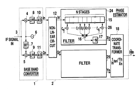
In Fig. 1, there is shown the first embodiment of a
carrier phase estimation apparatus according to the present
invention. As shown in Fig. l, the carrier phase estimation
apparatus comprises a base band converter 1 and a phase
estimator 2. The base band converter 1 has the same
construction and function as that of the conventional
carrier phase estimation apparatus described above and thus
a detailed description thereof can be omitted for brevity.
The phase estimator 2 includes a non-linear circuit 12) a
pair of filters 24 and 25 and a coordinate transformer 18.
In the phase estimator 2, the non-linear circuit 12 and the
coordinate transformer 18 have th~~ same constructions and
-24-
~1I3I3~
functions as those of the conventional carrier phase
estimation apparatus. The filters 24 and 25 input the in-
phase component In' and the quadrature component Qn' of the
digital base band signal) respect=ively, and execute a
filtering. The filter 24 has the same construction as the
filter 25. The filter 24 includes N stages of shift
registers 15, N number of multipl_Lers 26 connected to the
respective shift registers 15 for multiplying the signal
stored in each register 15 by a w<~ighting factor Cx, an
adder 16 and a divider 17.
The operation of the carrier phase estimation apparatus
shown in Fig. 1 will now be described in connection with
Fig. 12 and Fig. 13 which were re=Perred to during the
explanation of the conventional carrier phase estimation
apparatus.
In Fig. l, the base band converter 1 inputs a received
IF signal 3 and outputs an in-phase component In and an
quadrature component Qn of a digital base band signal. As
shown in Fig. 12, the components In and Qn (n = 1 to 5) of
the digital base band signal, fluctuating due to fading, are
input to the non-linear circuit 12 in the phase estimator 2.
The non-linear circuit 12 performs a non-linear conversion
of the components In and Qn and outputs an in-phase
component In' and an quadrature component Qn' of the digital
base band signal, as shown in Fig. 13. The in-phase
component In' of the digital base band signal is output from
the non-linear circuit 12 to the :Filter 24.
-25-
~1I3~35
In the filter 24, the in-phase component In' is input
to the shift registers 15 and the multipliers 26 multiply
the in-phase component In' input into the~respective shift
registers 15 by suitable respective weighting factors Ck at
an input timing of the shift regi~~ters 15. The output
signals of the multipliers 26 are summed by the adder 16 and
the summed value is divided by the filter stage number N in
the divider 17 to output a filter output signal Xn.
In this embodiment, as the feature of the present
invention, as described above, a simple average of the in-
phase component In' stored in the shift registers 15 is not
taken but results of the in-phase component In' multiplied
by the weighting factors Cx, in the multipliers 26, are
averaged.
The filter 25 has the same construction as the filter
24 and operates on the input quads°ature components Qn' of
the digital base band signals in the same manner as the
filter 24 to output a filter output signal Yn.
In the following description, the appendant k of the
weighting factors Ck is determined to 0 in the central stage
of the filter and with separation from the central stage to
the front and rear direction, its absolute value is
determined to be increased, that :is, k = 0, 1, 2, 3, ....)
and an actual value of the weighting factor Cx is determined
to 1 in the central stage (Co = 1) and) differing from the
central stage of the filter, its actual value is determined
to be decreased. Now, for example, it is considered that
-26-
21131 ~~
the weighting factor Ck is represE:nted by formula (9) as
follows .
Ck = 0.7'' .............................. (9)
That is, the signal stored in the central stage of the
shift registers 15 is multiplied by Co = 0.7° = 1, the
signals stored in the two stages adjacent to the central
stage in both the front and rear directions are multiplied
by C1 - 0.71 - 0.7 and further the signals stored in the two
stages which are two stages removed before and after the
central stage are multiplied by C;_ - 0.72 - 0.49.
Fig. 3 shows, in connection with the example shown in
Fig. 13, the values of the components In' and Qn' of the
digital base band signal before the weighting factors are
not multiplied, the weighting factor Ck and the weighted
components Ckln' and CkQn' of the digital base band signal
after the weighting factors are multiplied. As shown in
Fig. 3) the filter output signals X3 and Y3 are calculated
as follows.
X3 - (0.346 + 0.239 - 0.1'l4 + 0.239 + 0.346)/5
- 0.199
Y3 - (0.346 + 0.658 + 0.985 + 0.658 + 0.346)/5
- 0.599
The coordinate transformer 18 receives input the filter
output signals X3 and Y3 and operates according to formula
(4) to output the estimated carrier phase 03, as shown in
Fig. 3.
03 - (1/2)~tan-1(0.599/0.199) - 35.8' ... (10)
-27-
211313a
Essentially, the value of the true carrier phase to be
estimated is 63 - 50° and the est:Lmation error of the
estimated carrier phase obtained in this embodiment is
14.2'. This estimation error is smaller than the 17.1°
which resulted in the conventional carrier phase estimation
apparatus described above. As described above, in this
embodiment, the weighted averaging is used for the
components In' and Qn' of the digital base band signal and
the estimation carrier phase is obtained from the weighted
average value. Hence) according to the present invention,
the carrier phase estimation appa~°atus can well track or
follow up the fluctuation of the carrier phase in comparison
with the conventional carrier phase estimation apparatus.
That is, the carrier phase estimation apparatus according to
the present invention can properly follow up the carrier
phase fluctuating due to the fading.
Fig. 4 illustrates a simulat_Con result of the bit error
rate characteristics realized under conditions shown in
Table 1 by using the carrier phase estimation apparatus in
this embodiment.
Fig. 4 shows the bit error rate characteristics and the
vertical and horizontal axes represent a bit error rate and
a Eb/NO (Eb is the energy per bit and No is the noise
spectral density), respectively. In Fig. 4, white small
circles plot the characteristics of the conventional carrier
phase estimation apparatus and black small circles plot the
characteristics of the first embodiment of the carrier phase
-28-
2113135
estimation apparatus according to the present invention.
Also, a theoretical value shown in Fig. 4 represents bit
error rate characteristics if the estimation error = 0 is
achieved. That is, this theoretical value indicates the
limit of the attainable performan<:e of the carrier phase
estimation apparatus.
TABLE 1 Simulation conditions:
Fading: Ric_Lan Fading
C/P~I~1 - lOdB
fd ~2 - 200 Hz
Modulation: QPSK (differential
encoding)
Symbol rate : 3 . 3'75 kbps
Shift register 9
stage number:
Direct to multipath signal power ratio
Maximum Doppler frequency
As shown, in Fig. 4, in this embodiment, in comparison
with the conventional carrier phase estimation apparatus, it
-29-
2113135
is found that the bit error rate j_s small and a floor value
of the bit error rate (in case of small noise, that is, a
large Eb/NO value, a value of a bit error rate approached to
a fixed value) can be reduced to approximately 1/3. Hence,
it is readily understood that the carrier phase estimation
apparatus according to the presenl: invention can suitably
follow up the fluctuation of the carrier phase due to fading
and realize excellent bit error rate characteristics.
Fig. 4 shows one example of i:he characteristics
obtained by applying the weighting factor Ck represented by
formula (9). However, the weighting factor Cx is not
restricted to this case and, of course, various settings are
possible. For example, the weighi~ing factor Ck can also be
represented by formula (9') as fo7Llows.
Ck = cos(k~/4) (but Ck = 0 when k ? 2) .. (9')
In this case) the weighting factor' Ck is settled such as Co
- 1, C1 - 0.707, Cz, ... - 0.
When formula (9') is applied to the weighting factor
Cx, there is shown in Fig. 15 the result of the bit error
rate characteristics obtained under the same conditions as
shown in Table 1 in a similar manlier to the case shown in
Fig. 4. In this case, from Fig. .L5, it is readily under-
stood that the floor value of the bit error rate can be
further reduced in comparison with the case when formula (9)
is applied. However, in this instance of formula (9'), in
the state that the value of Eb/NO is smaller than
approximately 18 dB, the bit error rate becomes larger than
-30-
2113135
the case of formula (9). Accordingly, a modified system of
the first embodiment described above can be considered.
That is, the state (Eb/NO value) of the channel is detected
and by adaptably or suitably varying the setting of the
weighting factor Ck based on this detected value, better bit
error rate characteristics can be realized. In the above-
described embodiment, when the Eb,'NO value is larger than 18
dB, formula (9') is applied and) vvhen the Eb/NO value is
smaller than 18 dB) formula (9) is applied. In the case
that the Eb/NO value is varied by moving a movable body,
this modified system can realize a smaller bit error rate.
In Fig. 16, there is shown a data demodulation
apparatus to which a modified carrier phase estimation
apparatus for realizing the aforementioned modified system
of the first embodiment is applied. In Fig. 16, compared
with the conventional data demodu=Lation apparatus shown in
Fig. 11, a channel state detector 30 detects the state
(Eb/NO value) of the channel and a factor set circuit 31
sets a suitable weighting factor Cx on the basis of the
Eb/NO value detected by the channel state detector 30 and
delivers the set weighting factor Cx to the phase estimator
2. In this case) the Eb/NO value can be detected by a
statistical processing of demodulated signals. That is) by
carrying out an averaging of the demodulated signals for a
certain degree of real time) a signal power can be
detected and by calculating the variance of the demodulated
signals, a noise signal power can be detected.
-31-
211313
In the modified system of the first embodiment,
although the Eb/NO value is detecl~ed as the state oP the
channel and the weighting factor Ck is set on the basis of
the detected Eb/NO value) for example, it is possible to
detect the fading state such as C,~M (direct to multipath
signal power ratio) or fd (maximum Doppler frequency) and to
determine a proper weighting factor Cx on the basis of the
fading detection. In this case, ~~he channel state detector
30 functions to detect the C/M or the fd.
Next) in Fig. 2, there is shown the second embodiment
of a carrier phase estimation apparatus according to the
present invention. In this embod=invent, as shown in Fig. 2)
a pair of filters 27 and 28 having; the same construction
received as input the in-phase component In' and the
quadrature component Qn' of the digital base band signal
from the non-linear circuit 12 and execute the filtering.
The filter 27 includes the N stages of shift registers 15
and a polynomial approximator 29 which is connected in
parallel with the shift registers 15 and carries out a
polynomial approxima-tion by using the signals stored in the
shift registers 15 to output the :filter output signal Xn to
the coordinate transformer 18.
Next) the operation of the carrier phase estimation
apparatus shown in Fig. 2 will now be described in
connection with Fig. 12 and Fig. :L3 in the same manner as
described above.
As shown in Fig. 12) the components In and Qn (n = 1 to
-32-
211313
5) of the digital base band signa~L, fluctuating due to
fading, are input to the non-linear circuit 12 in the phase
estimator 2. The non-linear circuit 12 performs a non-
linear conversion of the componeni~s In and Qn and outputs an
in-phase component In' and an quadrature component Qn' of
the digital base band signal) as shown in Fig. 13. The in-
phase component In' of the digita7L base band signal is input
from the non-linear circuit 12 to the filter 27 and the
quadrature component Qn' of the same is input to the filter
28.
In the filter 27, the in-phase component In' is input
to the shift registers 15 and the in-phase component In'
stored in the shift registers 15 is input to the polynomial
approximator 29 at the input timing of the shift registers
15. The polynomial approximator 29 approximates the in-
phase component In' by a polynomial expression of n-th
degree and calculates the in-phase component In' at the
timing for estimating the carrier phase by using the
approximation polynomial expression to output a calculated
new value, that is, the filter oui~put signal Xn. In this
case, as described above, n takes values such as n = 0, 1)
2, 3) .... These values represeni~ the relative time
differences between the signals si:ored in the shift
registers 15. That is) in this embodiment, in principle)
the polynomial approximation performs the approximation of
the signals by a time polynomial expression.
The filter 28 having the same construction as the
-33-
2113135
filter 27 operates the input quadrature components Qn' of
the digital base band signals in i~he same manner as the
filter 27 to output the filter oul~put signal Yn.
The polynomial approximator 29 executes the polynomial
approximation by the least square method by using the N
number of signals input to the filter. For instance) it is
considered a quadratic polynomial expression represented by
formula (11) as follows.
PIn' - a + bn + cn2 ... (11)
In this formula, a) b and c represent factors of the
quadratic polynomial equation. By carrying out a quadratic
polynomial equation approximation of formula (11) against
the example shown in Fig. 13, the factors of the approximate
polynomial expression PIn' are obtained such as a = 1.631, b
- -1.068 and c - 0.178. The filter output signal X3 is
calculated by setting the obtained factors a, b and c and by
substituting 3 for n. That is,
X3 - 1.631 - 1.068 x 3 + 0.178 x 32 - 1.129 ... (12)
The same approximation is executed in the filter 28 by using
an approximate quadratic polynomial expression PQn'
represented by formula (13) as follows.
PQn' - a + bn + cn2
The factors of the polynomial expression PQn' are obtained
in the same manner as described above, such as a = 0.512, b
- 0.255 and c = -0.033. As a result, the filter output
signal Y3 is calculated as follows.
Y3 - 0.512 + 0.255 x 3 - 0.033 x 32 - 0.980 ... (14)
-34-
2113135
Figs. 5(a) and 5(b) illustrate the above-described
approximation processing.
The coordinate transformer 18 operates on the filter
output signals X3 and Y3 accordin~; to formula (4) to output
the estimated carrier phase 03. 7Cn this embodiment, the
estimated carrier phase 03 is calculated as follows.
03 - (1/2)~tan-1(0.980/0.029) - 44.2° ... (15)
If it is assumed that no influence of noise or the like
is received, basically, the value of the true carrier phase
to be estimated is 93 - 50' and the estimation error of the
estimated carrier phase obtained In this embodiment is 5.8°.
This estimation error is smaller ithan the 17.1° obtained in
the conventional carrier phase estimation apparatus
described above. As described above, in this embodiment,
the approximation is executed not by simple averaging, but
by the polynomial expression and -the carrier phase
estimation is performed. Hence, it is clear that the
carrier phase estimation apparatus according to the present
invention can properly follow up -the carrier phase
fluctuating due to fading.
Fig. 6 shows the simulation :result of the bit error
rate characteristics realized by using the carrier phase
estimation apparatus in the second embodiment. This
simulation result is obtained under the conditions shown in
Table 1 described above. It is readily understood from
Fig. 6 that, in comparison with the conventional carrier
phase estimation apparatus, when the Eb/NO value is small,
-35-
2113135
nearly equal characteristics can t>e realized and, when the
Eb/NO value is large, the floor of the bit error rate can be
reduced to approximately 1/5. In actual fact, when the
Eb/NO value is extremely small, tree characteristics obtained
in the second embodiment are slightly below the conventional
case. However, there is no problem in practice and it is
readily understood from Fig. 6 that this difference will be
in a negligible range. As described above, according to the
carrier phase estimation apparatus of this embodiment, the
fluctuation of the carrier phase clue to fading can be
properly followed up. As a resull~, in this embodiment) the
bit error rate characteristics can be improved.
As described above, according to the present invention)
the carrier phase estimation appa~°atus having the excellent
follow-up characteristics against the carrier phase
fluctuating due to fading can be obtained. That is)
according to the present invention, the carrier phase
estimation apparatus having excel:Lent bit error rate
characteristics can be obtained.
Although the present invention has been described in
its preferred embodiments with re:Perence to the accompanying
drawings, it it readily understood that the present
invention is not restricted to the preferred embodiments and
that various changes and modifications can be made by those
skilled in the art without departing from the spirit and
scope of the present invention.
-36-