Note: Descriptions are shown in the official language in which they were submitted.
`W093/023~5 21i~3.27J.:.~ PCT/US92/05822
.. . ~
2 MEMBRANE LIGHT MODULATING SYSTEMS
4 Backqround of the Invention
S Spatial light modulators (SLMs) have n~merous
6 potential technical applications such as ~ultispectral
7 infrared target simulation, projection television systems,
8 and optical computer systems. First introduced by Preston
9 in 1968, deformable membrane mirror light modulators
(MLMs), which incorporate a highly reflective membrane as
ll the light modulating element, have generated interest
12 within the applied optics community as good candidates for
13 both adaptive optics and projection display applications.
14 Various means of addressing the two-dimensional deformable
membrane mirror have been demonstrated, including electron
16 beam-addressing, optical addressing, and electrical
17~ addressing via integrated circuits. These devices have
~- ~` ;18~ ~not progressed beyond the development state, hence there
19 are no M$Ms on the commercial market. The electron beam-
addressed approsch is preferred for display applicstions
2l due to the high re~olution and convenience of direct video
22 ~addressing; however, development of suitable substrates
23~ which would decouple the electron beam interaction region
24 from the reflective mirror were lacking. One method of
solving this problem is by introducing the charge-transfer
26 plate (CTP) as a mesns of providing both structural
27 integrity and electrical signal transfer to the mirror
28 elements. This approach has improved the state-of-the-art
29 by yielding a device with a large number of resolution
30 lelements,~ high contrast, and low voltage operation. (see
-31 U.S. patent 4,794,296 assigned to the assignee of this
~2 application)
33 Such a system is shown in Figure 18 of the above
34 referenced '296 patent and is more particularly described
on column 15, lines 21 through 38 thereof. The charge
8UBSTITUTE SHEEl'
WOg3/02375 PCT/US92/05822
~3~ 2-
1 transfer plate creates a two-dimensional electric field
2 which produces a local displacement of the metalized
3 reflective membrane to provide local modulation of the
4 phase output of the two-dimensional light signal reflected
from the mirror. These SLMs exhibit very fast response
6 times, can be read out with high optical efficiency, and
7 in principle can incorporate a very large number of
8 resolution elemen~s. Since a deformable mirror SLM is
9 essentially a two-dimensional phase modulating element
with a large phase dyna~ic range, it is well-suited to
11 adaptive optics applications such as wavefront correction,
12 laser beam steering and phase only spatial filtering.
13 With appropriate pixelization of the membrane surface,
14 intensity modulation may be accomplished via the schlieren
readout schemes employed by projection display systems
16 such as the Eidophor (G.E.) and the Y-Ruticon (Xerox).
17 Recent improvements in the MLM and the system for
18 modulating the charge thereon have involved a M~M wherein
19 a membrane is deposited over an array of wells with an
20 ~addressable electrode at the bottom of each well. Thus,
21 the well and its electrode define an individual pixel.
22 The membra~e is coated with a thin light reflecting
23 electrode material held at a static potential. A pixel is
24 activated by establishing a potential difference between
the well electrode and the membrane electrode, causing the
26 membrane to deform into the well region in response to
27 electrostatic forces. Hence, the pixel driving voltage
28 induces a local phase modulation on the readout wavefront
2g reflected by the membrane mirror surface. Such a system
ds described in "Electron Beam Addressed Membrane Light
31 Modulator", Spatial ~ight Modulators and Applications,
32 1990 Technical Digest Series, Vol. 14, Optical Society of
33 America, Sept. 1990.
34 Brief Summary of the Invention
In one preferred form of the invention a membrane
~,
; ~- 36 light modulator utilizes a charge transfer plate membrane
8UBSTITUTE SHEET
W093/02375 2 ~ ~ 3 2 7 ~ PCT/USg2/05822
--3--
1 anode assembly. The charge transfer plate which has a
2 multiplicity of conductors extending from the rear surface
3 to the front surface of the plate. The conductors are
4 supported in an insulating matrix and the front side of
the transfer plate has a plurality of reces~sed wells
6 defined by insulating walls, each recessed well
7 constituting a pixel. A plurality of conductors are
8 preferably provided for each pixel and a metal electrode
9 in the bottom of each recessed well preferably spans a
plurality of the conductors. The rear surface of the
11 plate preferably includes a secondary electron-enhancing
12 coating. A deformable reflecting metal surface spans the
13 recessed wells. This metal surface can comprise a thin
14 sheet of unsupported metal, but is preferably formed of a
metalized coating on a thin insulating (e.g. plastic)
16 support.
17 In another form of the invention, the anode assembly
18 is such that the support for the mirror membrane is still
19 a plurality of insulating walls defining potential wells
with an electrode on tbe bottom of each potential well.
21 However, the potential wells are not part of a charge
22 transfer plate and the electron beam directly addresses
23 the mirror membrane to modify the charge thereon by either
24 electron depletion or electron accretion.
In addition to electron beam addressing of these anode
26 structures with a cathode ray tube, optical addressing by
27 means of a photocathode and microchannel plate assembly,
28 field emitter array or hard-wire addressing are also
29 possible for each of the anode structures cited herein.
31 Detailed Deacription of the Invention
32 In order to more fully comprehend the invention
33 reference should be had to the following detailed
34 description of several preferred forms of the invention
taken in connection wi~h the attached drawings herein:
36 ~Figure 1 is a schematic view of an overall system
8UBSTITUTE SHEEr
W093/0~75 PCT/US92/0~22
~32~ 5 -4-
1 employing an electron-addressed membrane light modulator
2 (e-MLM) in an image projection system.
3 Figure 2 is a schematic sectional view showing a
4 charge transfer plate, metalized membrane and associated
S electronic and optical components which is an improvement
6 over that prior art CTP illustrated in the'cited 1990
7 technical digest.
8 Figure 3 is a schematic, partial sectional view of one
9 type of charge transfer plate.
Figure 4a is a photomicrograph of a metalized membrane
11 overlying a charge transfer plate.
12 Figure 4b is the light distribution showing the
13 sixfold svmmetry of the Fourier transform of the membrane
14 mirror of 4a.
lS Figure S is a schematic sectional view of a preferred
16 form of the invention.
17 Figure 6 is a block diagram of a comparison between
18 grid stabilized and fr~med video operation of the e-NLM.
19 Figure 7 is a diagram of an optically-addressed form
of the invention, utilizing a photocathode and an electron
21 multiplier assembly a set of microchannel plates to
22 ~roduce the necessary charge image as input to the MLM
23 anode assembly.
24 Figure 8 is a form of the invention, similar to that
of Figure 5, except that the electron beam-addressing side
26 of the CTP is patterned so as to realize an integrated
27 grid in registration with the readout side in order to
28 provide improved charging efficiency of the pixel
. ~
29 electrodes, and reduce crosstalk between pixels.
30 i Figure 9 is a version of Figure 1 modified to
31 accommodate long-wavelength IR projection which re~uires
32 cryogenic cooling of the system.
33 Figure 10 is a form of the invention in which an
34 insulating substrate (face plate) used in lieu of a CTP.
3S~In this form, the electron beam-addressing and the optical
- ~36 readout are achieved on the same face of the device.
-:~ 8UBSTITUTE SHEEr
W O ~3/02375 2 1 i 3 2 7 ~ PC~r/US92/05822
--5--
1 Figure 11 is a form of the invention similar to that
2 of Figure 10, except that rather than a discontinuous
3 metal mirror coating on the membrane, a uniform dielectric
4 mirror is coated onto the membrane.
Figure 12 is a form of the invention s~imilar to Figure
6 11, except the device is addressed and re~d out on
7 opposite sides of the substrate. This is achieved by use
8 of a mirror layer embedded within the insulative well
9 structure.
Figure 13 depicts the electron gun tube enclosure and
11 readout optics which would be used with the device anode
12 architectures of Figures 10,11, or 12 in those cases where
13 the electron beam and optical readout may occur upon the
14 same surface of the well structure.
Figure 14 illustrates a form of the invention which
16 utilizes a field emitter array to produce the necessary
17 charge image oh the charge transfer plate.
8 Pigure 15 illustrates a form of the invention wherein
9 the charge transfer plate pixels are hard wired to an
electronic controller.
21 Figure 16 shows the use of the electron addressed
22 membrane light modulator (e-MLM) to achieve three color
23 projection video.
24 The membrane light modulator of the present invention
can be used in a number of applications. These involve
26 various~`types of high definition display techniques, such
27 as high definition television projection, infrared target
28 simulation, as well as other light modulating systems
29 wherein the spatially modulated light 11 is input to
another device, for example, an optical computer. For
31 simplicity, the invention will be initially described in
32 its preferred form where it is used as an ultraviolet,
33 visible or IR image projector. This initial description
34 is noé intended to limit the scope of the invention in any
way.
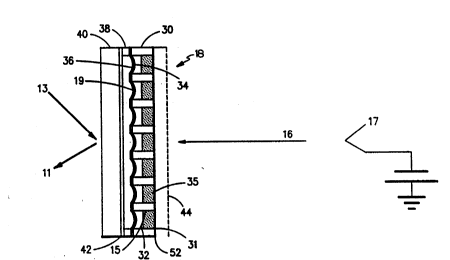
36 A schematic of the projector is shown in Figure 1.
.- ~
8UBSllTUl~ SHEEl-
W093/0237~ PCT/USg2/0582
2 ~ ~32~ 3 -6-
1 Specifically, it consists of a readout light source 10 of
2 the appropriate wavelength which can be a laser, arc lamp
3 or glowbar, for example. It also includes IR collimating
4 optics generally shown at 12, a computer 14 controlling an
electron beam-source 16 addressing a membra~ne light
6 modulator anode 18. Fourier Transform (FT~ spatiàl filter
7 20 and an output device, which may be a high gain screen,
8 detector or video camera 24, are provided for viewing the
9 output image. As will be more fully described, the image
is impressed onto the mirrored membrane surface 34 of the
11 e-MLM by the video signals of the scanning electron beam
12 16, and read out by the reflected light as a phase
13 modulation. The phase modulated beam is then converted to
14 a high-contrast, collimated image by the FT spatial filter
20, and displayed in projection.
16 The construction of a prior art membrane light
17 modulator (MLM) anode 18 which has been improved in
18 accordance with one preferred form of the invention is
19 shown in Figure 2. A membrane is deposited over the front
surface 19 of a charge transfer plate 30 that is patterned
21 with an array of recessed wells 32 defined by insulating
22 walls 15 and having an addressable electrode 35 at the
23 bottom, each such recessed well 32 constituting a pixel.
24 Thus, the well 32 and its electrode 35 define an
25- individual pixel or resolution element as described in the
26 1990 technical digest. Additionally, a secondary electron
27 emitter enhancer coating 31 is deposited on the rear
28 surface 52 of the charge transfer plate 30 that receives
29 the electron signal. The purpose of this coating is to
enhance the depletion of charge from the surface so images
31 of either positive or negative charge can be written
32 efficiently. The membrane 34 is coated with a thin
33 electrode material 36 held at a static potential. This
34 electrode material is hiqhly reflecting and also acts as a
mirror. A pixel is activated by establishing a potential
36 difference between the well electrode 35 and the membrane
8UBSTITUTE SHEET
wo g3/0237s 2 1 ~ 3 2 7 5 PCT/US92/05822
1 electrode 36, causing the membrane 34 to deform into the
2 well region 32 in response to the electrostatic force
3 created by the charge on the pin 35. Hence, the pixel
4 driving voltage induces a local phase modulation on the
S readout wavefront 13 reflected by the membrane mirror
6 surface 36. Since pixel wells 32 are clo~e-packed with
7 high spatial uniformity, the membrane 36 diffracts light
8 efficiently when deformed into the wells 32. By using a
9 schlieren readout scheme 21 (e.g., low pass spatial filter
that passes only the zero-order light or a band pass
11 filter that passes only the first-order light), the phase
12 object at the deformed membrane surface 34 may be
13 converted to an intensity image at the screen 24.
14 The e-MLM consists of an addressing electron beam 16
and an MLM anode assembly generally indicated at 18, as
16 illustrated in Figure 2. The anode consists of a meta~
17 mesh grid 44 before the pixelated matrix of wells 32, over
18 which~the polymeric, metalized membrane 34 is deposited.
19 The membrane 34 is environmentally protected by an
hermetically sealed, IR-transmissive end window 40. For
21 use at infrared wavelengths the window material is
22 preferably zinc selenide (ZnSe) or germanium, whereas
23 materials such as glass could be used in the visible and
24 quartz in the ultraviolet. Both sides of the window 40
are anti-reflection (AR) coated to eliminate undesirable
26 light reflected by the window.
27 Referring still to Figure 2, the electron beam 16
28 writes a charge pattern onto the addressing side of the
29 CTP 30, which is transferred to the bottom of the well 32
30 Iby the electrodes 35 as a two-dimensional voltage
31 pattern. The resulting deformed mirror membrane 34,36
32 phase-modulates the reflected IR readout light 13, which
33 is converted to a projected high-contrast image by the
34 downstream schlieren optics generally shown at 21. (see
3S Figure 1)
36 ~ The heart of the anode assembly 18 is the pixelated
8UBSTlTUTi E SHEET'
W O 93/02375 PC~r/US92/0582~ 2~32~ 5 -8-
1 strueture, called a eharge-transfer plate CTP 30. The
2 name derives from its ability to serve as a high-density
3 multi-feedthrough vaeuum interface, transferring a two-
4 dimensional charge distribution from vaeuum to air. The
CTP 30, illustrated in Figure 3, is a wafer of
6 eleetrieally insulating material 37 in whie~ are imbedded
7 a regular matrix of thousands to millions of
8 longitudinally oriented conduetive pins 35. The ratio of
9 collective pin cross-seetional area to the CTP area is
about 50%. Charge transfer plates 30 with 10 ym diameter
11 pins on 14 ~m eenters, and S0 ym diameter pins on 70 ym
12 centers are typical. Material may be removed from the
13 pins 35 on one side of the plate 30 so as to form a
14 regular array of recessed wells 32 a few microns deep.
lS The surface is highly polished to an optical flatness of 2A
16 across the aetive diameter. Thereafter the enhaneer
17 eoating 31 is applied to the rear surface 52 of the
18 eharge transfer plate 30 by thin film deposition
19 teehnigues.
A polymeric membrane 34 is deposited on the CTP
21 surface that eontains the wells 32 sueh that a reliable
22 bond between the two dieleetric surfaees is established
23 due to van der Waals forees. The resultant membrane
24~ pixels then assume the symmetry of the wells 32 whieh may
be eireular pixels on~hexagonal elosed paeked (HCP)
26 eenters or cireular pixels on square eenters, for example.
27 Upon optieal readout of the membrane 34, this symmetry
28 (square or hexagonal) is preserved in the Fourier plane as
29 a diffraction pattern. A high-magnifieation photograph of
bhe pixelated membrane surfaee with HCP symmetry and its
31 optieal Fourier transform are illustrated in Figures 4(a)
~ and 4(b), respeetively.
33 Referring again to Figure 2, we see that one means of
34 addressing of the MLM anode 18 is aeeomplished by direetly
~;~ 35 addressing the (CTP 30) with a seanning eleetron beam 16.
36 This approaeh offers the following advantages:
~: ~ 8UBSTITUTE SHEET
W093~0237~ 2 1 ~ ~ 2 7 ~i PCT/US92/0~822
_g _
1 (1) With ~he appropriate electron gun drive
2 electronics and high-resolution te.g., vidicon-
3 type) electron gun, each pixel (pin 35) of the
4 CTP anode is individually addressable;
S . ~ :
6 (2) The electron beam current of conv~ntional
7 delivery systems can be large, ranging from tens
8 of nanoamperes to hundreds of microamperes;
(3) A well-established technology standard exists for
11 scanning electron beam imaging systems, as a
12 result of the widescale development of cathode
13 ray tubes and video-based communications (e.g~,
14 television).
Electronically, the e-MLM may be viewed as a triode
16 structure, as illustrated in Figure 2. The thermionic
17 cathode 17 at Vk<0 emits a primary electron beam 16 which
18 may be intensity modulated by its video grid (not shown),
19 which strikes a pin 35 (or pins) of the CTP 30. Secondary
electrons are emitted from the enhancer coating 31
21 overlying the pins 35 and collected by the qrid 44,
22 resulting in a buildup of positive charge on the pin 35 if
23 the secondary electrons are collected by the grid 44. The
24 local potential of the CTP 30 (which influences the
landing energy of the primaries) is determined by the
26 membrane potential at Ym. The landing energy Ep of the
27 primaries is given by:
28 Ep - e(V~ V~.
29 The ratio of secondaries to primaries, or ~, is
dictated by the particular value of Ep. In the absence of
31 an erase cycle, the throughput ~TP) of the e-M$M may be
32 gîven by:
33 TP ~pixels/sec) = is/CV,
34 where iS is the secondary current, C the pixel
capacitance, and V the potential difference required to
36 deflect the membrane 34 to full-contrast modulation.
8UBSTITUTE SHEET
W O 93/02375 rl ~ P(~r/US92/0582~ 2~3~ -lo- : i
1 The throughput is representative of the signal rate of
2 the e-MLM for information proeessing. For example, if we
3 desire a 250x250 pixel image framed at 100 Hz, the TP
4 assoeiated with this frame rate is: TP = 250x250xlO0 =
6.25 x 106 pixels/sec. Henee, the seeondary eleetron
6 eurrent required would, given a pixel eapae'itanee of 0.5
7 pF and a full-modulation voltage of 70V, be:
8 iS=TP C V=(6.25xlO6pixels/see)(SxlO~13F/pixel)(70V)=220 ~A.
9 This level of primary eleetron eurrent is readily
attainable by eonventional CRT-type eleetron guns.
11 In the framed mode, the grid 44 is grounded and a
12 potential differenee is established between the CTP pins
13 35 and the grid 44 by applying a ne~ative DC potential to
14 the membrane metalization layer 36, which drives the CTP
pins 35 to that potential by eapaeitive division. As the
16 eleetron beam 16 seans aeross a eonduetive pin 35 of the
17 CTP 30, seeondary eleetrons are emitted from the enhaneer
18 eoating 31 eovering that pin (35) and are eolleeted by the
19 grounded, planar fine mesh grid 44 held in elose proximity
to the CTP surfaee. Sinee the number of seeondary
21 eleetrons emitted per ineoming primary eleetron, or ~,
22 exeeeds unity, a net positive eharge aceumulates on the
23 pin 35. If an enhaneer eoating 31 is added to the CTP 30,
24 this increases the eharging eurrent is aeeording to the
inerease in ~ of the enhaneer material:
26 -- is2 ~2-
27
28 is~
29 Where ~1 and ~2 are the seeondary eleetron emission
30 !eoeffieients without and with the enhaneer eoating 31. If
31 the eleetron beam 16 eontinues to address that pin 35,
32 eharge accumulates until the pin potential stabilizes to
33 the grid potential, ti.e. ground in this case). During
34 framed operation, the beam eurrent 16 can be eonstrained
sueh that no pixel 32 is allowed to saturate to the grid
36 potential. Thus, by dynamieally varying the electron beam
~3UBSTITUl-E SHEEr
` W O 93/02375 2 1 ~ 3 2 7 ~ PC~r/US92/05822
1 current 16 at each pixel location 32, a continuously
2 varying two-dimensional charge image can be written onto
3 the conductors 35. This results in a voltage drop between
4 the membrane 34 and the pins 35 and the associated
electrostatic force pulls the membrane 34 into the well
6 32. Since the pixel capacitances may be on~~he order of a
7 picofarad, charge storage times can be long (>lOOs). This
8 necessitates an erase cycle following each write cycle;
9 erasure is easily accomplished by grounding the membrane
electrode 36 during electron beam addressing.
11 The device may then be read out by reflecting
12 collimated light 13 off the deformed membrane 34 at a
13 shallow (~10) angle of incidence, as indicated in Figure
14 1. Alternatively, it may be read out at normal incidence
with the use of a beam splitter. The phase information
16 encoded upon the reflected wavefront is then processed by
17 Schileren optics, shown generally at 21 in Figure 1. The
18 schlieren system 21 consists of a converging lens 23,
19 field stop 25 a spatial filter 20 and a reimaging lens 22
as illustrated in Figure 1. The converging lens 23 yields
21 the Fourier transform (FT) of the phase object (i.e., the
22 deformed membrane surface) one focal length after the
23 lens. The FT is a diffraction pattern consisting of
24 bright spots of light that possess the symmetry of the CTP
30, as illustrated in Figure 4(b) for a HCP symmetry. For
26 a fully undeformed membrane surface, only the zeroth, or
27 specular, order is present in the FT plane. As pixels 32
28 are deformed, the diffraction efficiency into the higher
29 orders increases. In the preferred zeroth-order readout
Ischeme an intensity-modulated image of the phase object is
31 obtained by passing only the zeroth order of the FT
32 through the spatial filter 20 before reimaging with the
33 second lens 22. This output image is both collimated and
34 parfocal, and can be displayed onto a screen 24 with
varisble magnification by a subsequent projector lens. As
36 expected, the zeroth-order readout results in a contrast-
SUBSTITIJTE SHEEr
WOg3/02375 PCT/US92/0582~
2~3~ 12-
1 reversed image, i.e., black pixels on a white field.
2 A most important aspect of manufacturing the e-MLM is
3 the fabrication of the pixel structures 32 on the readout
4 side of the MLM anode 18. As indicated in Figure 2, one
- S method of forming pixel structures 32 is by etching away
6 portions of the CTP pins 35, leaving the pe'r~orated
7 insulating substrate 37 as a support structure for the
8 reflective membrane 34. While this prior art method of
9 producing the "mirror" pixels has proved satisfactory it
can be improved. One method has been mentioned above when
11 the secondary emission of the electron impact surface has
12 been increased by use of the enhancer coating 31. Another
13 problem is that the periodicity of the CTP 35 pins may not
14 be perfect. Accordingly, periodicity of the membrane
pixels 32 would not be perfectly periodic. This lack of
16 regularity leads to high spatial frequency, static 'noise'
17 in the reconstructed image. Another related problem is
18 that of image contrast. Since image contrast in a
19 schlieren imaging system 21 is attained by interference at
the image plane, the apparent pixel fill factor is of
21 extreme importance. For example, approximately 50~ pixel
22 fill factor is necessary in order to achieve a perfect
23 intensity null in an anode 18 with HCP pattern of pixels.
24 Another issue is that of dynamic range. ~n order to
modulate long-wavelength-light, membrane deflections of
26 several microns may be required. In order to enhance
27 speed, low ~oltage operation is preferable. To meet these
28 requirements, the ratio of pixel diameter to pixel well
29 depth must be large. For example, it can be shown that
lthe membrane deflection can be expressed by:
31 ~ = (Eo/32) TV2 (a/D)2,
32 where ~ is the membrane deflection, ~O the permittivity of
~ 33 free space, T the membrane surface tension, V the applied
; 34 voltage, a the pixel diameter, and D the pixel well depth.
3~5 Therefore, larger deflections and/or lower operating
36 voltages will be attained by increasing the a/D ratio of
:" ~
- ~ : 8UBSTITUTE SHEET
W093/0~75 2 1 ~ 3 2 7 ~ PCT/US92~0s822
-13-
.
1 the pixel geometry. In addition, the maximum deflection
2 required for deviee operation should be a fraetion (<20%)
3 of the total well depth in order to preserve the parabolic
4 shape of the deflected membrane. This represents about
S half of the defleetion range of the membran,e pixel. Sinee
6 larger defleetions require deeper wells, w~ile low voltage
7 operation implies shallower wells, the optimization of
8 pixel well depth (or a/D ratio) can be determined
9 empirically. This provides the ability to continuously
vary the geometry of the pixel array and achieves the
11 optimization of deviee performanee.
12 As diseussed above, a most important aspeet of
13 manufaeturing the e-MLM is the fabrication of the pixel
14 struetures 32 of the M~ anode 18. Figures 2,5,8,10,11
and 12 show a variety of different anode pixelization
16 sehemes. In the Figure 2,-for example, the prior art
17 eonstruetion pixelization is provided by the CTP 30 on
18 both the addressing side and readout side of the CTP 30.
19 The pixel well struetures 32 are formed by etehing away a
few mierons of the CTP pins 35, leaving the perforated
21 insulating substrate 37 as a support strueture for the
22 membrane 34. Therefore, the strueture of the membrane
23 pixels 32 is tied to that of the CTP 30, in pixel
24 diameter, pixei piteh, periodieity, paeking density, and
25 `so on. ~ As mentioned this form of the invention ineludes
26 the improved enhaneer eoating 31.
27 Several superior arehiteetures ean be employed that
28 deeouple the pixel array from the CTP inter-pin piteh.
29 One sueh improved arehitecture is illustrated, for
!examplej in Figure 5. In one sueh ease, the membrane
31 pixels 32 are ereated ~y patterning an image thereof onto
~2 a thin dieleetrie film S8 eoating the faee of the CTP 30
33 via photolithographie teehniques. In this proeess a
34 dieleetrie film 58 is deposited on the faee of the CTP 30
35 ~with~eonventional spin eoating or vaeuum-deposition
36 teehnioues. The uniformly thiek 2-10 pm eoating is
8UBSTITUTE SHEET'
W093/02375 ~ 14- PCT/USg2/0582
1 overcoated with photoresist which is then exposed by UV `
2 light through a mask. After developing the photoresist,
3 the unwanted dielectric material is removed via plasma
4 etching or wet etching to produce a regular array (e.g.
S rectangular or hexagonal) of say, 100 ym diameter circular
6 pixels on a 138 ~m pitch assuming a 70 pm C~P pin pitch.
7 A layer of metal 56, 1000 angstroms thick is then
8 deposited over the remaining surface. When the
9 photoresist is stripped, the remaining metal pattern 56
defines circular pads at the bottom of each pixel 32 by
11 the metal lift-off technique.
; 12 The dielectric layer 58 has good mechanical properties
13 and provides a smooth surface for membrane attachment.
14 The immediate benefits of this process are twofold: first,
the pixel periodicity and lattice geometry are of the
16 ~ighest quality due to established mask-making techniques
17 and alignment procedures. This~removes fixed-pattern
18 noise from the schlieren optics image plane. Second, the
19 pixel fill factor, pixel pitch, and well depth are
adjustable in a defined fashion, allowing the structure to
21 be optimized for specific optical wavebands and various
22 applications.
~- 23
24 EXAMPLE I
- In one preferred form of the invention of Figure 6,
26 the charge-transfer plate 30 is made according to the
27 methods described in United States Patent No. 4,863,759.
28 The plate is then polished to an optical finish and coated
1 29 with a polymer (for example polyether-imide) to obtain,
i I 30 say, a 3 pm dielectric layer. The polymer is then
31 overcoated with, say, a 2 pm layer of positive
32 photoresist. The photoresist is soft-baked and exposed to
33 a collimated W beam passed through a high-contrast mask.
34 After exposure, the photoresist is developed and the CTP
30 is~placed in a ~lasma chamber. Pixel wells 32 are
36 formed by the removal of polymer material where no
k~
~ ~,
SUBSlTllJTE SHEEl'
W0~3/02375 2 13 ~ 2 7 ~ PCT/US92/05822
--15--
1 photoresist remains. After removal from the plasma-etch
2 chamber, the CTP structure is placed in a vacuum coater
3 where a metal layer 56 is deposited by e-beam or thermal
4 evaporation. Typically 1000 angstroms of aluminum can be
deposited. Upon removal from the vacuum coater, the
6 remaining photoresist is stripped, causing'the metal
7 pattern 56 to remain only in the bottom of the pixel wells
8 32.
9 The metalized membrane 34, preferably Parylene, grown
by plasma polymerization by Lebow Co. for example, is
11 coated with metal 36 prior to attachment to the support
12 substrate. Silver is usually employed as the reflective
13 metal, though other environmentally-robust metals can also
14 be used. The membrane 34 is attached by slowly bringing
it into contact with the substrate under 'tip/tilt'
16 control. The adhesion is due to van der Waals forces
17 which depend on materials parameters of both the substrate
18 and the membrane 34.
19 To optimize the characteristics of the membrane mirror
34, 36 including its zeroth order reflected energy content
21 in the undeflected state, the membrane 34 or underlying
22 substrate may be composed of materials that reduce the
23 tension in the membrane 34 or that reduce the rest-state
24 deflection of the membrane 34 through materials parameters
such~-as Young's modulus of elongation. Alternative
26 membrane materials such as nitrocellulose, polyether-
27 imide, polypropylene, PTFEP, (poly
28 [bis(trifluoroethoxy)-phospazenel), polyimide, polyimide
29 siloxane, or PET (polyethylene terephthlate) may optimize
Ithe actual device performance and are compatible with the
31 process outlined here. Several substrate materials are
32 similarly compatible with this process, including:
33 polyimide, novolac resins, and PTFEP.
34 Alternative processes include direct patterning of
photosensitive polymers ( W -curing adhesives,
36 photosensitive polymide, or photoresist) and similar
8UBSTITUTE SHEEl~
W093/0~7~ PCT/US92/05822
~3~ 16~
1 patterning of vacuum-deposited (evaporated or sputtered)
2 dielectric films (such as ZnS, MgF2, SiOx, Y2O3, or
3 cryolite).
4 In summary, this improved approach for pixel
construction on the MLM anodes has the following
6 advantages: ~
8 Improved contrast due to reduced rest-state
9 membrane pull-back
11 Enhanced pixel-to-pixel uniformity of response by
12 improving the uniformity of the pixel geometry.
13 Reduced or eliminated fixed-pattern noise from
14 the image by achieving a high degree of
periodicity in the pixel array.
16
I7 Improved image contrast to at least 200:1 by
18 'tuning' the pixel fill factor.
19
Phase dynamic range tailored to the specific
21 waveband of interest by controlling the ratio of
22 pixel diameter to pixel well depth.
23 Due to the effi~ient charge storage characteristics of
24 the CTP 30, considerable image storage times (>103 sec)
have been observed in the e-MLM. Thus, conventional video
26 operation would imply a frame erase after each video
27 fieldO Since this is wasteful of charge, and also results
28 in non-negligible image flicker, the flickerless mode of
29 operation is preferred. While the conventional video
30' addressing approach described above applies the video
31 signal to the electron gun control grid in order to
32 modulate the delivered beam current, it is also possible
33 to apply the video signal directly to the membrane
34 instead. Thus, the electron beam current will be fixed
and simply scanned across the MLM anode 18 at video rates.
36 The potential difference across each pixel well 32 will
SUBSTITUTE SHEEl-
W093/02375 2 1 ~ 3 2 7 S PCT/US92/05822
-17-
1 thus be determined by the instantaneous potential applied
2 to the membrane 34 when the electron beam 16 is impinging
3 on that pixel 32, since the pixel pin electrode 35
4 stabilizes to the grid potential by the secondary emission
process. Such a process is referred to as grid-stabilized
6 operation. A similar scheme has been suc~essfully
7 employed in the operation of the Sodern light valve to
8 eliminate flicker from the display. The differences
9 between framed operation and grid-stabilized operation are
illustrated in Figure 6.
11 Apart from the absence of image flicker, the grid-
12 stabilized mode of operation is more charge-efficient than
13 standard video operation by up to a factor of two.
14 In addition to the field of IR target simulation and
scene generation, further developments of this class of
16 dev~ce present distinct advantages to many areas and
17 systems of significant interest to the military.
18 Important application areas of the device include: high-
19 definition flîght simulator displays, infrared scene
projection, laser beamsteering and wavefront correction in
21 optical communications and imaging through turbulence,
22 high-intensity large-format displays for C3I and
23 teleconferencing, robotic vision, autonomous vehicle
24 guidance, pattern recognition, parallel processing of
large knowledge bases, multispectral image fusion, neural-
26 network-based processing, and industrial inspection. It
27 is the unavailability of low-cost, high resolution, high
28 brightness SLMs that is impeding the development of all
29 areas of optical signal processing and other specialized
30 ! optical systems such as joint correlators and industrial
31 inspection systems. Concerning the multi-billion-dollar
32 display market, this technology can benefit the high-
33 definition large-format projection displays for television
34 conference rooms, auditoriums and the home.
35~ While one embodiment of the invention has been
36 ~described above wherein an electron beam 16 is scanned
8UBSllTUTE SHEEr
WOg3/0~75 PCT/US92/05822
~ 3~ 18- ~ ~
1 across the rear of the transfer plate 30 to create an
2 image modified spatial charge on the light modulating
3 membrane 34, other methods of creating the space charge
4 image can be uti}ized as shown in Figure 7. In this case,
S the write signal 63 is an image incident on a photo-
6 electron emitting layer 60 carried on an i~p~ window 61.
7 This photo-electron emitting layer 60 emits an image
8 modified stream of electrons through an electron
9 multiplier assembly shown here as a set of microchannel
plates (MCP) 62 which transfers the amplified stream of
11 electrons to the rear of the charge transfer plate 30
12 operating under the influence of grid 44. This anode
13 structure is preferably made in accordance with the
14 present invention. The charge is transmitted to the front
thereof; the resultant electrostatic forces deform a
16 membrane 34, 36 whose image-modified deflection is read
17 through an output window 40 by suitable readout beam 13.
18 This general arrangement of elements is similar to Figure
19 18 of the above mentioned patent 4,794,296 owned by the
assignee of this application.
21 Another embodiment of the present invention provides a
22 modified grid arrangement on the rear of the charge
23 transfer plate 30. As shown in Figure 8 an electron beam
24 16 strikes secondary emitting portions 70 on the rear of
the charge transfer plate 30. The impacting electrons
26 cause a large emission of secondary electrons which are
27 then collected by a modified grid 44a which is formed on
28 insulated pedestals 72 created by masking techniques
29 similar to the photolithographic masking techniques
discussedjabove for forming the front surface insulating
31 spacer walls 58 in Figure 5.
32 Referring now to Figure ~, in those situations where
33 the light to be modulated has a very long wave length
34 (e.g. 8-14 pm) it is necessary to provide a liquid
'
8UBSTITUTE SHEEr
W093/02~75 PCT/US92/05822
1 nitrogen cooled jacket 50 to surround the whole system so
2 as to suppress background infrared radiation that could
3 interfere with and mask the IR image being processed by
4 the system. Jacket 50 in turn is surrounded by a thermal
shield 71 has a port 85 for charging the jacket with
6 liquid nitrogen and a port 79 for interconn-ecting the
7 enclosure 86 to a vacuum system (not shown). A collimated
8 beam from an IR light source 81 is directed through a set
9 of baffles 78 onto the Infrared Membrane Light Modulator
(IRMLM? 76. The modulated IR light is reflected onto a
11 combination of two Fourier Transform Mirrors 83 and a
12 magnetically controlled spatial-filter mirror 75 as
13 follows: the modulated IR light is first reflected to one
14 Fourier Transform Mirror 83, then onto the spatial-filter
mirror, then back to a second Fourier Transform Mirror
16 from which it is directed at the system under test 74.
17 The IRMLM is directed by a controller 77.
18 In the above discussion of the preferred form of the
19 invention, the electron stream or beam 16 addresses the
rear surface 52 of the charge transfer plate 30, and the
21 front of the charge transfer plate 30 carries the
22 metalized membrane mirror 34 which is selectively
23 deflected by the charge transferred through the plate.
24 In a further modification of the invention the
electron beam 16 impinges directly on the metalized
26 membrane 34 of an anode structure 18 that does not
27 necessarily employ a charge transfer plate. In this case,
28 each portion of the mirror constituting an isolated pixel
29 32 is insulated from each other pixel so that an isolated
30 Icharge can be created at each pixel. This modification is
31 shown in Figure 10. where the electron beam 16 strikes the
32 metalized isolated mirror 36 overlying the pixel potential
33 wells 32~ The isolation of the mirror 36 is achieved by
34 gaps 36a in the coating 36. Secondary emission of
electrons will create a static charge on the insulated
~6 mirror 36 in accordance with the intensity and energy of
SUBSTll UllE SHEEl-
~093/02375 PCT/USg2/05822
~3~5 -20- .
1 the electron beam 16. This static charge will then create
2 deformation of the membrane 34 in direct accordance with
3 the charge carried thereby in the same fashion as the
4 deformation of the membrane 34 as discussed in connection
with Figures 2 and 5. In this case, the struçture could
6 be essentially the same as described for F~gure S with the
7 exception that the metalized mirror 36 would have gaps 36a
8 electrically isolating each portion of the metalized
9 mirror 36 overlying the individual pixels 32.
~n Figure 10, the readout light 13 is directly
11 impinged on the mirror surface 36 through the envelope
12 surrounding the source of the electron beams 16.
13 In Figure 11, a similar embodiment of the invention is
14 shown wherein, instead of having individual metal mirror
coatings 36, the reflective surface is created by a
}6 dielectric mirror 90 such as a multiple alternating layer
17 stack of SiO~/TiO2. In this case, electron beam 16
18 impingement charges the dielectric mirror 90 negatively or
19 positively and concentrates the charge at the point of
impact of the electron beam 16. Accordingly, the pixels
21 32 will accumulate an amount of charge depending on the
22 beam current, the dwell time of the electron beam 16, and
23 the secondary electron emission coefficient in the case of
24 positive charging. Thus the membrane 34 will be deflected
into the potential wells 32 in accordance with the charge
26 carried thereon.
27 A similar system is shown in Figure 12 but in this
28 case the readout light 13 is beamed through the support
29 window 40 to the mirror 84. Note that a charge transfer
plate 30 cannot be used as the membrane support since the
31 membrane substrate must be transparent. In Figure 12, a
~2 stack of two transparent insulators 80 defining the
33 potential wells 32 i5 mounted on a transparent electrode
34 82, such as an indium tin oxide layer, and mirror surfaces
84 are provided between these insulators 80. The isolated
8UBSTmJTE SHEET
WOg3/0~75 PCT/US92/05822
-21- 21i327~
.
1 mirror pixels 36 are then supported on top of the second
2 insulator stack 80 provided above the mirror surfaces 84.
3 In this case, readout light 13 is modulated in accordance
4 with the degree of deformation of the individual mirror
pixels 36 into the potential wells 32. The~ contrast ratio
6 of the modulation is dependent upon the re'lative position
7 of the membrane mirror pixels 36 referenced to the mirror
8 surfaces 84 within the insulators 80.
9 In Figure 13 there is shown a schematic assembly of a
readout optical system and a modified electron beam
11 addressed membrane spatial light modulator which directs
12 an image modified electron beam directly on the mirror
13 membrane anodes 36 as illustrated in Figure 10, or 11.
14 While several modifications of the invention have been
described above where an electron beam cathode ray tube
16 scans the charge transfer plate 30 or the mirrored
17 membrane 36 directly, it is also possible to utilize a
18~;source of electrons from a field emitter array 64 which
l9~can be elect:onically addressed. Such a field emitter
array 64 is shown in the copending application Serial No.
21 07/638,317 filed January 4, 1991 and owned by the assignee
22 of the present invention. Similarly, the charge transfer
23 plate 30 can be directly wired by a suitable electronic
24 controller 65 having addressing wires 66 which directly
couple to the rear surface 52 of the charge transfer plate
26 30. Examples of these two systems are shown in Figures 14
27 and 15.
28 Figure 14 shows a field emitting source 64 of
29 electrons which impact any of the anode structures of
Figureæ 2,i 5, 8 or 12 of the present invention.
31 ~ In the direct wired configuration shown in Figure 15
32 an electronic controller 65 drives each of the pixels 32
33 by means of discrete metal electrodes 54 provided on the
34 rear side 52 of the charge transfer plate 30. The other
(mirror) side of the charge transfer plate 30 is made in
36 accordance with the present invention.
SUBSTITUTE SHEEl~
W093/02375 PCT/US92/05822
~ 3~ 22-
1 In Figure 15 the charge transfer plate anode 56 is
2 preferably made as shown in Figure 5.
3 From the above description, it should be apparent that
4 the novel charge transfer plate 30 of the present
invention can be used in a wide range of applications
6 wherever spatial light modulation is desir~d. The input
7 to the membrane anode structure charge transfer plate may
8 be derived from a vast number of different types of
9 electron sources and scanning can be achieved in numerous
ways as described above.
11 An improved high-definition electron-beam-addressed
12 Membrane Projection Display (MPD) System is illustrated in
13 Figure 16 as a three color projection television system.
14 It is comprised of three subsystems as shown: (a) three
electron-beam-addressed Membrane Light Modulators (e-MLMs)
16 41 with their common readout light source 10 and dichroic
17 beam splitters 55, (b) a spatial filtering 20 and
18 projection optical system 43 and (c) an electronic control
19 and computer interface subsystem 45 which performs the
necessary image format conversionæ and implements the
21 control functions that allow the microprocessor to control
22 the light valve.
23 In operation, white light from an arc lamp is fed into
24 the optical system consisting of the three dichroic
beamsplitters (BSl, BS2, and BS3) that extract the blue
26 47, green 48, and red 49 light components, respectively,
27 for readout of the three e-MLMs 41 as shown in Figure 16.
28 Thus e-MLMl 46, for example, which is driven by the blue
29 component 47 of the electronic video signal, phase
modulates only the blue component 47 of the image as it
31 reflects from the deformable membrane mirror surface 36 e-
3~ MLMl 46. Similarly, the modulators e-MLM2 51 and e-MLM3
33 53 modulate the green 48 and red 49 components of the
34 readout beam 13. The modulated zero-order components of
the blue, green and red light are recombined by the second
36 set of dichroic beamsplitters 55 (see Figure 16) to yield
: 8UBSTITUTE SHEEl-
W O 93/023?5 PC~r/US92/05822
23- 2 1 ~ 3 2 7 ~
the~p~a;se ~odulated three color signal beam 57.
2 While numerous modifications of the invention have
3 been described, many additional forms thereof will be
4 apparent to one skilled in the art and the invention is
not to be limited to the specific forms shown~
-
~::
`:
8UBSTITUTE SHEEl- ` ~
, ~