Note: Descriptions are shown in the official language in which they were submitted.
:: 2 t 1 3 4 ~ ~
APPARATUS AND METHOD FOR IDENTIFYING
METALLIC TOKE~S AND COINS
BACKGROUND OF THE INVENTION
1. Field of the Invention
The present invention relates to the sensing and
identification of metal tokens or coins electronically.
More particularly, it relates to method and apparatus
for identifying a variety of currency coins of several
countries with high reliability and without the need of
reprogramming or readjustment. More particularly still,
the apparatus is suitable for yielding unique digital
codes each corresponding to a single coin or token
sensed and identified by the present method. -~
' ~
2. Prior Art of the Invention
It is known to utilize size, shape and electrical
properties of a coin for coin discrimination. For
example, these characteristics affect the coupling
between an excited coil and a detection coil in United
States patent 3,373,856 granted March 19, 1968 to
Kusters et al. The induced voltage in the detection
~t.t ~:
2~3~
coil is rectified and the coin is accepted only if the
rectified voltage lies between two preset levels.
In United States patent 4,432,447 granted February 21,
1984 to Tanaka, essentially the same principle as above
is utilised to sort coins. But, in addition, there is
another coil (3) through which the coin passes, which
coil forms the arm of an excited bridge circuit. The
variable arm of the bridge is adjusted such that it is
normally unbalanced, and is balanced only when the
"true" coin is passing through the coil. The zero
output of the bridge when balanced momentarily is the
indication of the true coin. The circuit is thus
tailored to discriminate between a true coin of a
desired denomination and a particular coin similar in
configuration to the desired coin.
United States patent 4,460,080 granted July 17, 1984 to
Howard, discloses coin validation apparatus utilising a
coil formed in two halves, connected in series with one
half on one side of the coin runway and the other half
on the other side of the coin runway. Capacitors are
connected to the coil to form a resonant tank circuit,
and the effect of a coin on the inductance and loss
factor of the coil is compared to reference values to
determine coin validity.
2 ?/L ~ r~
United States patent 4,742,903 granted May lO, 1988 to
Trummer, discloses several oscillator tank circuits
having different natural frequencies ranging from 120
kHz to 247 kHz. The attenuators of the oscillator tank
circuits are balanced by resistors, so that the high-
frequency voltage which the oscillator exhibits with
each of the tank circuits have the same amplitude in the
absence of a coin. The effect of the coin alloy on the
low frequency test signal is greater, while the effect
of the depth of embossing is smaller.
United States patent 4,895,238 granted January 23, l990,
to Speas discloses a coin discriminator system for use
in an electronic parking meter. A deposited coin is
inserted in the electronic parking meter and a chute
guides the deposited coin past an inductor. The
deposited coin causes a momentary change in the value of
inductance of the inductor. A phase lock loop
electronic circuit has an input connected to the
inductor and the phase lock loop electronic circuit.
The correction signal compensates for the change in -
value of inductance of the inductor and has a wave shape
unique to the deposited coin. A microprocessor receives
the correction signal wave form for comparison to a
plurality of predetermined wave shapes of a plurality of
~r~
~i3~
known coins to thereby identify the deposited coin. The
plurality of predetermined wave shapes are stored in a
memory connected to the microprocessor.
SUMMARY OF THE INVENTION
The present invention utilizes the sensitivity of an ac-
bridge circuit, but one which is normally balanced and
is unbalanced by the passage of a coin or token. The
frequency at which the maximum bridge output occurs, and
the value of that maximum, have been found to uniquely
identify in excess of twenty different coins from
several countries. On the other hand, at a given
frequency, the bridge, when unbalanced, provides a
complex output voltage (including both amplitude and
phase angle) which is a function of the conductivity and
permeability as well as the size of the coin causing the
unbalance.
Indeed, in its broadest aspect, the apparatus and method
of the present invention are capable of identifying and
discriminating several coins or tokens by sensing a
single bridge parameter. For example, phase difference,
frequency or output. However, it is preferred that at
least two such parameters be used to identify tokens.
For example, frequency and output level; phase
'-'" 2~13~n,~
difference and output level; or phase difference and
frequency.
According to the preferred method aspect of the present
invention, an input signal is applied to an ac-bridge, a
coin or token is brought in the vicinity of one arm of
the ac-bridge, an output signal of the ac-bridge is
sensed, and the output signal is associated with
presence of the coin or token in the vicinity of the arm
of the bridge.
According to the preferred apparatus aspect of the
present invention there is provided, a bridge for
coin/token identification, comprising: two inductors of
equal value and two impedances of equal value, one in
each arm of the bridge; signal generating means for
applying a predetermined frequency across an input of
the bridge; and phase detection means at an output of
the bridge.
In a narrower aspect, the phase detection means detects -
a predetermined phase shift between input and output of
the bridge. ;~
In a narrower aspect yet, the phase detection means
controls the frequency of the signal generating means ~-
6 21~ 3,~
until the predetermined phase shift is detected, thereby
detecting a maximum in bridge unbalance.
At maximum bridge unbalance, the predetermined phase
shift is either 180 degrees or zero degrees.
In a further, narrower, aspect, an amplitude detection
means is provided at the output of the bridge.
In yet another, narrower, aspect, the signal generating
means applies a sequence of predetermined frequencies
across the input of the bridge.
In the preferred aspect, the sequence of predetermined i
frequencies is a signal having continuously variable
frequency between predetermined lower and upper
frequencies.
In a more preferred aspect, the continuously variable
frequency signal is repeated until a predetermined
output is detected across the output of the bridge.
~ _ " ~
2~3~ ~
BRIEF DESCRIPTION OF THE DRAWINGS
The preferred embodiment of the present invention will
now be described in detail in conjunction with the
annexed drawings, in which:
Figure 1 is a block schematic of the apparatus for
identifying metallic tokens and coins of the present
invention;
Figure 2 is a more detailed block schematic of the
apparatus shown in Figure l;
.
Figure 3 is a block schematic showing in more detail the
apparatus shown in Figure 2; ~:
Figure 4 is a circuit schematic of the bridge and bridge
amplifier shown in Figure 3;
; Figure 5 is a circuit schematic of the SINE-DAC shown in
Figure 3:
:
Figure 6 is a block schematic of the VCO and phase
detector shown in Figure 3;
Figure 7 is a circuit schematic of a buffer/gating
~S, , ,. ", ,, ~ ~,, ". "~ ~ .",~ ", ~, , , , ~ " ,, ,, ,~
~` 2~3~ 3
circuit between the bridge amplifier and the phase
detector in Figure 3; and
Figure 8 is a pictorial showing two side-elevations of
the bridge coils Ll and L2 shown in Figure 4.
- 2~ 13~ ,~
DETAILED DESCRIPTION OF THE PREFERRED EMBODIMENT
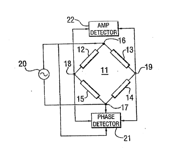
Referring to Figure 1, a general schematic of the
apparatus of the present invention is shown. It
comprises a normally balanced brid~e 11 constituted by
four impedances 12, 13, 14 and 15, and therefore, having
two sets of diagonal nodes 16/17 and 18/19. A signal
generator 20 is applied to the bridge 11 across the
nodes 16/17, while a phase detector 21 is applied across
the nodes 18/19. Also shown is an amplitude detector 22
across the nodes 18/19. For ease of phase detection,
the phase detector 21 is shown having the signal from
the generator 20 as input. In operation, the phase
detector 21 compares the phase of the output signal at
the nodes 18/19 to that at the (input) nodes 16/17 and
indicates the phase difference detected, once the
amplitude of the output signal at the nodes 18/19 is
sufficient to enable such phase comparison; that is, ::
once the bridge 11 is sufficiently unbalanced by the
passage of a coin or token in the vicinity of one of the
bridge 11 arms 12, 13, 14 or 15. It is, therefore,
necessary that at least one of the bridge 11 impedances
be of such nature as to change its impedance value as
the coin or token is brought near it. The amplitude
detector 22 detects the amplitude of the output signal
at the nodes 18/19. Thus, both phase difference and .
? ~
~ ~ , " ,~ ,, , " , " , , , ~ : .
,~ 2,L~ ni~
lo
amplitude are associated, and may both be used as two
parameters unique to each member of a predetermined set
of tokens. On the other hand, one may choose to
associate the value of one of the two parameters, at a
fixed value of the other parameter, the token
identifying parameter. Moreover, the frequency of the
signal applied by the generator 20 may be used as a
third parameter for finer discrimination between tokens,
Thus, if the amplitude is measured always at the point
where the phase difference is 180 (this is the point of
maximum bridge unbalance and, hence, maximum amplitude
at the nodes 18/19), and is found to be the same for any
two coins, then the two frequencies at which this occurs
are used to distinguish one coin from the other.
Accordingly, it is necessary that coins of different
currency or denomination not be identical in all
physical and compositional respects for the present
invention to distinguish them.
Figure 2 of the drawings shows a block schematic,
wherein a microprocessor 23 is utilised to perform
central and monitoring functions of the generator/V~O 20
(voltage cnntrolled oscillator), the phase detector 21,
and the amplitude detector/rectifier 22. Thus, the
processor 23 outputs a staircase signal which is
converted in D/A converter 24 (digital-to-analog) to an
1 1 2 ~
analog voltage to cause the VCO to sweep its frequency
range (approximately lOO to 250 kHz) and accordingly
drive the bridge 11. The output of the bridge 11 is
applied to a bridge amplifier 25 (in order not to load
the bridge and upset its balance/unbalance conditions),
the output of which is applied to the phase detector 21
and the rectifier 22, the output of which in turn is
applied to an AID converter 26 in order that the
microprocessor 23 may associate the amplitudes and
phases detected with the driving frequency, and thus
identify the token causing the bridge 11 unbalance by
comparing the parameter (or parameters) detected with ~.
that stored in its memory. An example of such a table
of parameters stored in the memory for the amplitude and
frequency at the point of 1800 phase difference (between
output and input of the bridge 11) is as follows:
COIN AMPLITUDE FREQUENCY
(Country and (Relative Value in (in KHz)
Denomination) Hexadecimal Notation)
UK - 2p , 88 136.2 :
CAN - lc 96 143.6
US - 25c B6 143.6
US - lOc ('86) DC 150.9
CHILE - 1 peso A7 164.8
UK - 50p AB 168.0
3 ~ ~ ~
12
COIN AMPLITUDE FREQUENCY
(Country and (Relative Value in (in KHz)
Denomination~ Hexadecimal Notation)
YUG - 1 dinar 9D 171.3
FRANCE - 20ct. BA 171.4
FINLAND - lmk A9 178.2
SPAIN - 5 ptas AA 178.2
UK - 5np B0 181.2
US - 5c ('89) B2 181.2
US - 5c ('62) B4 181.2
GER - 1 DM B0 184.4
GER - 50 pf CE 184.4
CAN - $1 56 199.6
CAN - 5c ('65) 8F 208.7
CAN - 25c 80 211.6
CAN - 10c AA 228.6
Figure 3 is a yet more detailed block schematic diagram
of the apparatus. In it, the D/A converter 24 is
replaced by Ramp-and-Hold Circuit 27 controlled by the
microprocessor 23 to increase or decrease its output
voltage in steps ~ramps), thereby incrementally ~or
decrementally) controlling the VCO 20. The latter
sweeps the frequency range up or down. The VCO 20 is
followed by a digital-to-analog convertor SINE-DAC 28,
the output of which drives the bridge 11 at the nodes
13 2 1 1 3 ~
16/17. The output nodes 18/19 of the bridge 11 are
connected to the bridge amplifier 25, the output of
which is buffered before application to the phase
detector 21. A phase difference between the signal at
the nodes 18/19 and that at the nodes 16/17 of 180 (or
0) is signalled to the processor 23 and causes the
Ramp-and-Hold Circuit 27 to hold its instantaneous
voltage ramp, causing the VC0 20 to hold that particular
frequency which corresponds to the 180 phase shift and
also corresponds to the maximum unbalance of the bridge
11 and the maximum amplitude at the nodes 18/19. The
maximum amplitude is rectified by the detector 22 and
digitalized in the A/D convertor 26. The value of the
amplitude is associated with the held frequency of the
VC0 20 by the processor 23 and such combination is used
by the processor 23 to locate it in the memory, thus
identifying the coin as per the table shown above. Of ;~
course, failure to identify the particular combination
of amplitude and frequency results in the coin being ~
rejected as unacceptable. The microprocessor 23 is ~;
alerted to enable the A/D convertor 26 by a "coin in"
signal once the signal from the rectifier 22 exceeds the
threshold set at threshold detector 29.
Figure 4 shows the bridge 11 circuit and bridge
amplifier 25 components. The bridge 11 comprises two
,. . .
2 ~
14
wire coils (inductors) Ll and L2, at the junction of
which (INPUT) the input signal (generated by the VCO 20
and conditioned by the SINE-DAC 28) is applied. The
remaining two bridge arms and resistors Rl and R2 and
the respective sides of fine balancing potention meter
R3, which is used to compensate for slight inherent
unbalances in each individual bridge, and the wiper of
which is connected to signal ground. Thus the input
signal is applied to the bridge 11 input between the
INPUT and ground, that is to a pair of diagonal nodes of
the bridge 11. The output of the bridge 11, connected
to the bridge amplifier 25, is the other pair of
diagonal nodes 30-31.
Figure 5 shows the SINE-DAC 28, which receives its input
from the VCO 20 at clock input of counter 32. The
counter 32 is clocked by the VCO 20 at a multiple of the
output frequency (eight times in the preferred
embodiment) of the buffered signal at VCO OUT, which
drives the INPUT of the bridge 11 and also the phase
detector 21. The VCO OUT signal, since it drives a
relatively low impedance bridge, has low source
impedance provided by complementary transistor pair 33.
The digital-to-analog convertor comprising the counter ~:~
32 and following weighting resistors is of conventional
well-known design.
2 ~
Figure 6 and 7 show the ancillary circuits of the VCO 20
and the phase detector 21, which are actually a single
IC (74HC4046 by Motorola), The signal from the OUTPUT
in Figure 4 is applied via the buffering and gating
circuit of Figure 7 to signal input SIG of the phase
detector 21, to the reference input REF of which is
applied (also via an identical circuit as that of Figure
7) the VCO OUT signal of the SINE-DAC 28. That is, the
phase detector 21 compares the phase of the signal at
the output (30-31) of the bridge 11 to the phase at its
INPUT. It is, of course, clear why all intervening
buffering and gating circuitry such as that in Figure 7
must be identical in order to affect the relative phases
at SIG and REF identically.
Figure 8 shows the physical construction of the wire
coils Ll and L2 of the bridge 11. The coils Ll and L2
are identical windings, but more importantly they must
have the same inductance at the frequency range of
interest, that is from approximately lO KHz to 300 KHz.
Thus the inductance for each coil is 310 microhenrys
plus or minus 1% measured at 250 KHz. The copper wire
is #30 AWG wound in two layers having a total of
approximately 160 turns per coil. The coils Ll and L2
are wound on a rectangular shaped bobbin 34
~'' ' '
~ 2 ~ ~ 3 ~ 9 3~
16
approximately 3 cm in width and 9 cm in length. Each of
the windings Ll and L2 in Figure 8 is 3 cm long and
there is a small separation 35 of approximately 8 mm
between the two windings. The bobbin 34 also serves as
a "chute" for the coins or tokens to be descriminated
and is, therefore, hollow inside having a chute of
approximately ~ mm in width. A coin or token is
deposited through aperture 36 and falls through the
bobbin 34 to exit from its bottom aperture 37. The
bobbin 34 is made from any suitable insulating material
such as a plastic. While in Figure 8 the coils Ll and
L2 are shown arranged in tandem, so that the coin or
token passes through both coils on its way to a
collection box, this is by no means mandatory. For
example, it is quite feasible to position one of the
coils such that a token does not pass through it.
Indeed it may be sufficient that a token merely passes
in the vicinity of one of the coils such that its
magnetic and/or electrical characteristics are
sufficiently altered. Accordingly, it is not a
requirement that the coil (Ll or L2) be wound in the
manner shown in the figure. Depending on the frequency
of the ac-signal applied to the bridge 11, the sensing
coil (or coils) could be, in principle, a single loop of
wire, the plane of which a token grazes. Moreover, if
the tokens to be sensed were all non-magnetic, the coil
y~
- ` 2 ~ 5~ t;1~
17
or loop could be wound on a magnetic core or bobbin. As
may be seen from the following description of the
operation, it is advantageous to arrange the two coils
Ll and L2 in spatial sequence such that a token first
passes through Ll and then through L2, and that they be
identical. But, in general, in a design where a token
passes only through one coil, the second need only be
identical in its electromagnetic characteristics, and
cculd be a component having the same impedance.
Operation:
Two parameters are determined for each coin:
a) the frequency at which the signal driving the
input node of the bridge and the signal at the
output node of the bridge are either exactly in-
phase ~zero degrees) or 180 degrees out-of-phase,
and
b) the amplitude (which is a maximum) of the
signal out of the bridge at the above frequency.
a) The Phase/Frequency Measurement
The input signal generated is a constant amplitude sine-
~., ~ ,
~, ' ' ~ ~ , : '
~"' 2 1 i
18
wave signal covering the frequency range from about 200
kilohertz down to 17 kilohertz. The circuit comprises a
"ramp and hold", a voltage controlled oscillator (VCO),
and a sine-wave digital-to-analog convertor (SlNE-DAC).
The total frequency span is divided into two ranges,
referred to as HI (high frequency range) and LO (low
frequency range) in Figure 3. The high range is
approximately 200 kHz down to 80 kHz and the low range
is approximately 60 kHz down to 15 kHz.
Referring to Figure 3, when doing a measurement, the
oscillator frequency always starts at the highest
frequency for that range and sweeps down to the lower
limit. A typical sweep would be accomplished by first ~-
selecting the HI frequency range and selecting DOWN to
sweep the oscillator frequency from the highest to
lowest frequency. If the required phase relationship is
not detected somewhere in the range, the ramp and hold
are quickly ramped back UP to the maximum voltage, the
range changed from HI to LO, and the oscillator swept
DOWN once again.
A one millisecond active low pulse on the UP line will -
reset the ramp and hold output, VCO and SINE-DAC to the
maximum output frequency for the selected range. A ten~
millisecond active high pulse on the DOWN line will
.
2 ~ 3 ~
19
sweep the drive frequency over the entire range
selected, if detection of the required phase does not
occur. The two control lines for the ramp and hold are
independent of each other and only one should be
asserted at a time.
As a coin enters the first coil of the chute, the bridge
becomes unbalanced and an output signal is generated.
This signal is amplified and converted to a logic level,
as is the reference signal driving the bridge. These
two logic signals are then passed to a phase angle
detector capable of determining when the two inputs are
either exactly in-phase or 180 degrees out-of-phase.
The selection of in-phase or 180 degrees out-of-phase
occurs automatically when the frequency range is
selected. For the HI range, the circuit is checking for
180 degrees phase difference. For the LO range, it is
checking for zero degrees phase difference.
If the appropriate phase relationship is detected, the
phase detector immediately stops the ramp and hold
output, which keeps the oscillator at a fixed frequency
for the remainder of the measurement cycle. This action
overrides the DOWN line. The intention is to very
quickly "freeze" the oscillator at the correct
frequency. This will prevent overshooting of the
,. ' ''' -' ~ :
211~
frequency while the controller (microprocessor 23) is
polling the "PHASE DETECT" signal line. The ramp and
hold circuit's output will remain stable for
approximately 100 milliseconds after entering the hold
state. The three allowed states and the control inputs
are:
Mode UP DOWN
Ramp Up LO LO
Ramp Down HI HI
Hold HI LO
'~
The frequency at which the phase detector indicates 180
degrees shift is a key indicator of material content of
a coin. Mainly non-magnetic materials such as copper,
aluminum, cupro-nickel, or other similar alloys, will
cause such phase detection somewhere between 200 and 100 ;
kilohertz. Objects with a significant amount of
magnetic material such as nickel will cause the
requisite phase detection below 30 kilohertz.
-,~.....
b) Amplitude Measurement ~
~',',':
The magnitude of the signal from the bridge will be a -
maximum at or near the frequency determined above. As -
soon as the VCO is at the correct frequency, amplitude
21 2 1 i 3 L~
measurements can begin. The output of the bridge
amplifier is converted from an ac to a dc signal,
amplified further and then applied to an analog-to-
digital converter. The converter preferred has a serial
interface to minimize the I/O required with the
microprocessor. The amplitude measurements can be
simply logged to memory for later analysis, or the
samples may be compared with previous ones to determine
the peak reading when the coin is fully within the coil.
The output of the ac-dc convertor is sensed by the
threshold detector which generates the signal COIN-IN.
It has been found in experiments that the phase
relationship between the bridge driving signal and the
output is not critically dependent upon the amplitude of
the output signal, as long as it exceeds a certain
minimum. Therefore, as soon as the amplitude of the
signal is large enough to generate a clean logic signal
into the phase detector, the frequency sweeping can
begin. This minimum signal is set by the threshold
detector and typically occurs when a coin is 25% to 30%
into the first coil Ll.
Following is the assembly language listing (with
commentary) for the microprocessor 23, which is a Z80
(Zylog) in the present case.
tJ r~
22.
Id hl,CHECK_INCOMING_DELAY
call delay
ld b,0
Id de,THRESHOLD_TIMEOUT ; Wait up to a minute.
threshold_wait:
bit COIN_DETECTED,(iy + IO_HIGH_REG) ; checkforimbalance
jp nz,skip_debounce_check ; if coin not on route, skip
call delay_1_msec ; wait 1 mill sec for debounce
bit COIN_DETECTED,(iy + IO_HIGH_REG) , check again for imbalance
jp z,sweep_frequency ; if coin on route, next step
skip_debounce_check:
djnz threshold_wait ; If b != 0, test agai~.
call decrement_counter ; See if timeout has elapsed.
jp z,e~it_failure ; If timeout then quit. ;
jr nc,threshold_wait ; not time for watchdog, loop.
call reset_watchdog ; Kick dog so we don't die !!
jp threshold_wait ; loop
------------ sweep setup andfind range -----------------------------
sweep_frequency: -
- ld hl,START_SWEEP_DELAY
call delay -
call read_adc ; dummy read, clear garbage ~
Id b,NUM_CHECKS_TO_MAKE ; reload the counter - -
first_coil_peak:
call read_adc
ld (ix + ADC_STATIC_VALUE),a
ld hl,FREQSWEEP_DELAY
call delay
: ::
; ~` 2 3 2 ~
call read_adc
Id (ix + ADC_SAVED_VALUE),a
first_coiUP:
dec b
jp z,exit failure ; are we done ?
; Id hl,FREQSWEEP_DELAY
call small_delay
call read_adc ; here's where we peak detect
Id e,a ; intermediate save
sub (ix + ADC_SAVED_VALUE) ; compare with last sample
jp z,skip_this_one
jp nc,shift_numbers
skip_this_one:
Id a,(ix + ADC_SAVED_VALUE)
sub (i~ + ADC_STATIC_VALUE)
jp z,do_the_sweeps
jp nc,shift numbers
jp do_the_sweeps
shift_numbers:
Id a,(ix + ADC_SAVED_VALUE)
Id (i~ + ADC_STATIC_VALUE),a
Id (ix + ADC_SAVED_VALUE),e
jp first_coil_loop
do_the_sweeps:
ld a,SWEEP_LO_FLAG_VALUE ; set sweep flag to 0
res HI_LO_SELECT,(iy + IO_HIGH_REG) select low freq. sweep
call sweep_range ; do the sweep
jp z,measure_amplitude ; if phase detected, ne~t step
Id a,SWEEP_HI_FLAG_VALUE ; change sweep flagvalue
set HI_LO_SELECT,(iy ~ IO_HIGH_REG) ; select high frequency sweep
call sweep_range ; do the sweep
jp z,measure_amplitude ; if phase detected, next step
jp exit_failure ; we didn't find the range!
; ------------------- analog to digital measurements ------------------------
measure_amplitude:
Id b,NUM_CHECKS_FOR_NULL
; This routine will wait for the intercoil null, and then peak detect for
; the remaining samples
wait_for_mlll:
dec b
jp z,exit_failure ; never got the null
call read_adc ; first value for checking
Id e,a ; intermediate save
~,',.",~".,:,.,,,.'. -. :.
24 ~13~l1f3~'
sub ADC_NULL_VALUE; test for null value
jp c,measure_peak; null, go to measure
jp wait_for_null; otherwise, wait for it.
measure_peak:
Id b,NUM_CHECKS_TO_MAKE ; reload the counter
peaked:
dec b
jp z,measure_done ; are we done?
call read_adc ; here's where we peak detect -~
Id e,a ; intermediate save ~:~
sub (ix + ADC_SAVED_VALUE) ; compare with last sample
jp c,peaked ; if its smaller, try again ~: .
Id (ix + ADC_SAVED_VALUE),e ; otherwise, keep it
jp peaked ; Go around again
measure done:
Id (ix + ADC_STATIC_VALUE),0 ; cleanup from usage
-------------- setup, call and cleanup for vco frequency measurement -----
measure_frequency: ~:
Id de, EMPTY_COIL_OFFSET
add ix,de ; point to empty coil storage
push ix
pop hl
Id (iy + EDGE_CTRL_REG),EDGE_DETECT_OFF ; setup FPC, do not enable
Id a,(ix + SWEEP_FLAG) ; load sweep range indicator ~: :
or 0 ; test for low range ~::
jp z,low_setup ; zero, vco in low range ~
high setup: :
Id (iy+FPC_CTRL_REG),FPC_SETUP_HI ; setup FPC to conversion mode :
jp now_setup ; skip vco low range setup ~ ~;
low_setup:
Id (iy+FPC_CTRL_REG),FPC_SETUP_LO ; setup FPC to conversion mode
now_setup:
Id (iy + EDGE_CTRL REG),EDGE_DETECT SETUP_2; enable edge detectors
set TIMER_OVFL,(iy + COIN_CTRL_REG) -
set OUT_CMP,(iy + COIN_CTRL_REG)
Id e,(iy + TIMER_CAPrURE_REG_LOj ; clear OCI just .
Id d,(iy + TIMER_CAPTURE_REG_HI) ; in case one is pending
Id a,FPC_MASK ;setmaskvalue :
set FPC_START,(iy + FPC_CTRL_~EG~ ; start FPC
call get_empty_coil ; measure the frequency
res FPC START,(iy + FPC_CTRL_REG) ; stop FPC
res TIMER_OVFL,(iy + COIN_CTRL_REG)
res OUT_CMP,(iy + COIN_CTRL_REG)
jr nc,exit_failure ~:
2 5 2 ~ t'~3,
exit_success:
; Measure the quiescient amplitude and subtract from the peak to adjust for
; the null
ld hl,l0
call delay
call read_adc
call read_adc
Id e,a
Id a,(ix + ADC_SAVED_VALUE)
sub e
Id (ix + ADC_SAVED_VALUE),a
Id bc,COIN_SUCCESS
jr exit
exit failure:
Id bc,COIN_FAILURE
jr exit
exit_coin_absent:
Id bc,COIN_ABSENT
exit:
set COIN_DETECT_ENABLE,(iy + COIN_CTRL_REG); turn on proximity detector
pop iy
pop ix
pop hl
ret
; ---------~--------- sweep, 'a' is hi/low range flag ---------------------
sweep_range:
Id (ix + SWEEP_FLAG),a ; save range indicator for ADC
res SWEEP_UP_FREQ,(iy + IO_LOW_REG) ; init sweep frequency
Id hl,RESET_SWEEP_TIME ; set VCO at upper freq
call delay ; takes 1 msec
set SWEEP_UP_FREQ,(iy + IO_LOW_REG) ; ok we are at top
set SWEEP_DOWN_FREQ,(iy + IO_LOW_REG) ; start sweep
Id a,(ix + SWEEP_FLAG) ; low freq, or high?
sub 1
jp c,low_sweep_delay
Id hl,SWEEP_DELAY_HI ;high ramp delay
jp execute_the_delay
low_sweep_delay:
Id hl,SWEEP_DELAY_LO ; lowramp delay
execute_the_delay:
call delay; do the delay `
bit PHASE_DETECTED,(iy + IO_LOW_REG) ; check for phase
res SWEEP~DOWN_FREQ,(iy + IO_LOW_REG) ; turn off sweeping
ret
; --------------------- retrieve adc value -----------------------------------
~ ~ <~
1~ r~
26 21 ~3~
read_adc:
push bc
res AD_ENABLE,(iy + IO_HIGH_REG) ; enable A/D convertor
Id a,0 ; initialize result to 0
ld b,8 ; do 8 bits, 8..1
next_bit:
rlca ; shiftresultleft
bit AD_DATA,(iy + IO_HIGH_REG) ; test data bit
jp z,skip_set_bit ; not set, skip settingresult
set 0,a ; set bit zero
skip_set_bit:
set AD_CLOCK,(iy + IO_HIGH_REG) ; raise clock
res AD_CLOCK,(iy + IO_HIGH_REG) ; lower clock
djnz next bit
set AD_ENABLE,(iy + IO_HIGH_REG) ; disable A/D convertor i
pop bc - -
ret
; ------------------- get vco frequency reading -----------------------------
get_empty_coil:
ld d,a ; Putmask in d.
ld c,0 ; Keep track of edge history.
exx ; go to alternate register set
ld b,0 ; MSB always zero
Id c,O ; Keep track of timer overflow.
Id hl, 0 ; # of mass readings initialized to 0
exx ; go back to regular register set
jr gec_wait_for_edge
gec_test_for_timeout:
res TIMER_OVFL,(iy + COIN_CTRL_REG) ; Reset overflow bit.
set TIMER_OVFL,(iy + COIN_CTRL_REG) ; Re-enable overflow bit.
ld a,MAX_ROLLOVER
exx ; go to alternate register set
inc c
cp c ; Did we timeout?
exx ; back to regular register set
jp z,gec_edge_timeout ;Yes wetimed out, exit.
gec wait_for_edge:
bit TIMER_OVFL_INT,(iy + COIN_STATUS_REG); Did overflow occur ?
jr nz,gec_test_for_timeout
bit OUT_CMP_INT,(iy + COIN_STATUS_REG) ; Did edge occur ?
jr z,gec_wait_for_edge ; No, wait some more. ~-
bit TIMER_OVFL_STAT,(iy + COIN_STATUS_REG3; If TOFS set, then test
jr z,gec_store_edge_count ; TOFI. If it is set we
bit TIMER_OVFL_INT,(iy + COIN_STATUS_REG); must increment overflow
jr z,gec_store_edge_count ; count and reset overflow.
exx
inc c ; increment overflow count
~x .
-
2 7 ~ 1 .L CJ /~ ~9 ~
res TIMER_OVFL,(iy + COIN_CTRL_REG) ; Reset overflow bit.
set TIMER_OVFL,(iy + COIN_CTRL_REG) ; Re-enable overflow bit.
gec_store_edge_count:
exx
Id e,(iy + TIMER_CAPrURE_REG_LO) ; Get the output compare data
Id d,(iy + TIMER_CAPTURE_REG_HI) ; This register removes OCI
exx
Id a,(iy + EDGE_STATUS_REG) ; Get the current edge status.
or c ; We only want new channels!!!!
xor c ; Get new edges
and d ; Mask off ones we don't want.
Id e,a ; The new channel edges.
gec_look_for_channel_0_edge:
bit 7,e ; New first edge for channel 0 ?
call nz,coil_edge_0 ; Yes, store it as first edge.
bit 6,e ; New last edge for channel 0 ?
call nz,coil_edge_0 ; Yes, store it as second edge.
gec_update_edge_records:
Id a,e ; These are new edges recorded.
or c ; Include old edges to new ones.
Id c,a ; Save this new edge record.
cp d ; Get all the edges we wanted ?
jp nz,gec_wait_for_edge -; No, go back and wait for more.
scf ; Success !!
ret
gec_edge_timeout:
xor a
ret
;
coil_edge_0:
push de
push bc
push ~
push hl ; load ix with value in hl
pop ix
e~ ; go to alternate register set
Id (ix + 3),b ; write values to storage area
Id (i~ + 2),c
ld (ix + 1),d
ld (ix + 0),e
inc hl ; increment number of mass readings taken
e~ ; return regular register set
Id de, 4 ; increment hl point to next mass reading
add hl, de ,
res 7,(iy + EDGE_CTRL_REG) ; Reset channel 0.
set 7,(iy + EDGE_CTRL_REG)
xor a ; Clear carry. Good reading.
pop ix
~i 2~ 3~
pop bc
pop de
ret
-------------------- timing routines ------------------------------- -
decrement counter:
dec de ; Decrement the counter.
Id a,d
or e ; Check if it has reached zero.
ret z ; If it has, return with zero flag set.
xor a ; Clear the carry flag
ld a,e ; Get LSB of counter.
and DECREMENT_TIMEOUT ; Check for mod DECREMENT_TIMEOUT.
ret nz ; If notmod DECREMENT_TIMEOUTreturn.
or 1 ; Make sure zero flag is clear.
scf ; Set the carry flag and then return.
ret
delay_1_msec:
Id b,0
delay_loop:
djnz delay_loop
ret
; This is a 500 uS delay
small_delay:
Id b,90
smaller:
nop
dec b
jr n~,smaller
ret
; --------------------- temporary storage variables -------------- --~-
test_value:
defs 1
; --------------------- end of module -----------------------------------~ -~
end ; for assembler
29
A narrative summary of the above code listing is as
follows.
.
- Check for Presence of Coin:
When "coin-detected" bit is set, a coin has caused
sufficient unbalance in the bridge which caused phase
detection to occur. If the bit is set, we de-bounce for
lmSec and check again to ensure that signal is true. If
still true we jump to the "sweep-frequency" function.
If not true or set, we will wait up to 60 seconds for
the coin to appear before exiting with a failure status.
- Sweep Bridge Frequency to find Phase Lock and
Frequency Range:
- A coin is on the way. Bridge oscillator is fixed at top
of low frequency range or about 70 KHz. Delay or wait
at least lOmSec. For repeatability of results do not
start sweep until the coin has fully entered the first
coil. Use successive analog-to-digital convertor
measurements to determine that you have reached a peak,
then let the sweeping begin. Use lmSec delays between
each A~C measurement. Once initiated, there will be at
least one or at most two frequency sweeps. The low
range frequency sweep is done first, followed if
" ~
, ' ' ;~` ' `', , ' , ' ', ` ~ ~ : '
2 ~ ~ 3 ~
necessary by the high range frequency sweep. Each
frequency sweep takes about 3mSec to ramp the VCO from
the top to the bottom of its frequency range. The
hardware will automatically lock and hold the VCO if
phase coincidence is achieved during any sweep. At the
end of each sweep time, the "phase detected" bit is
tested and if true the routine is terminated
suceessfully. If phase is not detected after the first
sweep, the second sweep is initiated. If phase is not
detected after the second sweep, the routine is
terminated with a failure, because ALL eoins must cause
a phase coincidence in at least one of the two sweeps.
When we finish here we either failed to aehieve phase
eoincidenee (this should never happen) or we know that
we did get phase eoineidenee and in whieh frequency
range it oeeurred. Beeause the VCO frequency ean be
held for over lOOmSec without a drifting error
occurring, we will measure the frequency at our leisure
after the coin has passed out the bottom of the chute.
- Measure the Peak Amplitude Caused by the Coin in Coil
L2:
The coin is currently exiting the first coil of ~he
bridge. The bridge frequency is now at the same
frequency at which phase coincidence occurred. The ADC
p , .,. ~ .. . ... .. ..
-
31 2 ~
is used again, and the values acquired can either be
temporarily stored in RAM for later comparison or an
immediate co~parison of the successive measurements can
be done. Successive measurements will also allow us to
detect the null or low voltage point when the coin is
perfectly centered between the two coils and the bridge
is momentarily balanced again. This reference point may
be useful to further characterise the coin in the
future. When the peak value has been determined, the
function exits successfully.
- Measure the Frequency:
The coin has exited the chute. VCO remains locked at a
fixed, as yet unknown frequency. The output of the VCO
is connected to the input of a high speed digital
counter, which is referenced to a still higher frequency
clock. The VCO signal is divided down, and the
resulting lower frequency signal is fed into an edge
detect circuit which is triggered by each falling or
rising edge of the input signal. The triggered pulses
cause the contents of a high speed 16bit counter to be
latched and saved. An 8 bit overflow register is also
saved. The contents of the counter and register are
representative of the period of the divided down VCO
signal.
~ `
32 2 ~
- Measure the Quiescent Amplitude:
There is a certain amount of noise associated with each
meter circuit, and not all meter are alike. To
compensate for this error, a measurement of the
quiescent state of the bridge with no coin present is
taken and that value then subtracted from the peak value
determined when the coin passed through the second coil.
In the present preferred embodiment, the frequency of
the signal applied to the bridge 11 is swept in two
ranges- first from 70 KHz down to 17 KHz; and second
from 200 KHz to 80 KHz. This is done for the sake of
design convenience, due to the fact that non-magnetic
coins are best detected looking for the bridge unbalance
maximum at the 180 degree phase-shift points while
magnetic coins are more effectively detected looking for
the maximum at the zero degree phase-shift point. -~
It has been found that the 180 degree phase shift for
most magnetic coins would occur at relatively higher
~requencies, typically between 200 and 400 KHz. This is ~:`
not preferred, since the circuitry becomes more
complicated and the natural resonance of the coils comes
into play at the higher frequencies, influencing the
21 ~ 3'~
33
measurement. This difficulty is avoided by noting that
the special phase relationship in effect "wraps around"
and is reversed in the very low frequency range. Thus,
for magnetic coins, the circuitry looks for zero degrees
phase difference when searching the low frequency range.
This turns out to be advantageous, since the maximum
amplitude of bridge deflection is larger at low
frequencies for magnetic coins. This is because the
change in the impedance of the coil is due to the high
permeability of the coins, which has a significant ;
effect on the inductance at low frequencies.
The non-magnetic coins, on the other hand, cause the
coil impedance to change based on eddy current effects,
and these effects are at their maximum in the higher
frequency range. When all this information is put
together, the advantageous result is that non-magnetic
coins exhibit maximum amplitude and 180 degrees phase
shift in the 90 to 180 KHz range, while magnetic coins
exhibit maximum amplitude and zero degrees phase shift
in the 15 to 309 KHz range.
,
,~: ,~,;,.:, ... . ~ , .; ~ .r
.,