Note: Descriptions are shown in the official language in which they were submitted.
2~.136~p
1 FIELD OF THE INVENTION:
2 This invention relates to a video display
3 processor for desktop computers processing multi-media
4 signals.
BACKGROUND TO THE INVENTION:
6 Computer multi-media signal processing
7 involves combining and manipulating graphical and video
8 images, the video images involving high data rates,
9 particularly for moving images. Such systems are
typically required to convert signals of the form
il received from a TV station, usually in a YVU or YCrCb
12 color model, to RGB, the form usually used by a computer
13 display, or vice versa, while adjusting brightness and
14 correcting for color. They are required to perform
blends, and scale the signals (stretch and/or contract)
16 for the display, so that for example different sized
17 video images can be superimposed in separate different
18 sized windows. The typical host CPU of a computer
i9 system is hard-pressed to service these requirements in
real time, and at the same time maintain service to
21 other computer peripherals and devices.
22 For example, graphical stretches and
23 reductions previously tended to be software
24 implementations, and were application specific. However
these are unsuitable for stretching or reducing live
26 video images, due to the intensity of use of the
27 computer CPU, creating a large overhead. In order to
28 minimize CPU overhead, hardware scalers were produced.
29 However these were typically used in digital to analog
3o converters which translate the output of the graphics or
31 display circuit immediately previous to the display.
32 These scalers have only been able to scale upwards to
33 multiples of the image source size. Further, since the
34 output of the scaler is an analog signal suitable for
the display, the image signals could only be displayed,
~~s~~ ~~
1 and could not be read back digitally or operated on
2 again.
3 Display processors for desktop computers were
4 in the past able to superimpose one object upon another,
for example the display of a cursor over background
6 graphics. Such a processor typically incorporates a
7 destination register, which stores pixel data relating
8 to pixels to be displayed. Such data is often referred
9 to as destination data. Other pixel data, to be
superimposed (i.e. mixed) over the destination data, is
li stored in a source register and is referred to a source
12 data. A computer program controls software comparisons
13 of the pixel values, and selects for display the pixel
14 value having either a component or a value which is in
excess of the corresponding value of the destination
16 pixel.
i~ While such an operation has been successful
18 for graphical data, even graphical data with a varying
19 component, such as data which varies due to a moving
cursor, it has not been very successful to provide a
21 rich array of capabilities when video data is to be
22 mixed with video data or with graphics data. Yet these
23 capabilities have become increasingly important as
24 multimedia demands are made on the desktop computer.
One of the primary reasons for the inability to provide
26 such capabilities is that with software comparisons,
27 excessive interrupt and processing demands are made on
28 the central processor, which inhibits it from servicing
29 the remainder of the computer in a timely fashion.
A description of software processing of pixel
31 data, including mixing of graphical data, may be found
32 in the text "Graphics Programming For the 8514/A", by
33 Jake Richter and Bud Smith, M&T Publishing, Inc.,
34 Redwood City, California, copyright 1990.
2
CA 02113600 1999-OS-18
1 SUMMARY OF THE INVENTION:
2 In order to solve this problem, a separate
3 graphics processor system has been designed, containing
4 a video subsystem. Except for the loading of a video
memory which interfaces the video subsystem, the present
6 invention operates independently of the host CPU, thus
7 greatly relieving it of major operational overhead. It
8 can thus service the remainder of the system, increasing
9 its response time. Yet full motion processed multi-
l0 media signals can be provided on a computer using the
11 present video subsystem invention.
12 In accordance with the present invention, a
13 video display processor comprising, (a) means for
14 receiving digital input signal components of a signal to
IS be displayed, (b) means for converting said components
16 to a desired format, (c) means for scaling and blending
17 said signals in said desired format, (d) means for
18 outputting said scaled and blended signals for display
19 or further processing, and (e) an arbiter and local
20 timing means for operating and controlling all of said
21 (a), (b), (c) and (d) means substantially independently
22 of the host CPU.
23 BRIEF INTRODUCTION TO THE DRAWINGS:
24 A better understanding of the invention will
25 be obtained by a consideration of the detailed
26 description below of a preferred embodiment, in
27 conjunction with the following drawings, in which:
28 Figure 1 is a block diagram of a preferred
29 embodiment: of the invention,
30 Figure 2 illustrates a first form of signal
31 packet carried by a control bus used in the preferred
32 embodiment: of the invention,
33 Figure 3 illustrates a second form of signal
34 packet,
3
CA 02113600 1999-OS-18
1 Figure 4 illustrates a third form of signal
2 packet,
3 Figures 5 and 6 placed together illustrate a
4 detailed k>lock diagram of the invention,
3(a)
2113600
1 Figure 7 illustrates how Figures 5 and 6
2 should be placed together, and
3 Figure 8 illustrates a computer display result
4 from use of the invention.
DETAILED DESCRIPTION OF THE INVENTION:
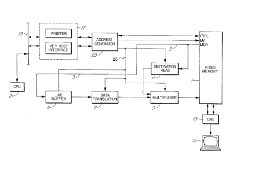
6 Figure 1 illustrates the invention in basic
7 block form. Digital signals which conform to a
8 particular color model, such as RGB or YVU are stored in
9 video memory 1, and are applied via high speed bus 3 to
a line buffer 5. Signals from line buffer 5 are applied
11 to a data translator circuit 7, which performs the
12 functions to be described below. The output signal from
13 the data translator circuit 7, referred to herein as a
14 processed source signal, is applied to a multiplexes 9.
i5 Also applied to multiplexes 9 is a destination signal,
16 read from the memory 1 by a destination signal read
17 circuit 11. The multiplexes 9 multiplexes the processed
18 source and destination signals, and produces an output
19 signal which is stored in memory 1 for further
processing, or for translation via digital to analog
21 converter 13 and for display on display 15. A
22 destination read interface circuit 11 (comprising e.g. a
23 FIFO and a data unpacker) reads destination data from
24 memory 1 and provides it to multiplexes 9.
Timing and control of the parts of the data
26 translator 7, destination read circuit and multiplexes,
27 as well as the reading of the memory 1 to read source
28 data, for providing the signals to buffer 5 is provided
29 by arbiter and host CPU interface 17. These elements
interface a main computer bus 19, such as an ISA bus, to
31 which the main CPU 21 of the computer is connected. The
32 interface connects to the arbiter, which receives
33 signals from and sends signals to the CPU 21. Arbiter
34 signals are generated in arbiter 17 for each of the
units 7, 9 and 11 to control their operation, and causes
4
21I3~~a
1 an address generator 23 to generate appropriate
2 addresses for each of the units 7, 9 and 11 to complete
3 control signals for unit 7, 9 and 11.
4 Further, CPU 21 establishes virtual
connections between the units 7, 9 and 11 by sending
6 signals via host interface of 17 to memory 1 to set up a
7 parameter list which defines the required operation
8 (such as a color-space transformation, or a scaling of
9 an image), and assigns specific trigger codes to that
parameter list. There may be any number of virtual
11 connections for any given process. Once all the virtual
12 connections have been set up, the system operates
13 independently of the CPU 21, thus relieving it from the
14 video control, and allowing it to deal with other
computer processes.
16 The system described herein triggers operation
17 of the various units by sending a specific truer code
18 assigned to that operation, via a control bus~25. When
19 any unit receives a trigger code, it locates the
parameter list assigned to that specific message, and
21 then performs the operation as defined in that parameter
22 list. All this is performed independently of the
23 computer CPU 21.
24 Parameter lists may be linked together, so
that one trigger code can trigger a number of
26 operations. Furthermore, as parameter lists exist in
27 shared memory 1 and their structure is defined to all
28 components, parameters can be altered concurrently with
29 a process.
Preferably the control bus uses a serial bus
31 protocol to facilitate event synchronization between
32 components in a multi-media computing environment. Each
33 device on the bus has an opportunity to transmit a
34 preferably 16 bit message to the other devices on the
bus .
5
21~.36~0
1 The bus requires only two pins on each device
2 to implement: clock and data. The arbiter provides a
3 stable clock and polls for requests from all devices
4 connected to the bus. Polling for requests is
accomplished by transmitting a series of "invitations";
6 one for each of the devices (addressed by ID number) on
7 the bus 25. While only one arbiter is required, any of
8 the devices could be made capable of performing the
9 function, by using appropriate circuitry.
l0 The arbiter constantly cycles through a series
il of invitations to allow each device on the bus 25 to use
12 a brief time slot for signalling other components in the
13 system. An invitation begins with a start bit and is
14 followed by a device ID signal - an "invitation to
send". All devices receive the ID signal and decode its
16 value. The device that matches the invitation ID can
17 then choose to accept the invitation by asserting an
18 invitation acknowledge bit into the bit stream.
19 Following the invitation acknowledge bit; the selected
device then broadcasts its signal event which represents
21 some form of status or message. The significance of
22 these messages is decoded by all devices on the bus 25
23 and 18 acted upon by the appropriate target device(s).
24 The arbiter cycles through all of the device IDs that
are connected so that each device has an opportunity to
26 broadcast a message. Messages or "signal events" are
27 preferably 16 bit fields containing a 4 bit function
28 code and a 12 bit data field.
29 A typical data packet, as shown in Figure 2,
begins when the arbiter transmits an invitation composed
31 of a start bit (bit 0) followed by a 3 bit invitation ID
32 (bits 1-3). It then should release the bus on cycle 4
33 leaving the bus in the de-asserted state. The device
34 with matching ID then should take over the bus and
assert an invitation acknowledge (bit 5) to indicate
6
2123000
1 that it will commence transmission of the signal event.
2 The sequence is depicted in the time bar chart below the
3 packet example.
4 With respect to Figure 3, in some cases a
signal event from the invited source requires an
6 acknowledgment from the destination or target of the
7 signal event. In this case the service acknowledge
8 signal should be driven from the target at bit location
9 22. Bit 21 is then used as a switchover time duration
for the source of the signal event to release the bus to
11 the target. Acknowledgment of a service request is
12 required since devices may have very limited (or no)
13 queuing capabilities. A true acknowledge ('1') then
14 indicates that the target of the service request either
has room in its request queue or it isn't busy
16 performing a service and can therefore accept another
17 request. When a request isn't acknowledged, the
18 requester can retry each time it is invited to use the
19 bus until the request is acknowledged.
Most of the time the bus 25 will contain only
21 circulating invitations from the arbiter with no device
22 actually accepting the invitations. In these cases the
23 Signal Event portion of the packet is skipped. It is
24 the responsibility of each device on the bus to monitor
the invitation acknowledge of each invitation to
26 determine when to begin looking for the next start bit.
27 The abbreviated packet is depicted in Figure 4.
28 It is not necessary for the arbiter to
29 circulate ID codes that are never utilized.
Consequently the arbiter could be programmable to allow
31 some ID codes to be excluded. However, this will not
32 have a large impact on worst case latency. For
33 simplicity, it is sufficient to always cycle through
34 each ID code from 0 to 7.
7
2113~~p
1 The problem of loss of synchronization can be
2 dealt with by the following. If, for example, a device
3 falsely detects a start bit then it must be able to re-
4 sync within a brief period of time. For this purpose
each bus device should monitor the bus to detect 10
6 consecutive low bits (called a "break"). Once a break
7 is detected, each device knows that the next '1' that is
8 seen is a start bit. It is for this reason that bit 14
9 of a data packet is preferably always '1' to ensure that
the data packet can never contain 10 consecutive zeroes.
11 The arbiter must insert a break after each set of 8
12 invitations to cause a re-synchronization.
13 A full data packet consists of an invitation
14 (start bit followed by an invitation ID), an invitation
acknowledge followed by a signal event. A signal event
16 consists of a 4 bit function code followed by a 12 bit
17 data field. The data field can also include an
18 acknowledgment from the start (destination) of the
19 signal event. The following table contains some of the
function code definitions that could be used:
21
22 Function Code (4 Bits) Data Field (i2 Bits)
23 Audio Record Sync 12 bit Time stamp
24 Audio Playback Sync 12 bit Time stamp
Graphics scan line count 12 bit Line number
26 Video Scan line count 12 bit Line number
27 Service Request (OxE) 10 bit service number
28 1 switch over bit (ignore
data)
29
1 bit empty or ack from
31 target device if possible
32 Service complete (OxF) 10 bit service number
33 (always paired with 1 bit (not used)
34 Service request) 1 bit service successful
8
2ii3sso
1 A service is a set of operations requested by
2 one device (the source) and performed by another (the
3 target).
4 A service request is sent by the source device
and consists of a 10 bit service number indicating one
6 of 1024 services to be performed, and a 1 bit
7 acknowledge from the target device indicating that the
8 service request was received. It is important that the
9 host CPU 21 allocate unique service numbers to each
to target so that two request receivers will not accept the
11 same service number. A service complete message should
12 be sent by the receiver of a service request to indicate
13 that it has finished processing the request. It should
14 also return a 1 bit flag indicating that the service was
performed successfully or unsuccessfully. The service
16 number it returns should be the same as the service
17 number that it received and acknowledged in the service
18 request. If a service request is received and accepted
19 by a device then it should return a completion message
at some later time.
21 A preferred embodiment of the invention is
22 shown in detailed block diagram as illustrated in
23 Figures 5 and 6, which should be assembled together as
24 illustrated in Figure 7. It should be understood that
the various signal variables which will be shown as
26 inputs to the various circuits are obtained from data
27 decoded by bus interface circuits in each of the devices
28 connected to the bus, which recognize the ID signals
29 referred to above, receive packets designated for the
circuits, and obtain the variable signals as data in the
31 packets. The interface circuits would be known to a
32 person skilled in the art, and thus will not be
33 described; their designs do not form part of this
34 invention.
9
2z~3soo
1 Video signals in e.g. RGB or YCrCb models are
2 received or are transmitted (by an I/O interface to a
3 high speed bus connected to memory 1, not shown) to
4 scales 531.
Scales circuit 531 receives source signals
6 pixel data via source bus 532 from the memory bus. A
7 destination bus 533 carries an output signal from the
8 scales to the color conversion unit.
9 The structure is comprised of an ALU 539 for
performing a vertical blend function and an ALU 541 for
11 performing a horizontal blend function. ALU 539
12 receives the vertical blending coefficients a~ and b~
13 and the vertical accumulate Accv flag.
14 Similarly, the ALU 541 receives from screen
memory, via the data portion of the packet described
16 earlier, the horizontal blend coefficients aH and bH and
17 the accumulate AccH flag. The Acc bits determine whether
18 R should be added or zero should be added. Acc is a
19 flag specified in the coefficient list.
ALU 539 receives adjacent pixel data relating
21 to the first or input trajectory on input ports Q and P,
22 the data for the Q port being received via line buffer
23 543 from the data source, which can be the screen
24 memory, via source bus 532. The output of line buffer
543 is connected to the input of line buffer 545 via
26 multiplexes 562, the output of line buffer 545 being
27 connected to the P port of ALU 539.
28 The output of ALU 539 is applied to the input
29 of pixel latch 560. The Q pixel data is applied from
the output of ALU 539 to the Q input port of ALU 541 and
31 the P pixel data is applied from the output of pixel
32 latch 560 to the P input port of ALU 541. The P pixel
33 data is also applied to the other input of multiplexes
34 562.
~~ °~~dn
1 The output of ALU 541 is applied to the input
2 of pixel accumulator 549, which provides an output
3 signal on bus 533 for application to a color conversion
4 unit.
The line buffers are ideally the maximum
6 source line size in length. The accumulator values Accv
7 and AccH applied to ALU 539 and ALU 541 respectively
8 determine whether R should be forced to zero or should
9 equal the value in the accumulator.
In operation, a first line of data from a
11 source trajectory is read into line buffer 543. The
12 data of line buffer 543 is transferred to line buffer
13 545, while a second line of data is transferred from the
14 source trajectory to the line buffer 543. Thus it may
be seen that the data at the P and Q ports of ALU 539
16 represent pixels of two successive vertical lines.
17 Thus the output of the vertical blend ALU 539
18 is applied directly to the Q port of the horizontal
19 blend ALU 541, and the output of vertical blend ALU 539
is also applied through a pixel latch 560 to the P port
21 of ALU 541. The output of line buffer 543 is connected
22 to the input of a multiplexer 562; the output of pixel
23 latch 560 is connected to another input of multiplexer
24 562. The Accv input is connected to the control input
of multiplexer 562. The output of multiplexer 562 is
26 connected to the input of line buffer 545.
27 The vertical blend ALU 539 can only accumulate
28 into the line buffer 545. The blend equation becomes
29
3o a"P+bvQ P
16
31
32 wherein the result of the equation is assigned back to P
33 if a vertical accumulate is desired.
11
2~~3fi~~
1 For the rest of each horizontal line the data
2 relating to two consecutive horizontal pixels are
3 applied on input lines Q and P to ALU 541 and are
4 blended in accordance with the equation
aHpl(bxQ +R -~ R
8 The result of this equation is output from ALU
9 541 and is stored in pixel accumulator 549.
l0 The pixel data is transferred from line buffer
11 543 into line buffer 545. The source trajectory is read
12 and transferred to line buffer 543. The steps described
13 above for the vertical blending function is repeated for
14 the rest of the image.
Coefficient generation in the vertical
16 direction should be modified accordingly. Line buffer
17 545 is otherwise loaded whereby line buffer 543 data is
18 transferred to it only when the source Y increment bit
19 is set.
Smaller line buffer sizes, i.e. only 32 pixels
21 strains the maximum source width, but has no effect on
22 source height. Thus if the source width is greater than
23 32 pixels, the operation can be sub-divided into strips
24 of less than 32 pixels wide. Since this may affect
blending, the boundaries of these divisions should only
26 occur after the destination has been written out (i.e. a
27 horizontal destination increment). With a maximum
28 stretch/reduce ratio of 16:1, the boundary thus lands
29 between 16 and 32 pixels in the X direction. The
coefficients at the boundary conditions should be
31 modified accordingly.
32 In a successful prototype of the invention 32
33 pixel line buffers and a 128 element X coefficient cache
12
2~~36~~
1 were used. Y coefficients are not cached and were read
2 on-the-fly. The embodiment is preferably pipelined,
3 i.e. each block may proceed as soon as sufficient data
4 is available.
It should be noted that the source trajectory
6 should only increment with a source increment that is
7 set in a coefficient list in the screen memory or
8 equivalent. If the source is incremented in the X
9 direction and not in the Y direction and the end of the
source line is reached, the source pointer is preferred
11 to be reset to the beginning of the current line. If
12 the source is incrementing in both directions and the
13 end of the source line is reached, it is preferred that
14 the source pointer should be set to the beginning of the
next line.
16 The destination trajectory should be
17 incremented in a similar fashion as the source
18 trajectory except that the destination increment bits of
19 the coefficient list should be used.
Line buffer pointers should be incremented
21 when the source increment bit is set in the X direction.
22 They should be reset to zero when the end of the source
23 line is reached. Data should not be written to line
24 buffer 543 nor transferred to line buffer 545 if the
source increment bit is not set in the Y direction.
26 Destination data should only be written out from the
27 pixel accumulator if both X and Y destination increments
28 bits are set.
29 The X coefficient pointer in the screen memory
should be incremented for each horizontal pixel
31 operation, and the Y coefficient pointer should be
32 incremented for each line operation.
33 The design described above which performs the
34 vertical pixel blending prior to the horizontal pixel
blending is arbitrary, and may be reversed in which
13
211360
1 horizontal blending is performed prior to vertical
2 blending. It should be noted that blending in only one
3 direction can be implemented, whereby one of the ALUs is
4 provided with coefficients which provide unitary
transformation, i.e. neither expansion nor contraction
6 of the image.
In a successful prototype of the invention 532
8 pixel line buffers and a 128 element X coefficient cache
9 were used. Y coefficients are not cached and were read
on-the-f ly .
11 The output of pixel accumulator 549 is applied
12 via bus 533 to the input of a color space converter.
13 This signal is typically comprised of three input signal
14 components AinBinCin. The input signals are applied to
clippers 417, 418 and 419 respectively.
16 Also applied to each of the clippers 417, 418
17 and 419 are ceiling and floor limit data signals or
18 values which establish ranges within which the input
19 signal components should be contained.
When the input signals exceed, either
21 positively or negatively, the limits designated by the
22 ceiling or floor values, the respective signal component
23 is saturated (clipped) to the ceiling or floor (upward
24 or downward limit) respectively.
The output signals of the clippers are applied
26 to respective inputs of a matrix multiplier 421, in the
27 preferred embodiment a [3x3]x[3x1) matrix multiplier.
28 Also input to the multiplier is an array 423 of
29 parameter data which forms a color transformation
matrix. The transformation performed in the matrix
31 multiplier will be described below.
32 The three outputs of the matrix multiplier 421
33 are applied to three inputs of a vector adder 425. A
34 3x1 array 427 of parameters is input to vector adder
425, which performs the function [3x1]+[3x1], as will be
14
1 described below. The parameters Ox in the array 427
2 constitute offset vectors.
3 The three outputs of vector adder 425 are
4 applied to respectively inputs of output clippers 429,
430 and 431 to which ceiling and floor limit data
6 signals are applied. The output clippers operate
7 similarly to the input clippers 417, 418 and 419,
8 ensuring that the output signal components are contained
9 within the range defined by the output ceiling and floor
limits, and if the output signal components exceed those
il limits, they are clipped (saturated) to the ceiling and
12 floor levels. The resulting output signals from
13 clippers 429, 430 and 431, designated by Rout, Bout~ and
14 Cout constitute the three components of the output
signal in either RGB or YCrCb format.
16 In a preferred embodiment, each of the R, G
17 and B signals are equal or greater to zero and equal or
18 smaller than 255 units, the Y component is equal to or
19 larger than 16 and equal or smaller than 235, and the Cr
and Cb components are equal to or larger than 16, or
21 equal to or smaller than 240.
22 To convert from YCrCb to RGB, the matrix
23 multiplier 421 and vector adder 425 should perform the
24 following transformation:
26 R = 1.1636*(Y-16)+1.6029*(Cr-128)
2~ G = 1.1636*(Y-16)-0.8165(Cr-128)-0.3935(Cb-128)
2g B = 1.1636*(Y-16)+2.0261(Cb-128)
29
To convert from RGB to YCrCb format, the
31 multiplier and adder should perform the following
32 transformations:
21~.~~~~
1 Y = +0.25708+0.50456+0.0980B+16
2 Cr = 0.43738-0.36626-0.07118+128
3 Cb = -0.14768-0.28976+0.43738+128
4
For brightness, contrast, color saturation and
6 hue control for a YCrCb signal, the input signal is
7 YCrCb and the output is YCrCb, and the following
8 transformations should be performed in the matrix
9 multiplier and adder:
to
11 Y = Y in*Contrast+Brightness
12 Cr = color-sat*(cos(hue)*(Cr_in-
13 128)+sin(hue)*(Cb-in-128))+128
14 Cb = color-sat*(-sin(hue)*(Cr-in-
128)+cos(hue)*(Cb_in-128))+128
16
17 The conversion from a YCrCb to a RGB signal
18 can be expressed in the following matrix form.
R 1.16361.6029 0.0000 Y -223.8
19 G = 1.1636-0.8165-0.3939Cr 136.3
+
B 1.16360.0000 2.0261 Cb -278.0
21 or more precisely
22 RGB = Wy~rYCrCb+OY~r
23 where W is the color transformation matrix and O is the
24 of f set vector .
The matrix multiplication step is performed in
26 the matrix multiplier 421 and the addition step is
27 performed in the vector adder 425. The RGB elements
28 constitute the values of the signal components in the
29 input signal, and the numerical parameters in the 3x3
matrix constitute the WX transformation parameters,
16
211300
1 while the values in the 3x1 matrix constitute the offset
2 vector O.
3 For conversion from an RGB to YCrCb format,
4 the transformation that should be performed in the
matrix multiplier and vector adder is
Y 0.2570 0.5045 0.0980 R 16
Cr 0.4373 -0.36620.0711 G 128
Cb -0.1476 -0.28970.4373 B 128
7
8 or more concisely
9 YCrCb = Wr~yRGB + Orgy
For brightness, contrast, color saturation and
11 hue control in a YCrCb type signal, the input signal is
12 YCrCb and the output signal is YCrCb. The matrix
13 multiplier and vector adder should perform the following
14 transformation.
Y"~ Contrast0.0000 0.0~ Y,
Cro~ 0.0000 color _ sat* color _ sat * Cr;
cos(hue) sin (hue)
Cro,~ 0.0000 -color _ sat color _ sat * Cb;
* sin(hue) cos(hue)
16
Brightness
17 128.*(1-color_sat*(cos(hue) +sin(hue)))
128* (1- color _sat* (cos(hue) - sin(hue)))
is
19 YCrCbout-Wy>yYCrCbin+Oy>y
21 In summary, for brightness, contrast, color
22 saturation and hue control when converting from a YCrCb
23 format to RGB, the transformation can be reduced to
24 RGB = Wy>r*(Wy>y*YCrCb+Oy>y)+oy>r
17
~113fi0a
1 For brightness, contrast, color saturation and
2 hue control when converting from an RGB signal to a
3 YCrCb type signal, the following reduced transformation
4 is performed.
YCrCb = Wy>y* (Wr>y*RGB+Or>y) +Oy>y
6 For performing brightness, contrast, color
7 saturation and hue control in an RGB signal, both the
8 input and output signals are in RGB format. The
9 transformation performed in the multiplier and vector
adder in reduced form is
11 RGBout=Wy>r*(Wy>y*(Wr>y*RGBin+Or>y)+Oy>y)+Oy>r
12 As noted above, the clippers 417 to 419 and
13 429-431 ensure that all data passing through them must
14 be within the ranges specified. However if the input
data is already between the specified ranges, the
16 clippers may be deleted.
17 The three outputs of the matrix multiplier are
18 respectively:
19
Ain o=Ain*W11+Bin*W21+Cin*W31
21 Bin o=Ain*W12+Bin*W22+Cin*W32
22 Cin o=Ain*W13+Bin*W2g+Cin*W33
23 The three outputs of the vector adder are
24 Aout o=Aout_i+O1
Bout o=Bout-i+02
26 Cout o=Cout-i+03
27 All arithmetic is preferably performed on 10
28 bit wide signed integer data (1 bit sign, 1 bit integer
29 and 8 bits fractional). This should be used under
normal circumstances. However if over saturation, over
31 contrast, or over brightness is desired, more integer
32 bits may be rquired, increasing the number of total data
33 bits and widening all other data paths. Floor and
34 ceiling parameters on incoming and outgoing data
18
2I~3600
1 channels are preferably 8 bits wide, and all other data
2 paths are preferably 10 bits wide.
3 Preferred integer parameter sets for each
4 respective operation are listed below. The dynamic
range of Cr and Cb have been adjusted slightly such that
6 all coefficients fall in the range [-512,+512).
7 For YCrCb to RGB conversion:
298/256 404/256 0
Wy" = 298/256 -206/256 -99/256
298/256 0 511/256
-220
Oy" _ +136
-278
9
10The floor and
ceiling parameters
for the clipping
11registers preferably
are:
12
13A in ceil 235
14A in floor 16
15B in ceil 240
16B in f loor 16
17C in-ceil 240
lgC in floor 16
19A out ceil 255
20A out floor 0
21B out ceil 255
22B out floor 0
23C out ceil 255
24C out floor 0
25
19
~~~~~oo
1 For RGB to YCrCb conversion:
66 / 129 25 /
256 / 256 256
W, 114 / -95 -18
~, 256 / 256 / 256
=
-38 / -75 114
256 / 256 / 256
2
16
O, ~ =128
128
3
4 The floor and ceiling parameters for the
clipping registers preferably
are:
6 A in ceil 255
A in floor 0
g B in ceil 255
g B in floor 0
10C in-ceil 255
11C in f loor 0
12A out ceil 235
13A out f loor 16
14B out ceil 240
15B out floor 16
16C out ceil 240
1~C out_f loor 16
18
19 For brightness, contrast, color saturation and
20 hue control of YCrCb = >YCrCb:
21~3~~0
contrast o 0
Wy" = 0 color-sat * cos(hue) color-sat * sin(hue)
0 -color-sat * sin(hue) +color-sat * cos(hue)
1
Brightness
Oy" = 128 * (1- color-sat(cos(hue) + sin(hue)))
128 * (1- color-sat * (cos(hue) - sin (hue)))
2
3 The floor and ceiling parameters for the
4 clipping registers preferably are:
A in ceil 235
6 A in floor 16
7 B in ceil 240
8 B in floor 16
9 C in-ceil 240
C in floor 16
11 A out ceil 235
12 A out floor 16
13 B out ceil 240
14 B out floor 16
C out ceil 240
16 C out floor 16
17
18 For brightness, contrast, color saturation and
19 hue control of YCrCb=>RGB:
W=Wy>r*Wy>y
21 O=WY~r*Oy~Y+Oy>r
22 The clipping registers are set as with
23 straight YCrCB to RGB conversion.
24 For brightness, contrast, color saturation and
hue control of RGB=>YCrCb:
21
1 W=WY>Y*Wr>Y
2 p-Wy>y*pr>y+Oy>y
3 Clipping registers are set as with straight
4 RGB to YCrCb conversion.
For brightness, contrast, color saturation and
6 hue control in RGB=>RGB:
7 W-Wy>r*Wy>y*Wr>y
g p=Wy>r*~Wy>y*pr>y+Oy>y)+Oy>r
9 The floor and ceiling parameters for the
l0 clipping registers preferably are:
11 A in ceil 255
12 A in floor 0
13 B in ceil 255
14 B in floor 0
15 C in-ceil 255
16 C in f loor 0
1~ A out ceil 255
lg A out floor 0
19 B out ceil 255
20 B out floor 0
21 C out ceil 255
22 C out floor 0
23
24 It is preferred that all matrix
25 multiplications should be performed in floating point
26 and only converted to integer just before loading the
27 coefficients to the hardware color conversion unit.
28 This minimizes transformation error.
29 It should be noted that the input clipping
30 parameters and output clipping parameters are preferably
31 programmable. Thus any three component number set may
32 be transformed into any other three component set as
33 long as that transformation is linear. In particular,
34 any three component color model may be transformed to
35 any other three component color model as long as that
22
1 transformation is linear. If the multipliers and data
2 paths were widened, it would be practical to perform
3 other useful transformations, such as xyz coordinate
4 transformation for example.
The output of the color space conversion
6 circuit is input to an output multiplexer 620. Source
7 data is data relating to a video or graphical signal
8 which is to be mixed with destination pixel data (or in
9 short, simply destination data). Destination data is
data already in the memory 1 which is to be displayed,
11 and can result from another source such as a video
12 input, in a manner known in the art.
13 It is preferred that the source data should be
14 passed through an output masking gate 623. The output
masking gate 623 should be always enabled, although it
16 may be set such that it does not mask anything.
17 The output multiplexer 620 has a control input
18 621 to which a keying signal is applied. Thus depending
19 on the value of the keying signal, a pixel of either
destination data or source data is provided at the
21 output 622 of the multiplexer 620. Data at the output
22 622 is written to the destination memory, which can be a
23 destination register or the memory 1.
24 The destination and source data is also
provided to inputs of an input multiplexer 24. A mode
26 signal applied to a control input 625 of multiplexer 624
27 selects which of the signals, a pixel of either
28 destination or source, will be provided at its output,
29 from which the keying signal, if provided for that
pixel, will be derived. The mode signal can be a bit
31 provided to the mixing unit from a control register of
32 the display processor.
33 Various components of data defining each pixel
34 (7:0, 15:8, 23:16 and/or 31:24) are then individually
passed through respective gates 627, 628, 629 and 630,
23
1 each of which receives 8 mask bits IMASK from a control
2 register of the display processor. This provides a
3 means to mask off bits which will not participate in
4 generating the keying signal, and thus to inhibit
keying. OMASK and IMASK are preferably 32 bits wide,
6 corresponding to the four 8 bit pixel components that
7 are being operated upon. Since each of the components of
8 data can define a particular characteristic of the
9 pixel, e.g. color, embedded data, exact data, etc., this
provides a means to inhibit or enable keying on one of
11 those characteristics, or by using several of the
12 components and masking switches, to inhibit or enable
13 keying based on a range of colors, embedded data, etc.
14 The outputs of each of the gates 627, 628,
629, 630 is applied to one input of each of pairs of
16 comparators 633A and 6338, 634A and 6348, 635A and 6358,
17 and 636A and 6368. Data values A and B are applied via
18 masking gates 638A and 6388, 639A and 6398, 640A and
19 6408, and 641A and 418 respectively to the corresponding
respective inputs of the comparators 633A - 636B. The
21 same masking bits IMASK that are applied to the gates
22 627 - 630 are applied to the respective corresponding
23 gates 638A - 418. The data values A and B are static,
24 and are masked by the gates in a similar manner as the
destination or source data. Compare function selection
26 signals FNA1, FNB1; FNA2, FNB2; ... - FNB4 are applied
27 to select the compare function of the corresponding
28 gates 633A - 6368.
29 Each pair of comparators compares each 8 bit
pixel component with two values, the respective masked
31 pixel components from value A and from value B. Each
32 component has a separate compare function with each of
33 the two comparison values.
34 The result of all of the component comparisons
with the A value are ANDed together in AND gate 643, and
24
21I36~~
1 the result of all of the component comparisons with the
2 B value are ANDed together in AND gate 645. The outputs
3 of AND gates 643 and 645 are applied to logic circuit
4 647. A CSelect bit from a control register of the
memory 1 is applied to a control input of logic circuit
6 647, to determine whether the results output from AND
7 gates 643 and 645 should be ANDed or ORed together.
8 The output of logic circuit 647 is the keying
9 signal. It is applied to control input 621 of the
output multiplexer, preferably through inverter 649. A
li signal ISelect applied from a control register of the
12 memory 1 processor to a control input of inverter 649
13 determines whether the keying signal should be inverted
14 or not. This provides means to inverse key on the data,
e.g. to instantly switch the other of the destination or
16 source data as the keyed data into or around a keying
17 boundary merely by implementing a 1 bit software switch
18 command ISelect.
19 Thus if the key signal data is FALSE,
destination data is output from multiplexer 620. If the
21 key signal is TRUE, the source data is masked with the
22 output mask 623 and written to the destination.
23 The state of the mixing unit can be programmed
24 by the following configuration, which can be stored in
control or configuration registers:
2~~3sas
1 Register Number
2 Name of
Bits
Description
3
4 Mode 1 Selects either the source ion
or destinat
for comparison.
6 CSelect 1 Selects AND or OR the results A
of the
and B comparisons.
8 ISelect 1 Sects INVERT or no operation.
9 ValueA 32 Value A to compare.
ValueB 32 Value B to compare.
11 IMask 32 Input mask for masking off bits which
12 will not participate in the n.
compariso
13 OMask 32 Output mask for preventing bits from
14 being overwritten at the
destination.
FNA1 3 Compare function for pixel component 1
16 and value A.
17 FNA2 3 Compare function for pixel component 2
lg and value A.
19 FNA3 3 Compare function for pixel component 3
and value A.
21
22 FNA4 3 Compare function for pixel component 4
23 and value A.
24 FNB1 3 Compare function for pixel component 1
and value B.
26 FNB2 3 Compare function for pixel component 2
2~ and value B.
28 FNB3 3 Compare function for pixel component 3
29 and value B.
FNB4 3 Compare function for pixel component 4
31 and value B.
32
33
26
21.~.36~~
1 The eight possible comparison functions are
2 the following:
3
4 Function Number Description
000 False
7 001 True
g 010 Data>=Value
9 011 Data<Value
100 Data!=Value
11 101 Data==Value
12 110 Data<=Value
13 111 Data>Value
14
In the embodiment illustrated, four groups of
16 bits, bits 0 - 7, bits 8 - 15, bits 16 - 23, and bits 24
17 - 31, defining four components of a single pixel, are
18 separately processed, giving a very high degree of
19 flexibility in keying. These four components can define
the red, green and blue (RGB) color of a picture or can
21 be each of the Y,U,V parameters for that type of
22 picture. The fourth component is provided for in case a
23 destination compare operation is desired to be
24 performed. This fourth component is referred to as the
alpha channel, and is usable by the application
26 software.
27 However it will be noted that in some cases
28 four, or three (if the alpha channel is not used),
29 components need not be used. In a simpler system, such
3o as a monochrome system, or in a system in which a color
31 signal is to be processed by the use of only one
32 component, only one mask 627, one pair of comparators
33 633A and 633B, and one pair of masks 638A and 638B can
34 be used. AND gates 643 and 645 can then be dispensed
with and the outputs of comparators 633A and 633B can be
36 applied directly to inputs of logic circuit 647.
27
~1~36a~1
1 Figure 8 illustrates the type of result that
2 use of the pre invention can provide. A full screen
'~~ 3 graphic screen /651 can contain multiple overlapping full
~~'C~ ~~, 4 motion video streams Video 1, Video 2, and Video 3.
The live video windows may be partially
6 obsured by other windows. To deal with odd clip
7 regions, the program application software should assign
8 an ID to each of the distinct regions: graphics, Video
9 1, Video 2, and Video 3. This ID should then be written
to the alpha channel of each pixel in the destination.
11 Each video source should then be keyed to its own ID
12 using the mixing unit described above, so that writing
13 is inhibited outside it's own region.
14 To implement this, and assuming that the alpha
channel has been set up (channel 4, bits 0 - 7), the
16 data provided from the control registers to the various
17 control inputs described above, i.e. one possible video
18 mixer configuration can be:
19 Register Value
21 Mode DESTINATION
22 CSelect OR
23 ISelect No operation
24 ValueA REGION ID
ValueB don't care
26 IMask OOOOOOFF
2~ OMask FFFFFF00
2g FNA1 TRUE
29 FNA2 TRUE
FNA3 TRUE
31 FNA4 Data==ValueA
32 FNB1 FALSE
33 FNB2 FALSE
34 FNB3 FALSE
FNB4 FALSE
36
3~ A possible video mixer configuration to mix
38 two video streams, one of which is blue screened to
39 provide for video special effects) is as follows. The
28
2113600
1 non-blue screened source may also be a computer
2 generated background.
3 Register Value
4 Mode Blue-screened data is SOURCE
CSelect AND
6 ISelect INVERT
ValueA Lower color bound
g ValueB Upper color bound
9 IMask FFFFFF00
OMask FFFFFF00
11 FNA1 Data>ValueA
12 FNA2 Data>ValueA
13 FNA3 Data>ValueA
14 FNA4 TRUE
FNB1 Data<ValueB
16 FNB2 Data<ValueB
1~ FNB3 Data<ValueB
lg FNB4 TRUE
19
Register Value
21
22 Mode Blue-screened data is
23 DESTINATION
24 CSelect AND
ISelect No operation
26 ValueA Lower color bound
2~ ValueB Upper color bound
2g IMask FFFFFF00
29 OMask FFFFFF00
FNA1 Data>ValueA
31 FNA2 Data>ValueA
32 FNA3 Data>ValueA
33 FNA4 TRUE
34 FNB1 Data<ValueB
FNB2 Data<ValueB
36 FNB3 Data<ValueB
3~ FNB4 TRUE
38
39 To overlay computer graphics or text on top of
a video stream or graphical image, the following
41 possible video mixer configuration can be used. It
42 should be noted that this is similar to blue screening,
43 except that the computer graphics signal is used to key
44 on a specific color.
46
29
21I36~a
1 Rectister Value
Mode Graphics data is SOURCE
2 CSelect OR
3
4 ISelect INVERT
g ValueA Color Key
ValueB Don't care
7 IMask FFFFFF00
g OMask FFFFFF00
FNA1 Data==ValueA
g FNA2 Data==ValueA
FNA3 Data==ValueA
11 FNA4 TRUE
12
13 FNB 1 TRUE
14 FNB2 TRUE
FNB3 TRUE
16 FNB4 TRUE
17
lg Register Value
19
Mode Graphics data is DESTINATION
CSelect OR
21
22 ISelect No operation
23 ValueA Color Key
24 ValueB Don't care
IMask FFFFFF00
26 OMask FFFFFF00
27 FNA1 Data==ValueA
FNA2 Data==ValueA
2g FNA3 Data==ValueA
29 FNA4 TRUE
31 FNB 1 TRUE
32 FNB2 TRUE
33 FNB 3 TRUE
34 FNB4 TRUE
36 A person skilled in the art understanding this
37 invention may now design variations or other
38 embodiments, using the principles described herein. All
39 such variations or embodiments are considered to fall
within the scope of the claims appended hereto.