Note: Descriptions are shown in the official language in which they were submitted.
_ 21 1 3606
1
TRANSVERSAL FILTER CAPABLE OF PROCESSING
AN INPUT SIGNAL OF HIGH DATA RATE
Background of the Invention:
This invention relates to a transversal filter for
use in a waveform equalization circuit in a digital communi-
cat ion system and, more part icularly, to a t ransversal f i lter
of a parallel processing type.
In general, the transversal filter is used in a
waveform shaping filter such as the waveform equalization
circuit in the digital communicat ion system or an interference
canceller. The transversal filter has been digitized and put
to practical use due to miniaturization of the device) low
power consumption, and ad~ustmentless. In addition, in order
to be operable at a high speed, it has been made a proposal to
make a plurality of transversal filters process in parallel to
construct the transversal filter of the parallel processing
type. Such a transversal filter of the parallel processing
type has been disclosed, for example, in Canadian Patent
2,007;922 dated July 7, 1993.
A conventional transversal filter is supplied with
an input signal having an input data rate. The input signal
may be a baseband digital signal which is obtained by
demodulating and decision a digital modulated
64768-306
t.:
~i~3so~
2
signal. The transversal filter filters the input signal
into an output signal in response to first through J-th
tap gains, where J represents a first positive integer
which is not less than two. The output signal also has
an output data rate equal to the input data rate. The
transversal filter comprises a delay circuit which has
first through J-th taps. The input signal is supplied to
the delay circuit. The delay circuit comprises first
through (J-1)-th delay units each of which is placed
between two taps of the first through the J-th taps.
Each of the first and the (J-1)-th delay units provides a
unit delay which is substantially equal to a reciprocal
of the input data rate. The first through the J-th taps
of the delay circuit produce first through J-th tap
signals, respectively.
The first through the J-th tap signals are
supplied to first and second latch circuits. The first
latch circuit latches the first through the J-th tap
signals at each odd time slot of the input signal and
holds these signals during a time duration corresponding
to two time slots to produce first through J-th primary
latched signals. Likewise, the second latch circuit
latches the first through the J-th tap signals at each
even time slot of the input signal and holds these
signals during the time duration corresponding to the two
time slots to produce first through J-th subsidiary
latched signals.
2113~0~
The first through the J-th primary latched
signals are supplied to a first calculation circuit. The
first calculation circuit comprises first through J-th
primary multiplying circuits and a first adding circuit.
The first through the J-th primary multiplying circuits
are supplied with the first through the J-th primary
latched signals. The first through the J-th tap gains
are supplied to the first through the J-th primary
multiplying circuits, respectively. The first through
the J-th primary multiplying circuits multiplies the
first through the J-th primary latched signals by the
first through the J-th tap gains to produce first through
J-th primary product signals, respectively. The first
through the J-th primary product signals are supplied to
the first adding circuit. The first adding circuit adds
up J terms of the first through the J-th primary product
signals to produce a first addition result signal
indicative of a first addition result of the J terms.
Likewise, the first through the J-th subsidiary
latched signals are supplied to a second calculation
circuit. The second calculation circuit comprises first
through J-th subsidiary multiplying circuits and a second
adding circuit. The first through the J-th subsidiary
multiplying circuits are supplied with the first through
the J-th subsidiary latched signals. The first through
the J-th tap gains are supplied to the first through the
J-th subsidiary multiplying circuits, respectively. The
first through the J-th subsidiary multiplying circuits
4 2~~3fi~fi
multiply the first through the J-th subsidiary latched
signals by the first through the J-th tap gains to
produce first through J-th subsidiary product signals,
respectively. The first through the J-th subsidiary
product signals are supplied to the second adding
circuit. The second adding circuit adds up J terms of
the first through the J-th subsidiary product signals to
produce a second addition result signal indicative of a
second addition result of the J terms.
The first and the second addition result signals
are supplied to a parallel-serial converter. The
parallel-serial converter carries out a parallel-serial
conversion on or couples the first and the second
addition result signals to produce a serial converted
signal as the output signal.
As apparent from the above description, the
transversal filter produces the output signal which is
equalized thereby. In the conventional transversal
filter, the first and the second latch circuits
distribute input elements of the input signal into the
first through the J-th primary latched signals and the
first through the J-th subsidiary latched signals at
alternative timings. In other words, each of the first
and the second latch circuits serves as a serial-parallel
converter for converting the input signal into J latched
signals each of which has a data rate equal to a half
times as large as the input data signal of the input
signal. Accordingly, the first and the second
2~~3fi~~
calculation Circuits carry out the parallel processing at
a low operational speed which is equal to a half of the
output data rate of the output signal. However, each of
the first through the (J-1)-th delay units must carry out
a delay operation at an operational speed equal to the
input data rate of the input signal. As a result, the
conventional transversal filter is defective in that the
input data rate of the input signal and the operational
speed of the transversal filter are restricted by the
operational speed of the first through the (J-1)-th delay
units.
Summary Qf the Invention:
It is therefore an object of this invention to
provide a transdersal filter capable of processing an
input signal of high data rate.
It is another object of this invention to provide
a transversal filter of the type described, which is
operable at a high speed.
Other objects of this invention will become clear
as the description proceeds.
On describing the gist of an aspect of this
invention, it is possible to understand that a
transversal filter filters an input signal into an output
signal in response to first through J-th tap gains, where
J represents a first positive integer which is not less
than two. The input signal has an input data rate while
the output signal has an output data rate which is equal
to the input data rate.
2~~3~06
According to the above-mentioned aspect of this
invention, the above-understood transversal filter
comprises a serial-parallel converter, supplied with the
input signal, for converting the input signal into first
through M-th parallel converted signals, where M
represents a second positive integer which is not less
than two. Connected to the serial-parallel converter, a
delay circuit has first through L-th taps, where L
represents a third positive integer which is greater than
the first positive integer J. The delay circuit
comprises a plurality of delay units each of which is
connected between two taps selected from the first
through the L-th taps. Each of the delay units provides
M times a unit delay which substantially equal to a
reciprocal of the input data rate. The first through the
L-th taps of the delaying circuit produce first through
L-th tap signals, respectively. Each of first through
M-th calculation circuits is supplied with the first
through the J-th tap gains and J tap signals selected
from the first through the L-th tap signals. The first
through the M-th calculation circuits carry out a
calculation operation on the J tap signals using the
first through the J-th tap gains to produce first through
M-th calculation result signals, respectively. Connected
to the first through the M-th calculation circuits, a
coupling circuit couples the first through the M-th
calculation result signals to produce the output signal.
~7
On describing the gist of a different aspect of
this invention, it is possible to understand that a
transversal filter filters an input signal into an output
signal in response to first through J-th tap gains, where
J represents a first positive integer which is not less
than two. The input signal has an input data rate while
the output signal has an output data rate which is equal
to a half of the input data rate.
According to the different aspect of this
invention, the afore-understood transversal filter
comprises a serial-parallel converter, supplied with the
input signal, for converting the input signal into first
through M-th parallel converted signals, where M
represents a second positive integer which is not less
than two. Connected to the serial-parallel converter, a
delay circuit has first through L-th taps, where L
represents a third positive integer which is greater than
the first positive integer J. The delay circuit
comprises a plurality of delay units each of which is
2p connected between two taps selected from the first
through L-th taps. Each of the delay units provides M
times a unit delay which substantially equal to a
reciprocal of the input data rate. The first through
L-th taps of the delaying circuit produce first through
L-th tap signals, respectively. Each of the first
through M-th latch circuits is supplied with J tap
signals selected from the first through the L-th tap
signals. Each of the first through the M-th latch
2~i3~~~
circuits latches the J tap signals and holding the J tap
signals during a time duration which substantially equal
to twice a reciprocal of the output data rate to produce
first through J-th latch signals. First through M-th
calculation circuits are connected to the first through
the M-th latch circuits, respectively. Each of the first
through the M-th calculation circuits is supplied with
the first through the J-th tap gains. The first through
the M-th calculation circuits carrying out a calculation
operation on the first through the J-th latch signals
using the first through the J-th tap gains to produce
first through M-th calculation result signals,
respectively. Connected to the first through the M-th
calculation circuits, a coupling circuit couples the
first through the M-th calculation result signals to
produce the output signal.
Brief Description of the Draping:
Fig. 1 is a block diagram of a conventional
transversal filter;
Fig. 2 shows a time chart for use in describing
an operation of the conventional transversal filter
illustrated in Fig. 1;
Fig. 3 is a block diagram of a transversal filter
. according to a first embodiment of this invention;
Fig. 4 shows a time chart for use in describing
an operation of the transversal filter illustrated in
Fig. 3;
~~~~606
9
Fig. 5 is a block diagram of a transversal filter
according to a second embodiment of this invention;
Fig. 6 shows a time chart for use in describing
an operation of the transversal filter illustrated in
Fig. 5;
Fig. 7 is a block diagram of a modified
serial-parallel converter into which a serial-parallel
converter fdr use in the transversal filter illustrated
in Fig. 3 is modified; and
Fig. 8 shows a time chart for use in an operation
of the modified serial-parallel converter illustrated in
Fig. 7.
Description of the Preferred Embodiments:
Referring to Fig. 1, a conventional transversal
filter of a parallel processing type will be described
at first in order to facilitate an understanding of the
present invention. The illustrated transversal filter
is a three-tap transversal filter supplied with an
input signal IN'. In the example being illustrated,
the input signal IN has an input data rate and is a
digital signal having waveform shaped. The input
signal IN may be a baseband digital signal which is
obtained by demodulating and decision a digital modulated
signal which is transmitted at a predetermined modulation
rate.
The three-tap transversal filter filters the
input signal IN into an output signal OUT in response to
first through J-th controllable tap gains, where J
10
represents a first positive integer which is not less
than two. In the example being illustrated, the first
positive integer J is equal to three and the three-tap
transversal filter therefore responds to the first
through the third tap gains which may be specified by
C_1, C0, and Cl. The output signal OUT has an output
data rate equal to the input data rate. The three-tap
transversal filter comprises a delay circuit 10' which
has first through third taps 11', 12', and 13'. The
second tap 12' may be called a central tap. The first
and the third taps 11' and 13' are depicted on the
lefthand and the righthand sides of the central tap 12'.
The first and the third taps 11' and 13' may be referred
to as first and second additional taps.
The input signal IN is supplied to the delay
circuit 10'. The delay circuit 10' comprises first and
second delay units 16' and 17' which are placed between
the first and the second taps 11' and 12' and between the
second and the third taps 12' and 13', respectively.
Each of the first and the second delay units 16' and 17'
provides a unit delay which is substantially equal to a
reciprocal of the input data rate. The input signal IN
is delivered to the first tap 11' as a first tap signal
and successively delayed by the first and the second
delay units 16' and 17' to be produced as second and
third tap signals which are sent to the second and the
third taps 12' and 13', respectively.
11
Let the first through the third taps 11', 12',
and 13' be specified by consecutive numbers of (-1), 0,
and (+1), respectively, taking the successive delays into
consideration. In this connection, the first tap signal
appearing as the (-1) tap 11' may be specified by Dn+1'
Likewise, the second and the third tap signals may be
specified by Dn and Dn-1, respectively. Since the first
tap signal Dn+1 is identical with the input signal IN
with no delay, it may be called a zeroth delayed signal.
Likewise, the second and the third tap signals Dn and
Dn-1 may be referred to as first and second delay
signals, respectively. At any rate, the delay circuit
10' produces the zeroth through the second delayed
signals Dn+1' Dn, and Dn_1.
The zeroth through the second delayed signals
Dn+1' Dn~ and Dn-1 are supplied to first and second latch
circuits 21 and 22. The first latch circuit 21 latches
the zeroth through the second delayed signals Dn+1' Dn'
and Dn-1 at each odd time slot of the input signal IN and
holds these signals during a time duration corresponding
to two time slots to produce first through third primary
latched signals D2m+1' D2m' and D2m-1. Likewise, the
second latch circuit 22 latches the zeroth through the
second delayed signals Dn+1' Dn, and Dn-1 at each even
time slot of the input signal IN and holds these signals
during the time duration corresponding to the two time
slots to produce first through third subsidiary latched
21~3fi~~
12
signals D2m+2' D.2m+1' and D2m'
The first through the third primary latched
signals D2m+1' D2m' and D2m-1 are supplied to a first
calculation circuit 31. The first calculation circuit 31
carries out a calculation operation on the first through
the third primary latched signals D2m+1' D2m' and D2m-1
using the first through the third tap gains C-l, C~, and
Cl to produce a first calculation result signal. The
first calculation circuit 31 comprises first through
third primary multiplying circuits 311, 312, and 313 and
a first adding circuit 314.
The first through the third primary multiplying
circuits 311 to 313 are supplied with the first through
the third primary latched signals D2m+1' D2m' and D2m-1'
The first through the third tap gains C-1, C~, and Cl are
supplied to the first through the third primary
multiplying circuits 311 to 313, respectively. The first
primary multiplying circuit 311 multiplies the first
primary latched signal D2m+1 by the first tap gain C-1 to
produce a first primary product signal indicative of a
product of the first primary latched signal D2m+1 and the
first tap gain C-1. The second primary multiplying
circuit 312 multiplies the second primary latched signal
D2m by the second tap gain C~ to produce a second primary
product signal indicative of a product of the second
primary latched signal D2m and the second tap gain C~.
The third primary multiplying circuit 313 multiplies the
2~~3~~
13
third primary latched signal D2m-1 by the third tap gain
Cl to produce a third primary product signal indicative
of a product of the third primary latched signal D2m-1
and the third tap gain C1. The first through the third
primary product signals are supplied to the first adding
circuit 314. The first adding circuit 314 adds up three
terms of the first through the third primary product
signals to produce, as the first calculation result
signal, a first addition result signal D2m' indicative of
a first addition result of the three terms.
Likewise, the first through the third subsidiary
latched signals D2m+2' D2m+1' and D2m are supplied to a
second calculation circuit 32. The second'calculation
circuit 32 carries out a calculation operation on the
first through the third subsidiary latched signals D2m.+2'
D2m+1' and D2m using the first through the third tap
gains C-l, C0, and Cl to produce a second calculation
result signal. The second calculation circuit 32
comprises first through third subsidiary multiplying
circuits 321, 322, and 323 and a second adding circuit
324.
The first through the third subsidiary
multiplying circuits 321 to 323 are supplied with the
first through the third subsidiary latched signals D2m+2'
D2m+1' and D2m. The first through the third tap gains
C-1, C0, and C1 are supplied to the first through the
third subsidiary multiplying circuits 321 to 323,
respectively. The first subsidiary multiplying circuit
14
321 multiplies the first subsidiary latched signal D2m+2
by the first tap gain C-1 to produce a first subsidiary
product signal indicative of a product of the first
subsidiary latched signal D2m+2 and the first tap gain
C-1. The second subsidiary multiplying circuit 322
multiplies the second subsidiary latched signal D2m+1 by
the second tap gain C~ to produce a second subsidiary
product signal indicative of a product of the second
subsidiary latched signal D2m+1 and the second tap gain
C~. The third subsidiary multiplying circuit 323
multiplies the third subsidiary latched signal D2m by the
third tap gain C1 to produce a third subsidiary product
signal indicative of a product of the third subsidiary
latched signal D2m and the third tap gain C1. The first
through the third subsidiary product signals are supplied
to the second adding circuit 324. The second adding
circuit 324 adds up three terms of the first through the
third subsidiary product signals to produce, as the
second calculation result signal, a second addition
2p result signal D2m+l~ indicative of a second addition
result of the three terms.
The first and the second addition result signals
D2m' and D2m+1~ are supplied to a parallel-serial
converter 35. The parallel-serial converter 35 carries
out a parallel-serial conversion on or couples the first
and the second addition result signals D2m' and D2m+1' to
produce a serial converted signal Dn' as the output
signal OUT.
21~.3~~~
Referring to Fig. 2 in addition to Fig. 1,
description will be directed to operation of the
conventional transversal filter illustrated in Fig. 1.
First through ninth input time slots are indicated along
5 a first or top line in Fig. 2 by numerals 1 through 9.
The input signal IN or the zeroth delayed signal
Dn+1 is indicated along a second line. Third and fourth
lines show the first and the second delayed signals Dn
and Dn-l, respectively. Fifth through seventh lines show
10 the first through the third primary latched signals
D2m+1' D2m' and D2m-1, respectively. Eighth through
tenth lines show the first through the third subsidiary
latched signals D2m+2' D2m+1' and D2m, respectively.
Eleventh and twelfth lines show the first and the second
15 addition result signals D2m' and D2m+1~' respectively. A
thirteenth line shows the output signal OUT or the serial
converted signal Dn'.
The input signal IN or the zeroth delayed signal
Dn+1 comprises a series of input elements such as first
through ninth input elements Dl, D2, D3, D4, D5, D
D8, and D9 of the first through the ninth input time
slots 1 to 9. Similarly, the first delayed signal Dn
comprises a series of primary delayed elements such as
first through ninth primary delayed elements which are
equal to zeroth through eighth input elements DO to D8 of
a zeroth through the eighth input time slots 0 to 8. The
second delayed signal Dn-1 comprises a series of
secondary delayed elements such as first through ninth
2~~3~~~
16
secondary delayed elements which are equal to one time
slot previous to the zeroth or (-1)-th through seventh
elements D-1 to D~ of a (-1)-th through the seventh input
time slots -1 to 7.
The first primary latched signal D2m+1 comprises
a series of primary latched elements having input time
slots each of which is equal in number to an odd number
such as the first input element Dl of the first input
time slot 1, the third input element D3 of the third
input time slot 3, the fifth input element D5 of the
fifth input time slot 5, the seventh input element D~ of
the seventh input time slot 7. The second primary
latched signal D2m comprises a series of primary latched
elements having input time slots each of which is equal
in number to an odd number such as the first primary
delayed element D~ of the first input time slot 1, the
third primary delayed element D2 of the third input time
slot 3, the fifth primary delayed element D4 of the fifth
input time slot 5, the seventh primary delayed element D6
of the seventh input time slot 7. The third primary
latched signal D2m-1 comprises a series of primary
latched elements having input time slots each of which is
equal in number to an odd number such as the first
secondary delayed element D-1 of the first input time
slot 1, the third secondary delayed element D1 of the
third input time slot 3, the fifth secondary delayed
element D3 of the fifth input time slot 5, the seventh
2~~3~~~~
17
secondary delayed element D5 of the seventh input time
slot 7.
The first subsidiary latched signal D2m+2
comprises a series of subsidiary latched elements having
input time slots each of which is equal in number to an
even number such as the second input element D2 of the
second input time slot 2, the fourth input element D4 of
the fourth input time slot 4, the sixth input element D6
of the sixth input time slot 6, the eighth input element
D8 of the eighth input time slot 8. The second
subsidiary latched signals D2m+1 comprises a series of
subsidiary latched elements having input time slots each
of which is equal in number to an even number such as the
second primary delayed element Dl of the second input
time slot 2, the fourth primary delayed element D3 of the
fourth input time slot 4, the sixth primary delayed
element D5 of the sixth input time slot 6, the eighth
primary delayed element D~ of the eighth input time slot
8. The third subsidiary latched signal D2m comprises a
series of subsidiary latched elements having input time
slots each of which is equal in number to an even number
such as the second secondary delayed element DO of the
second input time slot 2, the fourth secondary delayed
element D2 of the fourth input time slot 4, the sixth
secondary delayed element D4 of the sixth input time slot
6, the eighth secondary delayed element D6 of the eighth
input time slot 8.
21I36~~
18
The first addition result signal D2m' comprises a
series of addition result elements having output time
slots each of which is equal in number to an even number
such as a zeroth addition result element D~' of a zeroth
output time slot, a second addition result element D2' of
a second output time slot, a fourth addition result
element D4' of a fourth output time slot, a sixth
addition result element D6' of a sixth output time slot,
an eighth addition result element D$' of an eighth output
time slot. Similarly, the second addition result signal
D2m+1~ comprises a series of addition result elements
having output time slots each of which is equal in number
to an odd number such as a first addition result element
Dl' of a first output time slot, a third addition result
element D3' of a third output time slot, a fifth addition
result element D5' of a fifth output time slot, a seventh
addition result element D~' of a seventh output time
slot.
The output signal OUT or the serial converted
signal Dn' comprises a series of addition result elements
such as the zeroth through the eighth addition result
elements D~' to D8' of the zeroth through the eighth
output time slots. The output signal OUT or the serial
converted signal Dn' is given by:
Dn' - C_1 x Dn+1 + Cp x Dn + Cl x Dn_1.
The first through the third tap gains C_l, C~,
and Cl may be automatically controlled by a control
circuit (not shown) when the three-tap transversal filter
19 21366
is used in a waveform equalization circuit or an
interference canceller. In this event, the first through
the third tap gains C-l, C0, and Cl supplied to the first
calculation circuit 31 are different from those supplied
to the second calculation circuit 32. This is because
the first through the third tap gains C-l, C0, and Cl
vary every moment. The first through the third tap gains
C-l, C0, and Cl may be fixed at predetermined values when
the three-tap transversal filter is used in a digital
filter such as a roll-off filter.
As apparent from the above description, the
transversal filter produces the output signal OUT which
is equalized thereby. In the conventional transversal
filter, the first and the second latch circuits 21 and 22
distribute the input elements of the input signal IN into
the first through the third primary latched signals
D2m+1' D2m' and D2m-1 and the first through the third
subsidiary latched signals D2m+2' D2m+1' and D2m at
alternative timings. In other words, each of the first
and the second latch circuits 21 and 22 serves as a
serial-parallel converter for converting the input signal
IN into three latched signals each of which has a data
rate equal to a half times as large as the input data
rate of the input signal IN. Accordingly, the first and
the second calculation circuits 31 and 32 carry out the
parallel processing at a low operational speed which is
equal to a half of the output data rate of the output
signal OUT. However, each of the first and the second
2Z1360~
delay units 16' and 17' must carry out a delay operation
at an operational speed equal to the input data rate of
the input signal IN. As a result, the conventional
transversal filter is defective in that the input data
5 rate of the input signal IN and the operational speed of
the transversal filter are restricted by the operational
speed of the first and the second delay units 16' and
17', as mentioned in the preamble of the instant
specification.
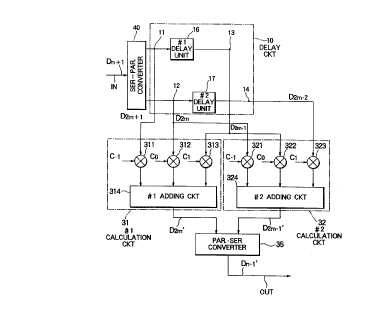
10 Referring to Fig. 3, the description will proceed
to a transversal filter of a parallel processing type
according to a first embodiment of this invention. The
transversal filter is similar in structure and operation
to the conventional transversal filter illustrated in
15 Fig. 1 except that the transversal filter comprises a
serial-parallel converter 40 in place of the first and
the second latch circuits 21 and 22. In addition, the
delay circuit is modified in the manner which will later
be described. The delay circuit is therefore depicted at
20 the reference numeral 10. In the transversal filter, the
input signal IN and the output signal OUT have the input
and the output data rates which are equal to each other.
The serial-parallel converter 40 is supplied with
the input signal IN or Dn+1' The serial-parallel
converter 40 converts the input signal IN into first and
M-th parallel converted signals, where M represents a
second positive integer which is not less than two. In
the example being illustrated, the second positive
21
integer M is equal to two and the serial-parallel
converter 40 therefore produces the first and the second
parallel converted signals D2m+1 and D2m'
The first and the second parallel converted
signals D2m+1 and D2m are supplied to the delay circuit
10. The delay circuit 10 has first through L-th taps,
where L represents a third positive integer which is
larger than the first positive integer J. In the example
being illustrated, the third positive integer L is equal
to four and the delay circuit 10 therefore has the first
through the fourth taps 11, 12, 13, and 14. The first
parallel converted signal D2m+1 is supplied to the first
tap 11 while the second parallel converted signal D2m is
supplied to the second tap 12. The first tap 11 produces
the first parallel converted signal D2m+1 as a first tap
signal as it is. Likewise, the second tap 12 produces
the second parallel converted signal D2m as a second tap
signal as it is. The delay circuit 10 comprises first
and second delay units 16 and 17 which are placed between
the first and the third taps 11 and 13 and between the
second and the fourth taps 12 and 14, respectively. Each
of the first and the second delay units 16 and 17
provides twice the unit delay which is substantially
equal to the reciprocal of the input data rate.
The first parallel converted signal D2m+1 is
delivered to the first tap 11 and successively delayed by
the first delay unit 16 to be produced as a third tap
22
signal D2m-1 which is sent to the third tap 13.
Likewise, the second parallel converted signal D2m is
delivered to the second tap 12 and successively delayed
by the second delay unit 17 to be produced as a fourth
tap signal D2m-2 which is sent to the fourth tap 14. At
any rate, the delay circuit 10 produces the first through
the fourth tap signals D , D , D , and D
2m+1 2m 2m-1 2m-2'
The first through the third tap signals D2m+1'
D2m, and D2m-1 are supplied to the first calculation
circuit 31 as first through third primary tap signals,
respectively. The second through the fourth tap signals
D2m' D2m-1' and D2m-2 are supplied to the second
calculation circuit 31 as first through third subsidiary
tap signals, respectively.
In the first calculation circuit 31, the first
through the third primary multiplying circuits 311 to 313
are supplied with the first through the third primary tap
signals D2m+1' D2m' and D2m-1. The first primary
multiplying circuit 311 multiplies the first primary tap
signal D2m+1 by the first tap gain C-1 to produce a first
primary product signal indicative of a product of the
first primary tap signal D2m+1 and the first tap gain
C-1. The second primary multiplying circuit 312
multiplies the second primary tap signal D2m by the
second tap gain CO to produce a second primary product
signal indicative of a product of the second primary tap
signal D2m and the second tap gain C0. The third primary
multiplying circuit 313 multiplies the third primary tap
23 2~.I36~~
signal D2m-1 by the third tap gain Cl to produce a third
primary product signal indicative of a product of the
third primary tap signal D2m-1 and the third tap gain C1.
The first through the third primary product signals are
supplied to the first adding circuit 314. The first
adding circuit 314 adds up three terms of the first
through the third primary product signals to produce a
first addition result signal D2m' indicative of a first
addition result of the three terms.
In the second calculation circuit 32, the first
through the third subsidiary multiplying circuits 321 to
323 are supplied with the first through the third
subsidiary tap signals D2m. D2m-1' and D2m-2. The first
subsidiary multiplying circuit 321 multiplies the first
subsidiary tap signal D2m by the first tap gain C-1 to
produce a first subsidiary product signal indicative of a
product of the first subsidiary tap signal D2m and the
first tap gain C-1. The second subsidiary multiplying
circuit 322 multiplies the second subsidiary tap signal
D2m-1 by the second tap gain CO to produce a second
subsidiary product signal indicative of a product of the
second subsidiary tap signal D2m-1 and the second tap
gain C0. The third subsidiary multiplying circuit 323
multiplies the third subsidiary tap signal D2m-2 by the
third tap gain Cl to produce a third subsidiary product
signal indicative of a product of the third subsidiary
tap signal D2m-2 and the third tap gain C1. The first
through the third subsidiary product signals are supplied
24
to the second adding circuit 324. The second adding
circuit 324 adds up three terms of the first through the
third subsidiary product signals to produce a second
addition result signal D2m-1' indicative of a second
5addition result of the three terms.
The first and the second addition result signals
D2m' and D2m-1' are supplied to the parallel-serial
converter 35. The parallel-serial converter 35 carries
out a parallel-serial conversion on or couples the first
l0and the second addition result signals D2m' and D2m-1' to
produce a serial converted signal Dn-1' as the output
signal OUT.
As apparent from the above description, the first
and the second addition result signals D2m' and D2m-1~
l5are given by:
D2m' - C-1 x D2m+1 + CO x D2m + Cl x D2m-l,
and D2m-1' C-1 x D2m + CO x D2m-1 + Cl x D2m-2'
The output signal OUT or the serial converted
signal Dn' is therefore given by:
20 Dn' - C-1 x Dn+1 + CO x Dn + C1 x Dn-1'
Referring to Fig. 4 in addition to Fig. 3,
description will be directed to operation of the
transversal filter illustrated in Fig. 3. First through
ninth input time slots are indicated along a first or top
25 line in Fig. 4 by numerals 1 through 9.
The input signal IN or Dn+1 is indicated along a
second line. Third through sixth lines show the first
25
through the fourth tap signals D2m+1' D2m' D2m-1' and
D2m-2' respectively. Seventh through ninth lines show
the first through the third primary tap signals D2m+1'
D2m, and D2m-1 which are supplied to the first through
5the third primary multiplying circuits 311 to 313 in the
first calculation circuit 31, respectively. Tenth
through twelfth lines show the first through the third
subsidiary tap signals D2m. D2m-1' and D2m-2 which are
supplied to the first through the third subsidiary
lOmultiplying circuits 321 to 323 in the second calculation
circuit 32, respectively. Thirteenth and fourteenth
lines show the first and the second addition result
signals D2m' and D2m-1', respectively. A fifteenth line
shows the output signal OUT or the serial converted
l5signal Dn-1~.
The input signal IN or Dn+1 comprises a series of
input elements such as first through ninth input elements
Dl, D2, D3, D4, D5, D6, D~, D8, D9 of the first through
the ninth input time slots 1 to 9.
20 The first tap signal D2m+1 comprises a series of
primary tap elements having input time slots each of
which is equal in number to an odd number such as the
first input element D1 of the first input time slot 1,
the third input element D3 of the third input time slot
25 3. the fifth input element D5 of the fifth input time
slot 5, the seventh input element D~ of the seventh input
time slot 7. The second tap signal D2m comprises a
series of secondary tap elements having input time slots
26
each of which is equal in number to an even number such
as a zeroth input element DO of a zeroth input time slot
0, the second input element D2 of the second input time
slot 2, the fourth input element D4 of the fourth input
time slot 4, the sixth input element D6 of the sixth
input time slot 6. The third tap signal D2m-1 comprises
a series of tertiary tap elements having input time slots
each of which is equal in number to an odd number such as
one time slot previous to the zeroth or a (-1)-th input
element D-1 of a (-1)-th input time slot -1, the first
input element Dl of the first input time slot 1, the
third input element D3 of the third input time slot 3,
the fifth input element D5 of the fifth input time slot
5. The fourth tap signal D2m-1 comprises a series of
quaternary tap elements having input time slots each of
which is equal to an even number such as two time slots
previous to the zeroth or a (-2)-th input element D-2 of
a (-2)-th input time slot -2, the zeroth input element DO
of the zeroth input time slot 0, the second input element
D2 of the second input time slot 2, the fourth input
element D4 of the fourth input time slot 4.
The first through the third primary tap signals
D2m+1' D2m' and D2m-1 are equal to the first through the
fourth tap signals D2m+1' D2m' and D2m-1' respectively.
The first through the third subsidiary tap signals D2m'
D2m-1' and D2m-2 are equal to the second through the
fourth tap signals D , D , and D
2m 2m-1 2m-2' respectively.
~~13fi~~
27
The first addition result signal D2m' comprises a
series of addition result elements having output time
slots each of which is equal in number to an even number
such as a zeroth addition result element DO' of a zeroth
output time slot, a second addition result element D2' of
a second output time slot, a fourth addition result
element D4' of a fourth output time slot, a sixth
addition result element D6' of a sixth output time slot.
Similarly, the second addition result signal D2m-1~
comprises a series of addition result elements having
output time slots each of which is equal in number to an
odd number such as a (-1)-th addition result element D-1'
of a (-1)-th output time slot, a first addition result
element Dl' of a first output time slot, a third addition
result element D3' of a third output time slot, a fifth
addition result element D5' of a fifth output time slot.
The output signal OUT or the serial converted
signal Dn-1' comprises a series of the addition result
elements such as the (-1)-th through the sixth addition
result elements D-1' to D6' of the (-1)-th through the
sixth output time slots.
Referring to Fig. 5, the description will proceed
to a transversal filter of a parallel processing type
according to a second embodiment of this invention. The
transversal filter is similar in structure and operation
to the conventional transversal filter illustrated in
Fig. 1 except that the transversal filter comprises the
serial-parallel converter 40 and the delay circuit is
~~~.3~a6
modified in the manner which will later be described.
The delay circuit is therefore depicted at the reference
numeral 10a. In the transversal filter, the input signal
IN has the input data rate which is twice the output data
rate of the output signal OUT. The illustrated
transversal filter is a transversal filter having a tap
interval which is a half of a symbol interval and the
illustrated transversal filter is applicable to the
digital filter such as the interference canceller or the
roll-off filter. In the example being illustrated, the
input signal IN is a digital signal having waveform
shaped. Such a digital signal is a baseband digital
signal which is obtained by demodulating and decision a
digital modulated signal. Its decision timing has an
interval which is a half of the symbol interval. In
other words, the input data rate is twice a bit rate of
the input signal IN.
The serial-parallel converter 40 is supplied with
the input signal IN or D~.5(k+1)' The serial-parallel
converter 40 converts the input signal IN into first and
second parallel converted signals Dn+0.5 and Dn.
The first and the second parallel signals Dn+0.5
and Dn are supplied to the delay circuit 10a. The delay
circuit 10 has first through L-th taps, where L
represents the third positive integer which is larger
than the first positive integer J. In the example being
illustrated, the third positive integer is equal to five
and the delay circuit l0a therefore has the first through
2113~~b
29
the fifth taps 11, 12, 13, 14, and 15. The first
parallel converted signal Dn+0.5 is supplied to the first
tap 11 while the second parallel converted signal Dn is
supplied to the second tap 12. The first tap 11 produces
the first parallel converted signal D as a first tap
n+0.5
signal as it is. Likewise, the second tap 12 produces
the second parallel converted signal Dn as a second tap
signal as it is. The delay circuit l0a comprises first
through third delay units 16a, 17a, and 18a which are
placed between the first and the third taps 11 and 13,
between the second and the fourth taps 12 and 14, and
between the third and the fifth taps 13 and 15,
respectively. Each of the first through the third delay
units 16a, 17a, and 18a provides twice the unit delay
which is substantially equal to the reciprocal of the
input data rate.
The first parallel converted signal Dn+0.5 is
delivered to the first tap 11 and successively delayed by
the first delay unit 16a to be produced as a third tap
signal D which is sent to the third tap 13.
n-0.5
Likewise, the second parallel converted signal Dn is
delivered to the second tap 12 and successively delayed
by the second delay unit 17a to be produced as a fourth
tap signal Dn_1.0 which is sent to the fourth tap 14.
The third tap signal Dn_0.5 is delayed by the third delay
unit 18a to be produced as a fifth tap signal Dn_1.5
which is sent to the fifth tap 15. At any rate, the
delay circuit l0a produces the first through the fifth
~~~3fia~
tap signals Dn+0.5' Dn' Dn-0.5' Dn-1.0' and Dn-1.5'
The first through the third tap signals Dn+0.5'
Dn, and Dn-0.5 are supplied to the first latch circuit
21. The first latch circuit 21 latches the first through
5 the third tap signals Dn+0.5' Dn' and Dn-0.5 and holds
these signals during a time duration corresponding to
four input time slots of the input signal IN to produce
first through third primary latched signals D2m+0.5' D2m'
and D2m-0.5' Likewise, the third through the fifth tap
10 signals Dn_0.5' Dn-l.p' and Dn-1.5 are supplied to the
second latch circuit 22. The second latch circuit 22
latches the third through the fifth tap signals Dn_0.5'
Dn-1.0' and Dn-1.5 and holds these signals during the
time duration corresponding to the four time slots to
15 produce first through third subsidiary latched signals
D2m-0.5' D2m-1.0' and D2m-1.5'
The first through the third primary latched
signals D2m+0.5' D2m' and D2m-0.5 are supplied to the
first calculation circuit 31 as first through third
20 primary tap signals, respectively. The first through the
third subsidiary latched signals D2m-0.5' D2m-1.0~ and
D2m-1.5 are supplied to the second calculation circuit 31
as first through third subsidiary tap signals,
respectively.
25 In the first calculation circuit 31, the first
through the third primary multiplying circuits 311 to 313
are supplied with the first through the third primary tap
2~i3666
31
signals D2m+0.5' D2m' and D2m-0.5' The first primary
multiplying circuit 311 multiplies the first primary tap
signal D2m+0.5 by the first tap gain C-1 to produce a
first primary product signal indicative of a product of
5the first primary tap signal D2m+0.5 and the first tap
gain C-1. The second primary multiplying circuit 312
multiplies the second primary tap signal D2m by the
second tap gain CO to produce a second primary product
signal indicative of a product of the second primary
tap signal D2m and the second tap gain C0. The third
primary multiplying circuit 313 multiplies the third
primary tap signal D2m-0.5 by the third tap gain C1 to
produce a third primary product signal indicative of a
product of the third primary tap signal D2m-0.5 and
l5the third tap gain Cl. The first through the third
primary product signals are supplied to the first adding
circuit 314. The first adding circuit 314 adds up
three terms of the first through the third primary
product signals to produce a first addition result signal
D2m~ indicative of a first addition result of the three
terms.
In the second calculation circuit 32, the first
through the third subsidiary multiplying circuits 321 to
323 are supplied with the first through the third
subsidiary tap signals D
2m-0.5' D2m-1.0' and D2m-1.5'
The first subsidiary multiplying circuit 321 multiplies
the first subsidiary tap signal D2m-0.5 by the first tap
~~~~6
32
gain C-1 to produce a first subsidiary product signal
indicative of a product of the first subsidiary tap
signal D2m-0.5 and the first tap gain C-1. The second
subsidiary multiplying circuit 322 multiplies the second
5subsidiary tap signal D2m-1.0 by the second tap gain CO
to produce a second subsidiary product signal indicative
of a product of the second subsidiary tap signal D2m-1.0
and the second tap gain C0. The third subsidiary
multiplying circuit 323 multiplies the third subsidiary
lOtap signal D2m-1.5 by the third tap gain Cl to produce a
third subsidiary product signal indicative of a product
of the third subsidiary tap signal D2m-1.5 and the third
tap gain C1. The first through the third subsidiary
product signals are supplied to the second adding circuit
15324. The second adding circuit 324 adds up three terms
of the first through the third subsidiary product signals
to produce a second addition result signal D2m-1' indica-
tive of a second addition result of the three terms.
The first and the second addition result signals
20D2m~ and D2m-l~ are supplied to the parallel-serial
converter 35. The parallel-serial converter 35 carries
out a parallel-serial conversion on or couples the first
and the second addition result signals D2m' and D2m-1' to
produce a serial converted signal Dn-1' as the output
25signal OUT.
As apparent from the above description, the first
and the second addition result signals D2m' and D2m-1~
are given by:
33
D2m' - C-1 x D2m+0.5 + Cp x D2m + Cl x D2m_0.5'
and D2m-1~ C-1 x D2m-0.5 + CO x D2m-1.0 + C1 x D2m-1.5'
The output signal OUT or the serial converted
signal Dn' is therefore given by:
Dn' - C-1 x Dn+0.5 + Cp x Dn + C1 x Dn_p.5'
Referring to Fig. 6 in addition to Fig. 5,
description will be directed to operation of the
transversal filter illustrated in Fig. 5. First through
eighteenth input time slots are indicated along a first
or top line in Fig. 6 by numerals 1 through 18.
The input signal IN or Dp.S(k+1) is indicated
along a second line. Third through seventh lines show
the first through the fifth tap signals Dn+0.5' Dn'
Dn-0.5' Dn-1.0' and Dn_1.5' respectively. Eighth through
tenth lines show the first through the third primary tap
signals D2m+0.5' D2m' and D2m-0.5 which are supplied to
the first through the third primary multiplying circuits
311 to 313 in the first calculation circuit 31,
respectively. Eleventh through thirteenth lines show the
first through the third subsidiary tap signals D2m-0.5'
D2m-1.0' and D2m-1.5 which are supplied to the first
through the third subsidiary multiplying circuits 321 to
323 in the second calculation circuit 32, respectively.
Fourteenth and fifteenth lines show the first and the
second addition result signals D2m' and D2m-1~'
respectively. A sixteenth line shows the output signal
OUT or the serial converted signal Dn-1'.
~1~35~~
34
The input signal IN or D0.5(k+1) comprises a
series of input elements such as first through eighteenth
input elements D0.5. D1.0' D1.5' D2.0' D2.5' D3.0' D3.5'
D4.0' D4.5' D5.0' D5.5' D6.0' D6.5' D7.0' D7.5' D8.0'
D8.5, and D9.0 of the first through the eighteenth input
time slots 1 to 18.
The first tap signal Dn+0.5 comprises a series of
primary tap elements having input time slots each of
which is equal in number to an odd number such as the
first input element D0.5 of the first input time slot 1,
the third input element D1.5 of the third input time slot
3, the fifth input element D2_5 of the fifth input time
slot 5, the seventh input element D3.5 of the seventh
input time slot 7, the ninth input element D4.5 of the
ninth input time slot 9, the eleventh input element D5.5
of the eleventh input time slot 11, the thirteenth input
element D6.5 of the thirteenth input time slot 13, the
fifteenth input element D~.S of the fifteenth input time
slot 15, the seventeenth input element D8.5 of the
seventeenth input time slot 17.
The second tap signal Dn comprises a series of
secondary tap elements having input time slots each of
which is equal in number to an even number such as a
zeroth input element D0.0 of a zeroth input time slot 0,
the second input element D1.0 of the second input time
slot 2, the fourth input element D2.0 of the fourth input
time slot 4, the sixth input element D3.0 of the sixth
2~~3~fl
input time slot 6, the eighth input element D4.0 of the
eighth input time slot 8, the tenth input element D5.0 of
the tenth input time slot 10, the twelfth input element
D6.0 of the twelfth input time slot 12, the fourteenth
5input element D~.O of the fourteenth input time slot 14,
the sixteenth input element D8.0 of the sixteenth input
time slot 16.
The third tap signal Dn-0,5 comprises a series of
tertiary tap elements having input time slots each of
lOwhich is equal in number to an odd number such as a
(-1)-th input element D-0_5 of a (-1)-th input time slot
-1, the first input element D0.5 of the first input time
slot 1, the third input element D1.5 of the third input
time slot 3, the fifth input element D2.5 of the fifth
l5input time slot 5, the seventh input element D3,5 of the
seventh input time slot 7, the ninth input element D4.5
of the ninth input time slot 9, the eleventh input
element D5.5 of the eleventh input time slot 11, the
thirteenth input element D6.5 of the thirteenth input
20time slot 13, the fifteenth input element D~.S of the
fifteenth input time slot 15.
The fourth tap signal Dn-1.0 comprises a series
of quaternary tap elements having input time slots each
of which is equal to an even number such as a (-2)-th
25input element D-1.0 of a (-2)-th input time slot -2, the
zeroth input element D0.0 of a zeroth input time slot 0,
the second input element D1.0 of the second input time
36 2~~36a
slot 2, the fourth input element D2_0 of the fourth input
time slot 4, the sixth input element D3.0 of the sixth
input time slot 6, the eighth input element D4.0 of the
eighth input time slot 8, the tenth input element D5.0 of
5the tenth input time slot 10, the twelfth input element
D6.0 of the twelfth input time slot 12, the fourteenth
input element D~.O of the fourteenth input time slot 14.
The fifth tap signal Dn-1.5 comprises a series of
quinary tap elements having input time slots each of
lOwhich is equal to an odd number such as a (-3)-th input
element D-1.5 of a (-3)-th input time slot -3, the
(-1)-th input element D-0.5 of a (-1)-th input time slot
-1, the first input element D0.5 of the first input time
slot 1, the third input element D1.5 of the third input
l5time slot 3, the fifth input element D2.5 of the fifth
input time slot 5, the seventh input element D3.5 of the
seventh input time slot 7, the ninth input element D4.5
of the ninth input time slot 9, the eleventh input
element D5.5 of the eleventh input time slot 11, the
20thirteenth input element D6.5 of the thirteenth input
time slot 13.
The first primary tap signal D2m+0.5 comprises a
series of primary latched elements having (4n+1)-th input
time slots such as the first input element D0,5 of the
25first input time slot 1, the fifth input element D2.5 of
the fifth input time slot 5, the ninth input element D4.5
of the ninth input time slot 9, the thirteenth input
21~3~Q~
element D6.5 of the thirteenth input time slot 13. The
second primary tap signal D2m comprises a series of
primary latched elements having (4n)-th input time slots
such as the zeroth input element D0.0 of a zeroth input
time slot 0, the fourth input element D2.0 of the fourth
input time slot 4, the eighth input element D4,0 of the
eighth input time slot 8, the twelfth input element D6.0
of the twelfth input time slot 12. The third primary tap
signal D2m-0.5 comprises a series of primary latched
elements having (4n-1)-th input time slots such as the
(-1)-th input element D-0.5 of the (-1)-th input time
slot -1, the third input element D1,5 of the third input
time slot 3, the seventh input element D3.5 of the
seventh input time slot 7, the eleventh input element
D5.5 ~f the eighth input time slot 11.
The first subsidiary tap signal D2m-0.5 comprises
a series of subsidiary latched elements having (4n-1)-th
input time slots such as the (-1)-th input element D-0.5 of
the (-1)-th input time slot -1, the third input element
D1.5 of the third input time slot 3, the seventh input
element D3.5 of the seventh input time slot 7, the eleventh
input element D5.5 of the eleventh input time slot 11.
The second subsidiary tap signal D2m-1.0 Comprises a
series of subsidiary latched elements having (4n-2)-th
input time slots such as the (-2)-th input element D-1.0
of the (-2)-th input time slot -2, the second input
element D1.0 of the second input time slot 2, the sixth
input element D3.0 of the sixth input time slot 6, the
38
tenth input element D5.0 of the tenth input time slot 10.
The third subsidiary tap signal D2m-1.5 comprises a
series of subsidiary latched elements having (4n-3)-th
input time slots such as the (-3)-th input element D-1.5
of the (-3)-th input time slot -3, the first input
element D0.5 of the first input time slot 1, the fifth
input element D2.5 of the fifth input time slot 5, the
ninth input element D4.5 of the ninth input time slot 9.
The first addition result signal D2m' comprises a
series of addition result elements having output time
slots each of which is equal in number to an even number
such as a zeroth addition result element D0.0' of a
zeroth output time slot, a second addition result element
D2.0' of a second output time slot, a fourth addition
result element D4.0' of the fourth output time slot, a
sixth addition result element D6.0' of the sixth output
time slot. Similarly, the second addition result signal
D2m+1~ comprises a series of addition result elements
having output time slots each of which is equal in number
to an odd number such as a (-1)-th addition result
element D-1.0' of a (-1)-th output time slot, a first
addition result element D1.0' of a first output time
slot, a third addition result element D3.0' of a third
output time slot, a fifth addition result element D5.0'
of a fifth output time slot.
The output signal OUT or the serial converted
signal Dn-1' comprises a series of the addition result
elements such as the (-1)-th through the sixth addition
39
result elements D_1.0' to D6.0' of the (-1)-th through
the sixth output time slots.
In the above-mentioned embodiments, the
serial-parallel converter 40 carries out serial-parallel
5conversion on the digital input signal IN into which an
analog input signal is converted by an analog-to-digital
converter (not shown).
Referring to Fig. 7, the description will be
directed to another serial-parallel converter 40a. The
serial-parallel converter 40a is supplied with the analog
input signal depicted at INa instead of the digital input
signal IN. In addition, the serial-parallel converter
40a is supplied with an input clock signal CLK having a
clock frequency which is equal to a half of the input
data rate of the analog input signal INa.
The serial-parallel converter 40a comprises first
and second analog-to-digital (A/D) converter 41a and 42a
and an inverting circuit 43a. The first A/D converter
41a is supplied with the analog input signal INa and the
input clock signal CLK. The first A/D converter 41a
converts the analog input signal INa into.a first digital
converted signal D2m in synchronism with the input clock
signal CLK. In particular, the first A/D converter 41a
converts, in response to leading edge of the input clock
signal CLK, input analog values of the analog input
signal INa into the first digital converted signal D2m'
The first digital converted signal D2m is produced as the
second parallel converted signal.
40 21I36~6
The inverting circuit 43a is supplied with the
input clock signal CLK. The inverting circuit 43a
inverts the input clock signal CLK to produce an inverted
clock signal CLK. The inverted clock signal CLK is
supplied to the second A/D converter 42a which is
supplied with the analog input signal INa. The second
A/D converter 42a converts the analog input signal INa
into a second digital converted signal D2m+1 in
synchronism with the inverted clock signal CLK. In
particular, the second A/D converter 42a converts, in
response to leading edge of the inverted clock signal
CLK, input analog values of the analog input signal INa
into the second digital converted signal D2m+1' The
second digital converted signal D2m+1 is produced as the
first parallel converted signal.
At any rate, the analog input signal INa is
converted into the first and the second digital converted
signals D2m and D2m+1 by the first and the second A/D
converters 41a and 42a at two different timings.
Turning to Fig. 8 in addition to Fig. 7,
description will be directed to operation of the
serial-parallel converter 40a. The analog input signal
INa is indicated along a first or top line in Fig. 8.
Second and third lines show the input clock signal CLK
and the inverted clock signal CLK, respectively. Fourth
and fifth lines show the first and the second digital
converted signals D2m and D2m+1' respectively.
41 2~~.3s~~
The analog input signal INa comprises a series of
zeroth through seventh input analog values DaO, Dal, Da2,
Da3, Da4, DaS, Da6, and Dad. The input clock signal CLK
has the leading edges where the input analog values each
of which is equal in number to an even number such as the
zeroth input analog value DaO, the second input analog
value Da2, the fourth input analog value Da4, the sixth
input analog value Da6 are present. The inverted clock
signal CLK has the leading edges where the input analog
values each of which is equal in number to an odd number
such as the first input analog value Dal, the third input
analog value Da3, the fifth input analog value DaS, the
seventh input analog value Dad are present.
It will be assumed that the zeroth through the
seventh input analog values Da0 to Dad correspond to
zeroth through seventh digital values D0, Dl, D2, D3, D4,
D5, D6, and D~, respectively. The first digital converted
signal D2m comprises a series of primary digital converted
elements having the digital values each of which is equal
in number to an even number such as the zeroth digital
value D0, the second digital value D2, the fourth digital
value D4, the sixth digital value D6. The second digital
converted signal D2m+1 comprises a series of secondary
digital converted elements having the digital values each
of which is equal in number to an odd number such as the
first digital value Dl, the third digital value D3, the
fifth digital value D5, and the seventh digital value
42
2~.I3fi
While this invention has thus far been described
in conjunction with a few embodiments thereof, it will
now be readily possible for those skilled in the art to
put this invention into practice in various other
manners.