Note: Descriptions are shown in the official language in which they were submitted.
CA 02113836 2001-O1-16
72465-58
1
DESCRIPTION
METHOD AND APPARATUS FOR IDENTIFYING OBJECTS USING COMPOUND
SIGNAL AND A DETECTOR. EMPLOYING AN ELECTRICAL STATIC COUPLING
TECHNIQUE
Technical Field
The present :invention relates to a method, its
electroscope, and an input circuit of the electroscope for
identifying electrically conductive objects to be identified,
e.g., for identifying at least one cable among a plurality of
cables contained in a housing (hereinafter referred to as
"trough") such as a trough for railroads and a terminal box.
Background Art
A trough usually contains a few dozen cables. These
cables may include ones, the service lives thereof having
expired due to deterioration with time or ones that have
incurred failures and are not serviceable. In such a
situation, when a new cable or cables are to be laid in the
trough, it frequently happens that the new cable cannot be laid
unless such unusable cables are removed from the trough.
when laying ~~ new cable, however, a worker may not be
able to identify which cable or cables in the trough are
necessary and which one: or ones are unnecessary. For this
reason, there is a marked increase in the number of cases where
workers are unable to remove unnecessary cables from troughs.
In addition, accidents wherein workers erroneously remove
cables in service when laying new cables have occurred.
Therefore, in this technical field, there has been a demand for
an apparatus which enables workers to open the cover of a
trough in a desired place and locate a particular cable.
CA 02113836 2001-O1-16
72465-58
2
In the past, in response to such a demand, there was
a method whereby a cab:Le was identified by applying a 100VAC
voltage to a conductor of the cable to be removed and detecting
the voltage by using a commercially available electroscope.
However, a 100VAC voltage is constantly applied to most cables
in troughs. In this method, therefore, a plurality of cables
occasionally react at t:he same time, making it difficult to
identify cables. Furthermore, there is such a danger that a
worker may get an electric shock from touching a cable to which
the 100VAC voltage is applied.
So, as anothet~ identifying method, there was a method
wherein a prescribed current is let flow through a particular
cable to be removed, the cable in the trough is clamped with a
cable probe consisting of a search coil, and the current
flowing through the cable is detected using an electromagnetic
induction method, thereby identifying the particular cable.
This identifying method, however, presented a problem
in that a circuit such as a common grounded circuit for letting
currents flow through a. cable to be removed was required. The
identifying method had another problem in that its cable
identifying reliability was low because it was susceptible to
noises in its surroundings. There was still another problem in
that if the identifying' method was used for a portable
apparatus, dry cells for causing currents to flow through
cables were exhausted quickly.
Moreover, according to the identifying method, cables
must be clamped and checked one by one using the search coil to
locate a particular cable among a plurality of cables by
increasing sensitivity, thus resulting in poor work efficiency.
3~
CA 02113836 2001-O1-16
72465-58
3
Disc:Losure of the Invention
An object of the present invention is to provide a
method for identifying objects to be identified, which method
enables improved work efficiency of identifying electrically
conductive objects to be identified.
Another object of the present invention is to provide
a method for identifying objects to be identified, which method
enables higher immunity to noises in surroundings and higher
reliability in identifying objects to be identified.
1~ Still another object of the present invention is to
provide a method for identifying objects to be identified,
which method makes it possible to reduce the exhaustion of dry
cells.
Yet another object of the present invention is to
provide a method for identifying objects to be identified,
wherein a judgement standard for identifying objects to be
identified is automatically set in accordance with the
conditions of the objects to be identified.
To fulfill the objects described above, the method
2() for identifying objects to be identified according to the
present invention is provided with an applying step for
directly applying a sig:aal of a specific frequency from an
oscillating circuit to a particular object to be identified
among a plurality of electrically conductive objects to be
identified which are stored in a particular housing, and an
identifying step wherein the signal of the aforesaid specific
frequency is detected among the aforesaid particular object to
be identified through a detecting section which employs an
electrostatic coupling method, thereby identifying the
3U aforesaid particular object to be identified.
CA 02113836 2001-O1-16
72465-58
4
The signal oi= the specific frequency applied by the
applying section to the' particular object to be identified is
comprised of a compound signal of a plurality of frequency
signals having different frequencies; the compound signal is
detected through an electrostatic coupling type non-contact
detecting section, and the detected signal is subjected to gain
adjustment.
As described above, according to the present
invention, the compound signals applied by the applying section
1~~ are detected by the detecting section from the individual
objects to be identified., thus identifying particular objects
to be identified which are not in service. Specifically, when
the identifying method according to the present invention is
used for identifying cables, there is almost zero probability
that a potential signal having the same level as that of the
compound signal exists at the same time in a cable which is
actually being used; therefore, the particular cables can be
identified efficiently ~~ithout making erroneous judgement.
In summary, this invention seeks to provide a method
for identifying a specified object from among a plurality of
electrically conductive objects contained in a housing, the
method comprising the steps of: an applying step of:
compounding a plurality «f signals with predetermined different
frequencies, generated f-_rom a plurality of oscillating
circuits, at substantially uniform signal levels by means of a
compounding/applying circuit to obtain a compound signal, and
directly applying the compound signal to the specified object;
and a detecting step of.: detecting a potential signal from one
of the objects by means of a detecting section which employs an
electrostatic coupling method; separating a plurality of
signals with the predetermined different frequencies from the
potential signal by means of band-pass filters having passbands
thereof corresponding to the predetermined different
CA 02113836 2001-O1-16
72465-58
frequencies, respectively; determining magnitudes and
uniformity of signal levels of the separated signals by means
of comparator circuits; and judging that said one object is the
specified object only when the detected potential signal is
5 found to be identical with the compound signal directly applied
to the specified object.
The invent10I1 further provides a method for
identifying a specified object from among a plurality
electrically conductive objects contained in a housing, the
method comprising the steps of: an applying step of;
compounding a plurality of signals with predetermined different
frequencies, generated from a plurality of oscillating
circuits, at signal levels having a prescribed proportional
relationship by means of a compounding/applying circuit to
obtain a compound signal, and directly applying the compound
signal to the specified object; and a detecting step of:
detecting a potential ~>ignal from one of the objects by means
of a detecting section which employs an electrostatic coupling
method; separating a plurality of signals with the
predetermined different. frequencies from the potential signal
by means of band-pass filters having passbands thereof
corresponding to the predetermined different frequencies,
respectively; determining magnitudes and proportional
relationship of signal levels of the separated signals by means
of comparator circuits; and judging that said one object is the
specified object only when the detected potential signal is
found to be identical with the compound signal directly applied
to the specified object.
The invention. further provides a method for
identifying a specified. object from among a plurality of
electrically conductive objects contained in a housing, the
method comprising; an applying step of: compounding signals of
a plurality of signals with predetermined different
CA 02113836 2001-O1-16
72465-58
6
frequencies, generated from a plurality of oscillating
circuits, at substantially uniform signal levels in different
combinations of frequencies by means of a combining/compounding
circuit to obtain a plurality of compound signals; and directly
!~ applying each of said compound signals to the corresponding
ones of specified objects; and a detecting step of: detecting a
potential signal from one of the objects by means of a
detecting section which employs an electrostatic coupling
method; separating a plurality of signals with the
1c) predetermined differernt frequencies from the potential signal
by means of band-pass filters having passbands thereof
corresponding to the predetermined different frequencies,
respectively; determining the frea_uency combination of the
separated signals by means of a combining circuit; determining
15 magnitudes and uniformity of signal levels of the determined
signals by means of comparator circuits; and judging that said
one object is the specified object only when the detected
potential signal is found to be identical with the compound
signal directly applied to the specified object.
2U The invention further provides a method for
identifying a specified object from among a plurality of
electrically conductive objects contained in a housing, the
method comprising the seeps of: an applying step of:
compounding a plurality of signals with predetermined different
25 frequencies, generated from a plurality of oscillating
circuits, at signal levels having a prescribed proportional
relationship and in dif:~erent combinations of frequencies by
means of a combining/compounding circuit to obtain a plurality
of compound signals; and directly applying the compound signals
3U to corresponding ones o:E specified objects; and a detecting
step of: detecting a potential signal from one of the objects
by means of a detecting section which employs an electrostatic
coupling method; separating a plurality of signals with the
CA 02113836 2001-O1-16
72465-58
7
predetermined different: frequencies from the potential signal
by means of band-pass f=filters having passbands thereof
corresponding to the px.-edetermined different frequencies,
respectively; determining the frequency combination of the
separated signals by mE:ans of a combining circuit; determining
magnitudes and proportional relationship of signal levels of
the determined signals by means of comparator circuits; and
judging that said one object is the specified object only when
the detected potential signal is found to be identical with the
compound signal directly applied to the specified object.
The invention further provides an apparatus for
identifying a specified object from among a plurality of
electrically conductive objects contained in a housing, the
apparatus comprising: oscillating circuits for generating a
plurality of signals having predetermined different
frequencies, respectively; a compounding/applying circuit for
compounding said plurality of generated signals at
substantially uniform ~~ignal levels by means of an amplifier to
obtain a compound signal, and for directly applying the
compound signal to the specified object; a detecting section
for detecting a potential signal from one of the objects by an
electrostatic coupling method; and an identifying circuit
including: band-pass filters having passbands thereof
corresponding to the predetermined different frequencies,
respectively, and separating a plurality of signals with the
predetermined different: frequencies from the detected potential
signal only when the potential signal is detected from said one
object; and comparator circuits for identifying the specified
object by determining magnitudes and uniformity of signal
levels of the separated signals.
The invention further provides an apparatus for
identifying a specified object from among a plurality of
electrically conductive objects contained in a housing, the
CA 02113836 2001-O1-16
72465-58
8
apparatus comprising: oscillating circuits for generating a
plurality of signals having predetermined different
frequencies, respectively; a compounding/applying circuit for
compounding said plurality of generated signals at signal
levels having a prescribed proportional relationship by means
of an amplifier to obtain a compound signal, and for directly
applying the compound signal to the specified object; a
detecting section for detecting a potential signal from one of
the objects by an electrostatic coupling method; and an
identifying circuit including: band-pass filters having
passbands thereof corresponding to the predetermined different
frequencies, respectively, and separating a plurality of
signals with the predetermined different frequencies from the
detected potential signal one when the potential signal is
detected from said one object, and comparator circuits for
identifying the specified object by determining magnitudes and
proportional relationships of signal levels of the separated
signals.
The invention further provides an apparatus for
2C) identifying a specified object from among a plurality of
electrically conductive objects contained in a housing, the
apparatus comprising: oscillating circuits for generating a
plurality of signals having predetermined different
frequencies, respectively; a combining/compounding circuit for
compounding said plurality of signals with the respective
different frequencies, generated from said oscillating
circuits, at substantially uniform signal levels in different
combinations of frequen~~ies to obtain a plurality of compound
signals; an applying circuit for directly applying said
3C) plurality of compound signals to corresponding ones of
specified objects; a detecting section for detecting a
potential signal from o:ne of the objects by an electrostatic
coupling method; and an identifying circuit including: band-
CA 02113836 2001-O1-16
72465-58
9
pass filters having passbands thereof corresponding to the
predetermined different. frequencies, respectively, and
separating a plurality of signals with the predetermined
different frequencies from the detected potential signal only
when the potential signal is detected from said one object; a
combining circuit for determining the frequency combination of
the separated signals, and comparator circuits for identifying
the specified object by determining magnitudes and uniformity
of signal levels of the separated signals.
The invention. further provides an apparatus for
identifying a specified object from among a plurality of
electrically conductive objects contained in a housing, the
apparatus comprising: oscillating circuits for generating a
plurality of signals having predetermined different
1'.~ frequencies, respectively; a combining/compounding circuit for
compounding said plurality of signals with the respective
different frequencies, generated from said oscillating
circuits, at signal levels having a prescribed proportional
relationship and in different combinations of frequencies to
2c) obtain a plurality of compound signals; an applying circuit for
directly applying said plurality of compound signals to
corresponding ones of specified objects; a detecting section
for detecting a potential signal from one of the objects by an
electrostatic coupling method; and an identifying circuit
25 including: band-pass filters having passbands thereof
corresponding to the predetermined different frequencies,
respectively, and separating a plurality of signals with the
predetermined different frequencies from the detected potential
signal only when the po~~ential signal is detected from said one
3U object; a combining circuit for determining the frequency
combination of the separated signals, and comparator circuits
for identifying the specified object by determining magnitudes
CA 02113836 2001-O1-16
72465-58
and proportional relationship of signal levels of the
determined signals.
The invention further provides a method for
identifying a specified object from among a plurality of
5 electrically conductivE: objects contained in a housing, the
method comprising: an applying step of generating a compound
signal by compounding a plurality of signals with predetermined
different frequencies obtained from an oscillating circuit
section, while keeping a specified one of electrically
10 conductive objects in an ungrounded state and grounding unused
electrically conductive objects and the oscillating circuit
section and directly applying the compound signal to the
specified object; and a. detecting step of detecting a signal
from each of electrically conductive objects by means of a
detecting section employing an electrostatic coupling method
and having sensitivity adjusting means, while adjusting a
sensitivity of the sensitivity adjusting means in accordance
with a voltage level of the detected signal, and identifying
the specified object when the compound signal is detected from
the object.
The invention further provides a method for
identifying a specified object from among a plurality of
electrically conductive objects contained in a housing, the
method comprising: an applying step of generating a compound
2:~ signal by compounding a plurality of signals obtained from an
oscillating circuit section and having predetermined different
frequencies and a uniform signal level, and directly applying
the compound to a specified one of electrically conductive
objects; and a detecting step of detecting signals with the
3~J predetermined different frequencies forming the compound signal
and noise components thereof, which signals are derived from
each of electrically conductive objects, by means of a
detecting section employing an electrastatic coupling method,
CA 02113836 2001-O1-16
72465-58
11
and identifying the specified object by determining magnitudes
and uniformity of the levels of the signals with the different
frequencies based on noise levels of the detected noise
components.
The invention further provides a method for
identifying a specified object from among a plurality of
electrically conductive=_ objects contained in a housing, the
method comprising: an applying step of generating a compound
signal by compounding <~ plurality of signals which are obtained
from an oscillating circuit section, which have predetermined
different frequencies, and of which signal levels have a
predetermined relationship, and directly applying the compound
signal to a specified one of electrically conductive objects;
and a detecting step oi_ detecting signals with the
predetermined different. frequencies forming the compound
signal and noise components thereof, which signals are derived
from each of electrically conductive objects, by means of a
detecting section employing an electrostatic coupling method,
and identifying the specified object by determining the
predetermined relation~~hip and magnitudes of the levels of the
signals with the different frequencies based on noise levels of
the detected noise components.
The invention further provides a method for
identifying a specified object from among a plurality of
electrically conductive: objects contained in a housing, the
method comprising: an applying step of generating a plurality
of compound signals by compounding a plurality of predetermined
combinations of signalse having different frequencies and having
a uniform signal level, which signals are selected from among a
plurality of signals with different frequencies obtained from
an oscillating circuit section, and directly applying the
compound signals to specified ones of electrically conductive
objects, respectively; and a detecting step of detecting
CA 02113836 2001-O1-16
72465-58
12
signals with the different frequencies forming each compound
signal and noise components thereof, which signals are derived
from each of electrically conductive objects, by means of a
detecting section employing an electrostatic coupling method,
and identifying the specified objects by determining magnitudes
and uniformity of the levels of the signals with the different
frequencies based on noise levels of the detected noise
components.
The invention further provides a method for
identifying a specified object from among a plurality of
electrically conductive objects contained in a housing, the
method comprising: an applying step of generating a plurality
of compound signals by compounding a plurality of predetermined
combinations of signals having different frequencies and having
1~~ a predetermined signal :Level relationship, which signals are
selected from among a plurality of signals with different
frequencies obtained from an oscillating circuit section and
directly applying the compound signals to specified ones of
electrically conductive objects, respectively; and a detecting
step of detecting signa7_;s with the different frequencies
forming each compound signal and noise components thereof,
which signals are derive=d from each of electrically conductive
objects, by means of a detecting section employing an
electrostatic coupling method, and identifying the specified
objects by determining t:he predetermined relationship and
magnitudes of the level=~ of the signals with the different
frequencies based on noise levels of the detected noise
components.
Brief Description of Drawings
The drawings ;how an embodiment of the present
invention, wherein FIG. 1 is a block diagram indicating a
configuration of an identifying apparatus which employs the
CA 02113836 2001-O1-16
72465-58
13
first embodiment of the method for identifying an object to be
identified according tc~ the present invention. FIG. 2 is a
waveform chart of a compound signal which is applied to a
conductor of a cable shown in FIG. 1. FIG. 3 is another
S waveform chart of an input signal detected from the conductor
of the cable. FIG. 4 is a principle diagram which shows a
principle of an electroscope according to the present
invention. FIG. 5 is a diagram which shows an equivalent
circuit of the electroscope shown in FIG. 4. FIG. 6 is a
diagram which shows an embodiment of the electroscope shown in
FIG. 4. FIG. 7 is a sectional view taken on line 7-7 in FIG.
6. FIG. 8 is a diagram which shows another embodiment of the
electroscope. FIG. 9 is still another embodiment of the
electroscope. FIG. 10 is yet another embodiment of the
electroscope. FIG. 11 is a sectional view taken on line 11-11
in FIG. 10. FIG. 12 is a still further embodiment of the
electroscope. FIG. 13 is a sectional view taken on line 13-13
in FIG. 12. FIG. 14 is a block diagram which shows the
configuration of an iden~ifying apparatus which employs the
second embodiment of the=_ method for identifying objects to be
identified according to the present invention. FIG. 15 is a
block diagram which shows the configuration of an applying
section shown in FIG. 14. FIG. 16 shows an equivalent circuit
between cables A and B which is set as an example to explain
the influences exerted by an electrostatic coupling capacitance
between the cables. Fic~. 17 and Fig. 18 are principle diagrams
of a typical situation used to explain the principle of the
third embodiment of the method for identifying objects to be
identified according to the present invention and its
equivalent circuit. FIG. 19 and FIG. 20 are also principle
diagrams of another typical situation used to explain the
principle of the third embodiment and its equivalent circuit.
FIG. 21 and FIG. 22 are also a principle diagram of still
another typical situatic>n used to explain the principle of the
CA 02113836 2001-06-12
72465-58
14
third embodiment and its equivalent circuit. FIG. 23 is a
block diagram which shows the configuration of an identifying
apparatus which employs the third embodiment. Fig. 24 is a
block diagram which shows the configuration of an identifying
apparatus which employs the fourth embodiment of the method for
identifying objects to be identified according to the present
invention. FIG. 25 is a chart which shows a signal waveform
detected from an 8-core cable according to the fifth embodiment
before a voltage signal is applied to the cable. FIG. 26 is a
chart which shows a signal waveform detected from the 8-core
cable after the signal voltage was applied to the cable. FIG.
27 is a chart which shows a signal waveform detected from a 19
core cable before the voltage signal is applied to the 8-core
cable. FIG. 28 is a chart which shows a signal waveform
detected from the 19-core cable after the voltage signal was
applied to the 8-core cable. FIG. 29 is a chart which shows a
signal waveform detected from a thin cable after the voltage
signal was applied to the 8-core cable. FIG. 30 is a block
diagram which shows a configuration of a cable identifying
apparatus which employs the fifth embodiment of the method for
identifying objects to be identified according to the present
invention.
Best Mode of Carrying Out of the Invention
The embodiments of the present invention will now be
explained with reference to FIG. 1 through FIG. 24.
FIG. 1 is the block diagram which shows the
configuration of the identifying apparatus that employs the
first embodiment of the method for identifying objects to be
CA 02113836 2001-O1-16
72465-58
identified according to the present invention. Referring to
FIG. 1, a particular cable A is sheathed with an insulator and
housed in a trough with other cables which are not shown. The
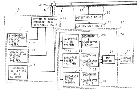
identifying apparatus ~~omprises a signal applying section 10
5 which applies a potential signal of specific frequency to
conductor A1 of particular cable A, and a signal detecting
section 20 which is provided in contact or not in contact with
particular cable A to detect the potential signal of the
specific frequency. The applying section 10 is spaced away
10 from the detecting sect=ion 20 with any distance; the detecting
section 20 detects the potential signal of the specific
frequency through an opened cover of the trough at any place
away from the applying section 10, and identifies particular
cable A among the cables which are housed.
15 The signal applying section 10 is comprised of an
oscillating circuit sec:t:ion 11, which issues potential signals
of different types (channels) of frequencies specified in
advance (hereinafter referred to as "frequency signals"), a
potential signal compounding & applying circuit 15 which
compounds those frequency signals and applies them to conductor
A1 of particular cable A, and a tool (clip) 16 which is
attached to the conductor A1 to apply the potential signals
received from the poter..tial signal compounding & applying
circuit 15 to conductor Al.
The oscillating circuit section 11 is comprised of,
for example, three sinusoidal oscillating circuits 12 through
14. The sinusoidal oscillating circuits 12 through 14 generate
three channels of sinusoidal potential signals of, for example,
875[Hz], 3.7[kHz], and 10[kHz], which are not normally used
3~J much. As the oscillating circuit section 11 according to the
present invention used in this embodiment, a circuit, which
generates, for example, a particular frequency signal at
regular time intervals, may alternatively be used.
CA 02113836 2001-06-12
72465-58
16
The potential signal compounding & applying circuit
15c compounds the frequency signals of the three channels and
issues a compound signal which has a waveform shown in FIG. 2.
The compound signal is applied to conductor A1 of particular
cable A via the clip 16.
The signal detecting section 20 is comprised of a
signal electrode 21 which consists of a metallic plate disposed
in the vicinity of particular cable A sheathed with an
insulator, a detecting circuit 22 which is connected to the
signal electrode 21 to detect the potential signals from
conductor A1, an amplifying circuit 23 which amplifies
potential signals and which permits adjusting the gain of
amplification, a signal identifying circuit 24 which identifies
particular cable A from the amplified potential signal, and a
display circuit 32 which indicates the identified particular
cable A.
In this detecting section 20, an extremely small
capacitance exists between the signal electrode 21 and the
conductor Al of the particular cable A. The potential of
conductor A1 is detected by this electrostatic coupling, and
therefore, the detecting circuit 22 uses a buffer circuit with
CA 02113836 2001-O1-16
72465-58
17
an extremely high input impedance; in this embodiment, a
voltage follower circuit, which employs, for example, a field
effect transistor (hereinafter referred to as "FET"), is used
to detect an input signal having a waveform as shown in Fig. 3.
'~ This input signal includes noise components of 50[Hz], for
example, and other frequencies in addition to the signal
frequency components of the three channels of 875[Hz],
3.7 [kHz) , and 10 [kHz] discussed above.
The detecting circuit 22 is comprised of an
electroscope equipped with a voltage follower circuit
consisting of, for exam le, J (Junction) FET operational
amplifier which has an extremely high input impedance.
Referring to FIG. 4, in the electroscope, the signal electrode
21 and an earthing electrode 22a, which are in contact with
1~> cable A via insulating :Layers 22b, consist of two metallic
plates, the insulating :Layers 22b existing between the signal
electrode 21 and the earthing electrode 22a. The earthing
electrode 22a has a sma:L:L hole 22c opened to let a lead wire
22d of the signal electrode 21 pass through it at its middle
2C portion. The lead wire 22d is connected to a positive input
terminal of a voltage follower circuit 22e comprised of the
JFET operational amplifier.
Referring to FIG. 5 which shows the equivalent
circuit of the electroscope of FIG. 4, the signal electrode 21
25 and the earthing electrode 22a constitute a capacitor 22g which
is connected in parallel_ to an input circuit 22f of the
electroscope. Its capacitance CIN is determined from the
following:
CIN = KE x 8 . 555 x 10'12 x Sid . . . ( 1 )
30 where S: Area of metallic plate
d: Thickness of insulating layer
KE: Die:lectric constant of insulating layer
CA 02113836 2001-O1-16
72465-58
18
In FIG. 5, Vs is the signal voltage applied to the
cable, VIN is an input voltage to the amplifying circuit, CA is
an electrostatic coupling capacitance between the signal
electrode and a cable conductor, RIN is an input impedance of
the input circuit 22f consisting of the voltage follower
circuit 22e, and 22h is a voltage applied.
The specific embodiment of the electroscope shown in
FIG. 4 will have a configuration as shown in FIG. 6 and FIG. 7
which is a sectional view taken on line 7-7 of FIG. 6. In FIG.
6 and FIG. 7, like parts are shown by the same reference
characters as in FIG. 4 for the convenience of explanation.
The same reference characters are also used for the convenience
of explanation in FIG. 8 through FIG. 13 to be discussed later.
Referring to FIG. 6 and FIG. 7, the signal electrode
1~~ 21, the insulating layers 22b, and the earthing electrode 22a
are all shaped rectangularly, and a cylindrical metallic plate
22i is fixed on the earthing electrode 22a. In the aforesaid
metallic plate 22i, the operational amplifier 22e is included
and molded with insulating resin 22j to improve the reliability
and safety of the electroscope.
In the embodiment shown in FIG. 6 and FIG. 7, the
area S of the metallic plates of the signal electrode 21 and
the earthing electrode 22a is 16 [mm] x 30 [mm] - 480 [mmz] .
Further, the insulating layers 22b use plastic films and the
2'~ thickness d is 0.5[mm] <~nd the dielectric constant KE is 2. In
this case, the capacitance CIN of a capacitor formed by the
signal electrode 21 and the earthing electrode 22a is
approximately 17[PF] from the formula (1).
The magnitude of capacitance CIN should be about ten
plus times to a few dOZE:Il times electrostatic coupling
capacitance CA. In this case, if the impedance of the
capacitance CIN is taken as ZIN , the relation of ZIN < impedance
CA 02113836 2001-O1-16
72465-58
19
Za of coupling capacitance CA is established, so that it is
obvious that the relation of ZjN « an input impedance RIN of
Input circuit 22f is e:~tablished. Accordingly, an approximate
value of input voltage VIN can be determined by:
VIN = VS ' ZIr,I ~ZIN + ZA)
The magnitude of impedance ZA is approximately a few
dozen times impedance ZIN, and therefore, input voltage VIN is
one few-dozenths of applied signal voltage Vs. As a result, it
becomes completely impossible to saturate the output voltage of
the input circuit 22f from a 50[Hz) noise. Of course, although
the signal voltage detected also becomes one few-dozenths, the
noise other than the signal voltage can be removed by band-pass
filters 25-27 which will. be described later. Further,
impedances ZIN and ZA also vary with the signal frequency;
therefore, input voltage VIN is independent of the signal
frequency making it convenient for the signal processing to be
discussed later.
In this embodiment, when a capacitor, which is
equivalently formed with the signal electrode and the earthing
2c) electrode, is connected in parallel to the input circuit and
the capacitance of the capacitor is adjusted to a dozen times
the electrostatic coupling capacitance, the magnitude of the
impedance of the electrostatic coupling capacitance becomes
about a dozen times the impedance of the capacitance of the
capacitor. Accordingly, the input voltage becomes one few-
dozenths of the applied signal voltage. Namely, a level of the
applied signal voltage from the signal applying section 10 has
a relationship proportional to a level of the signal voltage
detected in the signal detecting section 20. As a result, in
this embodiment, the sa1_uration of the output voltage of the
input circuit due to the 50[Hz] noise can be prevented, making
CA 02113836 2001-O1-16
72465-58
it possible to easily detect the frequency signals of the three
channels applied to the cable independently of frequencies.
The electroscope according to the present invention
is not limited to the embodiment shown in FIG. 6 and FIG. 7.
5 More specifically, as ;shown in FIG. 8, for instance, there is
also a version comprised of an earthing electrode and a
cylindrical metallic p:Late which are combined into one piece to
form a metallic case 2:?k.
As shown in FTG. 9, there is another version wherein
1.0 a plastic case 221 is attached to a signal electrode 21, the
inner wall of the plastic case 221 being provided with metallic
plating 22m.
As shown in F'IG. 10 and FIG. 11, which is a sectional
view taken along line 1.1-11 of FIG. 10, there is still another
15 version wherein the signal electrode 21 is formed into a disc
shape and a cylindrical. earthing electrode 22a is attached to
the signal electrode 21. via the insulating layer 22(b).
Further, as shown in FIG. 12 and FIG. 13, which is a
sectional view taken along line 13-13 of FIG. 12, the
20 electroscope may alternatively be a version wherein the signal
electrode 21, the insulating layer 22(d), and the earth
electrode 22(a) are curved so that the electroscope can be
closely attached to cable A which is the object to be subjected
to measurement.
The magnitude of the potential signal detected
through the detecting circuit 22 changes with the following
major causes:
(1) Distance between the signal electrode 21 and
conductor A1;
CA 02113836 2001-06-12
72465-58
21
(2) Dielectric constant of the insulating layer
material of particular cable A; and
(3) Input impedance of the detecting circuit 22.
Hence, to cope with such changes, an amplifying
circuit 23 is required to amplify input signals.
The amplifying circuit 23 has an important function
in addition to amplifying input signals; it is to locate a
particular cable out of a dozen cables housed in the same
trough. This amplifying circuit 23 is set so that the gain
(sensitivity) may be adjusted. To locate particular cables,
the gain of the amplifying circuit 23 is set to its maximum
level by adjusting a resistance of the variable resistor VR1,
and an approximate range wherein a particular cable A, to which
the compound signal is being applied, is present, is identified
in the trough. Subsequently, the gain is adjusted to an
appropriate level by changing a resistance of the variable
resistor VR1, and the cables existing in the range are checked
one by one to locate a particular cable A. This, in the
embodiment, saves the time and labor to check all the cables in
the trough one by one through the detecting section 20,
significantly saving work time.
The sensitivity indicates the greatest distance from
which the signal electrode 21 can identify target particular
cable A accurately. Specific practical equipment with a high
sensitivity can accurately identify particular cable A even
when the signal electrode 21 is a few centimetres away from
particular cable A.
CA 02113836 2001-O1-16
72465-58
22
The signal identifying circuit 24 comprises band-pass
filters 25 through 27, which let three types of particular
frequency signals, respectively, among the input signals
described above to pass through them, smoothing & comparator
circuits 28 through 30 which are connected to the band-pass
filters 25 through 27, and an AND circuit 31 which performs AND
operation in the comparison results received from the smoothing
& comparator circuits 28 through 30.
The band-pass filters 25 through 27 correspond to
sinusoidal oscillating circuits 12 through 14; and they detect
the frequency signals of the three channels, 875[Hz], 3.7[kHz],
and 10[kHz] generated by the sinusoidal oscillating circuits 12
through 14. The noise components contained in the input
signals are removed by the band-pass filters 25 through 27.
The smoothing & comparator circuits 28 through 30 are
provided corresponding to the band-pass filter 25 through 27.
The smoothing & comparator circuit 28, as shown in FIG. 32,
comprises two operational amplifiers 28a and 28b connected to
the band-pass filter 25 through a capacitor C2, diodes, D1 and
D2, and a comparator 28c connected through the operational
amplifier 28b and a resistor R4. The smoothing & comparator
circuit 29 comprises two operational amplifiers 29a and 29b
connected to the band-pa;~s filter 26 through a capacitor C3
diodes D3 and D4, and a comparator 29c connected through the
operational amplifier 29b and a resistor R5. The smoothing &
comparator circuit 30 comprises two series-connected
operational amplifiers 30a and 30b connected to the band-pass
filter 27 through a capacitor C4, diodes DS and D6, and a
comparator 30c connected through the operational amplifier 30b
and a resistor R6. These: operational amplifiers 28a, 28b, 29a,
29b, 30a, 30b and diodes D1 to D6 rectify and smooth the
frequency signals passin<~ through the band-pass filters 25
through 27. Moreover, the comparators 28c, 29c and 30c
CA 02113836 2001-06-12
72465-58
23
individually compare the smoothed frequency signals with a
specified reference signal. More specifically, the smoothing &
comparator circuits 28 through 30 judge whether the frequency
signal levels are higher or lower than the prescribed threshold
value levels which are preset in the circuits 28 through 30.
And if the frequency signal levels are higher than the
reference signal levels, then the smoothing & comparator
circuits 28 through 30 apply an output "1" to the AND circuit
31.
When the outputs from the three smoothing &
comparator circuits 28 through 30 are all "1", the AND circuit
31 gives the output "1". The output of the AND circuit 31
indicates that the frequency signals of the three channels
issued by the sinusoidal oscillating circuits 12 through 14
have been detected.
The display circuit 32 has a lamp and a buzzer which
are not illustrated and if the output of the AND circuit 31 is
"1", an LED lamp of the LED display section is lit, and the
buzzer drive section causes a buzzer to sound. By so doing,
the display circuit 32 indicates that the cable close to the
signal electrode 21 is particular cable A to which the
frequency signal has been applied.
Hence, in this embodiment, the signal applying
section applies three different frequency signals, which are
usually very unlikely to be used at the same time, to the
particular cable and the signal detecting section close to the
cable detects the frequency signals. This makes it possible,
in this embodiment, to efficiently identify a particular cable
without erroneous judgement, permitting improved reliability in
identifying cables.
CA 02113836 2001-O1-16
72465-58
24
Additionally, in this embodiment, the signal
detecting section is foamed by electrostatic coupling with
respect to the cables, making it possible to control the
currents, which are applied to the cables, to an extremely low
level. Therefore, when the identifying apparatus according to
this embodiment is used as a portable apparatus, the exhaustion
of the dry cells is reduced, making it an ideal portable
apparatus.
Further, in this embodiment, the amplifying circuit
with adjustable sensitivity is used; therefore, a particular
cable can be detected with high sensitivity even if the
distance between the electrode and a conductor increases,
permitting improved work efficiency.
The sensitivity of the signal detecting section for
locating a particular cable can be increased by increasing the
gain of the amplifying circuit 23 as discussed above. The
present invention, however, is not limited to that; the
sensitivity of the signal detecting section can be increased
by, for example, lowering the threshold value levels of the
reference signals of the smoothing & comparator circuits 28
through 30.
Further, in this embodiment, three different
frequency signals are compounded to provide the compound
signal, however, the present invention is not limited to that;
two or four or more different frequency signals may be
compounded to provide the=_ compound signal.
Furthermore, objects to be measured can be identified
by the present invention as long as they are electrically
conductive lengthy objects including iron pipes, iron-wire-
armoured plastic pipes consisting of plastic pipes wrapped with
iron wires, steel-stranded wires (steel wires) used as the
tension wires for bridge: and the like, and fluid transport
CA 02113836 2001-O1-16
72465-58
tubes reinforced with metals, in addition to cables such as
regular electric wires.
The following discusses how each of a plurality of
cables housed in a trough is identified.
FIG. 14 is the block diagram showing the
configuration of the identifying apparatus which employs the
second embodiment of the. identifying method for objects to be
identified according to the present invention. Referring to
FIG. 14, the identifying apparatus comprises a signal applying
10 section 40, which applies potential signals of a plurality of
combined specific frequencies to the cable conductors sheathed
with insulators, and a signal detecting section 50 which is
provided in contact or not in contact with one of the cables,
e.g. cable A, and which detects the potential signal of the
15 specific frequency. As in the first embodiment, the applying
section 40 is spaced away from the detecting section 50 with
any distance; as soon as. the detecting section 50 identifies a
cable, it detects the potential signal of the specific
frequency of another cable through contact or no contact with
20 the cable, thus identifying all cables housed in a trough one
by one.
Referring to FIG. 15, the signal applying section 40
comprises an oscillating circuit section 41 which generates six
different preset channels of frequency signals fl through f6, a
25 compounding circuit 42 which compounds signals of three
channels of different combinations from the frequency signals,
applying circuits 43a through 43t which apply the composite
signals to the conductors of the cables which are defined in
advance, and clips, 44a through 44t which are attached to the
conductors to apply the composite signals from the applying
circuits 43a through 43t to the conductors.
CA 02113836 2001-O1-16
72465-58
26
The oscillating circuit section 41 comprises
sinusoidal oscillating circuits 41a through 41f which are the
signal sources for generating sinusoidal potential signals of,
for example, six channe7_s of frequencies fl through f6 which
are not usually used much.
The compounding circuit 42 compounds three types of
signals of different combinations from the six received
different frequency signals and outputs them. A number K of
the different combinatic>ns can be determined by the following
formula:
K = N! /M! ~ (I~f-M) ! . . . (2)
where N: Number of signal sources
M: Number of composite samples
In the case of this embodiment, N=6 and M=3;
therefore, substituting these values for the formula (2)
results in K=20. This means that, in this embodiment, up to
twenty cables can be identified at a time. Accordingly, in
this embodiment, twenty applying circuits and twenty clips are
required.
The signal detecting section 50 comprises a signal
electrode 51 which consists of a metallic plate disposed near
particular cable A sheathed with an insulator, a detecting
circuit 52 which is connected to the signal electrode 51 and
detects a potential signal from conductor A1, a signal
identifying circuit 53 which identifies a cable according to a
detected potential signal, and display circuits 57a through 57t
which indicate identified cables.
In the detecting section 50, the detecting circuit 52
comprises an electroscope equipped with a voltage follower
circuit consisting of a ,JFET operational amplifier because of
the same reason as the first embodiment and it detects input
signals.
CA 02113836 2001-O1-16
72465-58
27
The signal identifying circuit 53 comprises signal
processing circuits 54a through 54f which carry out prescribed
signal processing on detected potential signals, a combining
circuit 55 which combines the six processed outputs CH1 through
CH6, three each, and AD1D circuits 56a through 56t which perform
AND operation on the combined outputs, three each.
Each of the ~;ignal processing circuits channels 54a
through 54f of six channels comprises an amplifying circuit
which is provided because of the same reason as the first
embodiment and which is not illustrated, a band-pass filter
which allows a particular frequency signal among input signals
to pass through, and a smoothing & comparator circuit which
smoothes the frequency signals, which have passed through the
band filters, and compares the frequency signals with reference
1.'~ signals.
The band-pass filters correspond to the sinusoidal
oscillating circuits 41a through 41f and their central
frequencies are preset so that they are equivalent to the six
different signal frequencies fl through f6 which are generated
by the sinusoidal oscillating circuits 41a through 41f.
Therefore, noise components contained in input signals are
removed by the band-pass filters.
The smoothing ~ comparator circuits are provided so
that they correspond to the band-pass filters, and as in the
2~~ case with the first embodiment, they compare the smoothed
frequency signals with the threshold value levels of the
reference signals. If the frequency signals are larger than
the reference signals, t=hen the smoothing & comparator circuits
set the outputs CH1 through CH6 applied to the combining
circuit 55 to "1".
CA 02113836 2001-O1-16
72465-58
28
The combining circuit 55 combines the six outputs CHl
though CH6, which have been processed by the signal processing
circuits 54a through 54f=, three each as in the case of the
compounding circuit 42 and supplies them to the AND circuits
56a through 56t.
If all the three outputs from the combining circuit
55 are "1", then the ArID circuits 56a through 56t set their
outputs to "1". These AND circuits 56a through 56t correspond
to the applying circuits 43a through 43t, and the outputs of
the AND circuits 56a through 56t indicate that the three
different frequency signals applied to the cables by the
applying circuits 43a through 43t have been detected.
Display circuits 57a through 57t have lamps, which
correspond to the AND circuits 56a through 56t and which are
not illustrated, and they indicate operation results. More
specifically, in the display circuits S7a through 57t, if the
output of any of the AD1D circuits 56a through 56t is "1", then
the display circuit whi_c:h corresponds to the AND circuit causes
its lamp to light to show which number of cable is the one
approximate to the signal electrode 51.
In this embodiment, up to twenty cables can be
identified at the same time; therefore, twenty AND circuits and
twenty display circuits are required.
The operation of the identifying apparatus shown in
FIG. 14 and FIG. 15 wi7.1 now be described. In Fig. 14,
particular cable A to be identified will be the ninth cable Ai
and the electrode 51 will be brought close to cable Ai.
The clips 44a through 44t of the signal applying
section 40 are attached to the conductors of the cables in the
trough, the ninth clip 44i being attached to the conductor of
cable Ai.
CA 02113836 2001-O1-16
72465-58
29
Under such a condition, the compounding circuit 42
compounds three different frequency signals, f3, f4 and f5,
issued from the oscillating circuits 41c through 41e out of the
sinusoidal waves fl through f6 issued from the sinusoidal
'.~ oscillating circuits 41a through 41f and supplies the result as
the compound signal (see FIG. 2) to the applying circuit 43i.
The applying circuit 43i then applies the compound signal of
the frequency signals f3, f4, and f5 to the conductor of the
ninth cable Ai via the clip 44i.
This enables the signal detecting section 50 to
detect the compound signal. Specifically, the input signal
from particular cable Ai is detected by the detecting circuit
52 via the electrode 51, which is disposed in the vicinity of
cable Ai, the input signal exhibiting a waveform which contains
1'. the three different frequency components, f3, f4 and f5, and
other noise components (see FIG. 3). The input signal is
applied to the individual signal processing circuits 54a
through 54f of six channels; according to the frequency
components of the input signal, outputs CH3 through CH5 of only
2G the signal processing circuits 54c through 54e, which
correspond to the sinusoidal oscillating circuits 41c through
41e, become "1"
The combining circuit 55 combines the outputs CH3
through CH5 received from the signal processing circuits 54c
2~ through 54e and supplier the result to an AND circuit 56i.
This causes the output of only this AND circuit 56i to become
"1". The output from the AND circuit 56i causes the display
circuit 57i, which is connected to the AND circuit 56i, to
light the lamp, thus indicating that the cable to which the
30 signal electrode 51 is close to the ninth cable Ai. Then,
bringing the electrode 51 close to other cables in sequence
makes it possible to ide=_ntify all cables in the trough as in
the case described above..
CA 02113836 2001-O1-16
72465-58
The influences exerted by the electrostatic coupling
capacitance among the cables in the trough will now be
discussed.
There is electrostatic coupling capacitance also
'~ among the cables in this trough and it may be well over the
electrostatic coupling capacitance between the electrode and
the cables. For this reason, to identify the cables, the
mutual influences among the cables must be taken into account.
FIG. 16 shows the equivalent circuit which involves
10 cables A and B set as an example to explain the influences
exerted by the electrostatic coupling capacitance among the
cables. In this example, the impedance of the electrostatic
coupling capacitance between cables A and B is denoted as Rc,
and the impedances between cables A and B and the earth via the
15 applying circuit are denoted as Ra and Rb, respectively.
Thus, the signal voltage applied to cable A is Va and
the signal voltage Va exerts influences on cable B via the
coupling capacitance between cables A and B. If the signal
voltage of cable B is denoted as Vb, then Vb can be determined
20 by:
Vb = Va ~ Rb / ( Rb + Rc )
In actual use, if Rc » Rb, then Vb « Va. This
means that if the impedance among the cables is sufficiently
small, then the influences exerted by the coupling capacitance
2~~ among the cables will be small enough to be ignored.
Hence, in this embodiment, the signal applying
section applies three types of frequency signals in different
combinations out of the six different frequency signals, which
are usually very unlikely to be used at the same time, to each
30 of the cables, and the signal detecting section close to the
CA 02113836 2001-O1-16
72465-58
31
cable detects the frequency signals. Thus, in this embodiment,
a plurality of cables can be efficiently identified without
making erroneous judgement, permitting higher reliability of
identifying cables.
Further in this embodiment, the signal detecting
section is formed by electrostatic coupling with respect to the
cables, and therefore, the same effect as that in the first
embodiment will be acquired. Moreover, in this embodiment, the
work for attaching identifying labels to the cables is no
1~ longer necessary, allowing cables to be easily identified by a
single worker.
The display circuit in this embodiment can be
considered in various configurations. For example, a
configuration is considered wherein outputs of the signal
1~ processing circuits are supplied to a particular decoder
circuit and the number of a channel, the output thereof has
become "1" through the decoder, is displayed on a LCD panel.
This allows the LCD panel to directly display the number of the
cable by this channel number.
20 Incidentally, in an actual trough, a few dozen of
cables to be identified are usually present in an extremely
disorderly manner and there is electrostatic coupling among the
cables. And in some cases, the capacitance between adjoining
cables is larger than tr:e capacitance which exists between the
25 signal electrode of the detecting section and a particular
cable to be identified. In such a case, in the identifying
method of the first embodiment described above, the influence
exerted by the capacitance between the cables causes an applied
signal to be detected also from a cable adjacent to the
30 particular cable. This. makes it impossible to detect the
particular cable out of the cables to be identified.
CA 02113836 2001-O1-16
72465-58
32
To solve such a problem, the third embodiment
according to the present invention shows an identifying method
which is not influenced by the capacitance between cables when
identifying a particular cable.
FIG. 17 through FIG. 22 show the principle diagrams
of typical three different situations and their equivalent
circuits assumed to explain the principle of the embodiment.
Referring to these drawings, the influences exerted by the
capacitance among cables will be theoretically analyzed. In
1() FIG. 17 through FIG. 22, the same parts as those of FIG. 1 are
shown by the same reference characters for the convenience of
explanation.
Referring to FIG. 17 through FIG. 22, A through D are
the cables to be identified and cable A is the particular cable
15 to be identified. FIG. 17, FIG. 19 and FIG. 21 show the cross-
sectional views of cables A through D. Cables A through D are
comprised of conductors A1 through D1 and shielding layers A2
through D2. These cables A through D are supposed to be laid
in parallel against each other lengthwise. In all these
2U drawings, all the coupling capacitances between adjoining
cables are denoted as CT and the impedances as Z likewise for
simplicity for the convenience of explanation.
First, a case wherein particular cable A is detected
in FIG. 17 and FIG. 18 will be explained.
25 Referring to FIG. 17, the earthed oscillating circuit
section 11 directly applies a potential signal of a given
voltage (hereinafter referred to as "voltage signal"), e.g.,
signal voltage ~Vs, to conductor A1 of particular cable A. The
detecting section 20 utilizes the electrostatic coupling
3.) capacitance CA between conductor A1 of cable A and the signal
electrode 21 to detect the voltage signal. In this case, the
impedance of the coupling capacitance CA is denoted as Z~A, an
CA 02113836 2001-O1-16
72465-58
33
input impedance of the detecting circuit 22 to be discussed
later is denoted as ZIN, and the detection voltage of the
voltage signal is denoted as VIN. If ZIN « ZcA to actually
prevent VIN from being saturated, then the detection voltage VIN
!~ is determined by the following formula from the equivalent
circuit shown in FIG. 18:
VIN = VS ' ZjN ,/ (ZIN t Z~~)
- Vs ' Zirr / Zca . . . ( 3 )
The detecting section 20 determines whether a cable
is particular cable A at the level of the signal voltage of
three different frequencies (hereinafter referred to as
"frequency signal") which are contained in a detected signal.
In other words, it determines whether the cable is particular
cable A according to the magnitude of the detection voltage VIN.
1> One of the important conditions to make the signal
voltage Vs sufficiently high is that none of conductor A1 of
particular cable A, shielding layer A2, and the armor are
earthed. This is because the signal potential level of cable A
would approximate to zero due to the influence of an internal
impedance (normally approximately SO f2) of the oscillating
circuit section 11 unless the conductive part to which the
signal voltage Vs is applied is isolated from the earth. As a
result, detection voltage VIN would also approximate to zero,
making it impossible to identify particular cable A.
2~i Next, a case will be explained wherein particular
cable A and cable B, which has a large coupling capacitance,
are identified in FIG. 19 and FIG. 20.
Referring to FIG. 19, cable B is adjacent to
particular cable A and it is earthed, with its impedance
denoted as ZB. In this equivalent circuit shown in FIG. 20, the
electrostatic coupling capacitance between conductor B1 of
CA 02113836 2001-O1-16
72465-58
34
cable B and the signal electrode 21 is denoted as CB and the
impedance as ZcB. The detection voltage VIN in this case is
determined by the following formula (utilizing ZIN « ZcB)
VIN = C ZB ' ZcB~ { Z ( ZB + ZcB ) + ZB ' ZcB } ~
CVs ' ZIN~zCB~
. . (4)
Impedances Z and ZcB depend on the arrangement of
cables in a trough and they cannot be changed artificially.
Hence, the value of detection voltage VIN greatly varies
according to impedance ZB. A cable in service is earthed, and
therefore, it is obvious that impedance ZB « ZcB and ZB « Z.
Detection voltage VIN determined in formula (4) can be
simplified as follows:
VIN = (zB~Z) ' (US ' ZIN~ZCB) . . . (5)
1'.~ VIN of formula. (5) « VIN of formula (3) ; therefore,
even if the signal electrode 21 touches cable B, the detecting
section 20 can securely distinguish particular cable A from
cable B because detection voltage VIN from cable B is extremely
low.
One of the important conditions to make the detection
voltage VIN of the cables other than the particular cable
sufficiently low is to securely earth the oscillating circuit
section 11. This is because impedance ZB contains the impedance
between the oscillating circuit section 11 and the earth. If
2.'~ the oscillating circuit section 11 were not earthed, then
detection voltage VIN would be generated each time the signal
electrode 21 touches a cable.
Thus, in the case discussed above, detection voltage
VIN is generated because impedance ZB approximates to infinity
3) and the cables in a trough are extremely long, causing the
CA 02113836 2001-O1-16
72465-58
coupling capacitance among the cables to grow sufficiently
larger than electrostatic coupling capacitance CH. The result
is ZB » Z, Z$ » Z~B, Z « Z~B, and detection voltage VIN of
formula (4) can be simplified as follows:
S VIN - VS ' ZIN ~ (zCB '~ ZIN)
- Vs ' ZIN ~ zCH . . . (6)
The value of VIN of formula (6) is approximately the
same as that of VIN of Formula (3). Hence, the particular cable
cannot be identified.
10 A case will now be described wherein particular cable
A is identified when cable B is not in service. In this case,
when the trough has two cables, A and B, in ir_, impedance ZB
shown in FIG. 19 and Fi.g. 20 approximates to infinity. This is
the same situation as that represented in formula (6);
15 therefore, it is difficult to securely distinguish cable A from
cable B. To avoid this;, the conductor of cable B is earthed to
approximate impedance 2.H to zero. Thus, detection voltage VIN
from cable B also apprc>ximates to zero, making it easy to
distinguish particular cable A from cable B. Accordingly, in
20 this case also, one of the important conditions to make
detection voltage VIN Oj= cable B not in service other than the
particular cable sufficiently low is to earth cable B.
Actual situations are, however, more complicated and
there are a dozen of cables in a trough, most of them being in
25 service. It is also not easy to earth all cables that are not
in use. To solve such a problem, according to the present
invention, the situation of an embodiment shown in FIG. 21 and
FIG. 22 will be discus~;ed. In this embodiment, there are
cables A and B, which a.re not used, in the trough, and the two
30 cables are arranged side by side, both having large coupling
capacitances. It is a~;sumed that cables C and D, which exist
around cables A and B, are all in service. Under such a
CA 02113836 2001-O1-16
72465-58
36
condition, it is assumed that the impedance between cable C and
the earth is expressed as Z~ and the impedance between cable D
and the earth is expressed as ZD, and the coupling capacitance
between cables B and C, and between cable B and D is expressed
as CT, the impedance being expressed as Z.
In this case, in the equivalent circuit shown in FIG.
22, cables C and D in ~,ervice will have Z~ « Z, Zp « Z, and
impedances Z~ and ZD area ignorable; therefore, the relationship
between voltage VB of cable B and signal voltage VS and the
relationship between detection voltage VIN and signal voltage VS
will be as shown below:
Ve _ VS ~ Zca ( + 3 Z~H ) . . . (
/ Z 7 )
VIN - { zCEi( '+ 3 ZCH ) ? ' ZIN/
US ~ / Z ZCB
US ~ ZIN (Z + 3ZCB) . . . (8)
/
1S Formula (3) a.nd formula (8) have proven that the
level of detection voltage VIN from cable B is one third or less
of the level of detection voltage VIN from the particular cable.
Hence, even if cable B not in service is not earthed, the level
of detection signal VIr, from cable B is one third or less of the
level of detection signal VIN from the particular cable because
of the influences of th.e surrounding cables in service; in this
case, appropriately adjusting the sensitivity of the detecting
section 20 makes it possible to identify particular cable A.
Based on this verification, in the present invention,
when a particular cable: is identified using, for example, an
electrostatic coupling type cable identifying apparatus shown
in FIG. 23, the following conditions will be used:
(1) A cable to be removed is isolated from a
connection terminal or the earth.
CA 02113836 2001-O1-16
72465-58
37
(2) If there is a cable not in use in an oscillating
circuit or a trough to work on, then the shielding layer of the
cable (the conductors of the bundled cables if there is no
shielding layer) is earthed.
(3) However, if there is any special situation, then
a particular cable will be identified by adjusting the
sensitivity of the detecting section to be discussed later
without earthing.
FIG. 23 is the block diagram which shows the
configuration of an identifying apparatus which employs the
third embodiment of the: cable identifying method according to
the present invention a,=~ described above. In FIG. 23, the same
parts as those shown in FIG. 1 use the identical reference
characters for the convenience of explanation.
In the diagram, particular cable A is comprised of
shielding layer A2 and conductor A1 which is insulated with the
shielding layer A2 and it is isolated from the earth in
accordance with condition (1). Likewise, the cables other than
particular cable A, which are present in the trough, are
earthed in accordance with condition (2) when they are not in
service.
The identifying apparatus consists of the signal
applying section 10, which applies a frequency signal of a
particular frequency to conductor A1 of particular cable A, and
the detecting section 20 which detects the signal voltage of
the applied frequency ~~ignal in contact or not in contact with
housed particular cable A through an opened cover of the trough
at any distance from the signal applying section 10, thereby
identifying the cable.
The signal applying section 10, as in FIG. 1, is
comprised of sinusoida7_ oscillating circuits 12 through 14
CA 02113836 2001-O1-16
72465-58
38
consisting of the oscillating circuit 11, the voltage signal
compounding & applying circuit 15 which compounds these
frequency signals and applies the resultant voltage signal to
conductor A1 of particular cable A, and the clip 16 which is
attached to conductor P,1 and which applies the voltage signal
from the voltage signal. compounding & applying circuit 15 to
conductor A1. In this case, the clip 16 may be connected to
shielding layer A2.
The sinusoidal oscillating circuits 12 through 14 are
earthed in accordance with condition (2) and generate three
different sinusoidal frequency signals of, for example,
875 [Hz] , 3 . 7 [kHz] , and 10 [kHz] which are normally not used
much.
The detecting. section 20 is comprised of the
detecting circuit 22, the amplifying circuit 23 which amplifies
a voltage signal and allows the amplifying gain to be adjusted
in accordance with condition (3), the signal identifying
circuit 24 which identifies particular cable A from the
amplified voltage signal, and the display circuit 32.
The amplifying circuit 23 amplifies a voltage signal
to cope with a change in the magnitude of the voltage signal
detected by the detecting circuit 22. The amplifying circuit
23 has another important function; it is to locate a particular
cable out of a dozen cables that are present in the same
trough, and the amplifying circuit 23 is designed to permit the
adjustment of gain (the adjustment of sensitivity) for
accomplishing the fun<::ti.on.
The sensitivity is a judgement standard for the level
of detection signal VIN,, and the higher the sensitivity, the
lower the required signal level of detection signal VIN. In
other words, the sensitivity indicates the greatest distance
from which the signal electrode 21 can accurately identify
CA 02113836 2001-O1-16
72465-58
39
particular cable A. In the case of specific practical
equipment, if the sensitivity is high, then the detection
signal is generated even when the signal electrode 21 is
slightly away from particular cable A, thus making it possible
!~ to identify particular cable A without the need of adjusting
the sensitivity. However, as shown in condition (3), if a
cable not in service exists and if the cable can not be
earthed, then it may be impossible to distinguish the cable not
in use from the particular cable. For this reason, it is
li) essential to properly adjust the sensitivity of the amplifying
circuit 23 in accordance with condition (3).
As a sensitivity adjusting mechanism for the
amplifying circuit 23, the following two embodiments, for
example, are conceivable:
1~~ (Embodiment 3-1)
A sensitivity adjusting mechanism is considered,
wherein a control knob for continuously adjusting the detection
sensitivity is provided and the sensitivity level which is set
through this control knob is continuously displayed on an LCD
20 panel. In this example, when the panel shows that the
sensitivity has been set, for example, to 0.3V, if the level of
a detected signal exceeds 0.3V, then a specified visual or
audio detection signal for example, is given.
(Embodiment 3-2)
25 Another example is considered, wherein the
sensitivity is adjusted in rotary steps. In this example, the
sensitivity is ranked into 1 to 6, for instance, and the signal
levels for generating the detection signals are set to 0.3V,
0.6V, 1.2V, 2.4V, 4.8, and 9.6V according to the six ranks to
30 detect signals.
CA 02113836 2001-O1-16
72465-58
The signal identifying circuit 24 is comprised of the
similar band-pass filters 25 through 27, smoothing & comparator
circuits 28 through 30, and the AND circuit 31 to those shown
in FIG. 1, and it performs the similar operation to that shown
5 in FIG. 1.
The following presents detailed description of a
method for adjusting the sensitivity by using the sensitivity
adjusting mechanism of_ Embodiment 3-2.
First, the signal voltage is applied to the
10 particular cable through the signal applying section 10, then
the sensitivity adjustment of the amplifying circuit 23 of the
detecting section 20 i~~ performed. In this case, the
adjustment should be carried out in the vicinity of the signal
voltage applying place where it is possible to determine
15 whether the cable with which the signal electrode 21 is in
contact is particular cable A.
The first step of this sensitivity adjusting
procedure is to set the sensitivity to rank 1 and bring the
signal electrode 21 inta contact with all cables.
20 If the detecting section 20 issues no detection
signal for any of the cables, then the voltage applied to
particular cable A and isolation from the earth are examined.
Or, if the detection signal generated from the detecting
section 20 is only for particular cable A, then the sensitivity
25 is set to rank 3 and cc>ntact is made to particular cable A.
If the detecting section 20 issues a detection
signal, then it means that the sensitivity is appropriate;
therefore, the sensitivity adjustment is terminated. Or, if no
detection signal is prc>duced, then the sensitivity adjustment
30 is continued by raising the sensitivity rank until the
detection signal is is~;ued.
CA 02113836 2001-O1-16
72465-58
41
If the detecting section 20 issues the detection
signal for more than one cable, it indicates that the cable or
cables other than particular cable A are not in service and are
not earthed. In this case, the sensitivity rank is lowered
until the detecting section 20 generates the detection signal
only for particular cab7_e A to begin with. For instance, if
the then rank is 3, the sensitivity rank is lowered further by
two ranks to S before checking whether the detecting section 20
issues the detection signal for particular cable A.
If it has been proved that the particular cable can
be identified by the detecting section 20, the sensitivity
adjustment is finished. If any particular cable cannot be
identified, then the conductive portion or portions of a cable
or cables not in service are securely earthed.
After finishing the work described above, particular
cable A is identified in a desired trough; the cables, which
are present in the trough, are checked one by one to locate
particular cable A. This eliminates the need of checking all
the cables one by one, resulting in a dramatically reduced work
time.
Thus, in this embodiment, the signal voltage is
applied by the earthed :~.ignal applying section to the unearthed
particular cable and the signal voltage is detected by the
electrostatically detecting section with its gain adjusted.
2~~ Therefore, in this embodiment, the signal voltage is not
detected from any cable: other than the particular cable,
permitting accurate identification of the particular cable
without suffering from erroneous judgement.
As described <~bove, the sensitivity of the detecting
section for locating a particular cable can be increased by
increasing the gain of the amplifying circuit 23, however, the
present invention is not limited to that; alternatively, for
CA 02113836 2001-O1-16
72465-58
42
instance, the threshold value levels of the reference signals
of the smoothing & compai-ator circuits 28 through 30 may be
adjusted, namely, lowered to increase the sensitivity.
Next, the signal levels of the cables that are
present in an actual trough are detected, an example of
detection results being shown in the following Table 1 through
Table 3. Table 1 through Table 3 show the signal levels which
have been detected from f=our cables including the particular
cable in a place where the particular cable is laid.
Specifically, Table 1 shows the measurement results obtained in
the vicinity of the signal applying spot, Table 2 shows the
measurement results obtained at a terminal box located
approximately 560m away, and Table 3 shows the measurement
results obtained in a trough which is approximately 560 away.
Table 1
Signal Level
[V]
875[Hz] 3.7[kHz] 10[kHz]
Particular Cable 5.7 8.4 7.7
Cable 1 1.2 2.3 6.4
Cable 2 0.1 0.4 1.2
Cable 3 1_2 2.0 4.6
Table 2
Signal Level [V]
875[Hz] 3.7 [kHz] 10[kHz]
.Particular Cable 2.1 2.8 2.4
Cable 4 1.9 0.6 0
Cable 5 1.0 0.1 0
Cable 6 0.5 0.1 0.3
CA 02113836 2001-O1-16
72465-58
43
Table 3
Signal Level [V]
875[Hz] 3.7[kHz] 10[kHz]
Particular Cable 7.0 7.0 5.0
Cable 7 0.3 0 0
Cable 8 2.2 2.0 0.1
Cable 9 1.6 0.8 0
As it is obvious from the detection results, the
absolute values of the ~>ignal levels detected from the
particular cable significantly vary depending on the detection
spot.
Such variation is considered due to the difference in
the distance between the signal electrode and the conductor of
the particular cable, the difference in the dielectric constant
of intermediate materials or the like. As a result, in such a
case, it becomes necessary to adjust the sensitivity (the
magnitude of the threshold value of the comparator circuit) for
each detection spot. It: is possible to identify the particular
cable by adjusting the =sensitivity, however, the sensitivity
adjustment may adversely affect the reliability which must be
high in this identifying method.
To solve such a problem, in the fourth embodiment, an
identifying method is pi-ovided, wherein a particular cable
requiring no sensitivity adjustment can be identified even when
the signal level of the particular cable in the trough changes.
In this embodiment, three types of frequency signals (875[Hz],
3.7[kHz], and 10[kHz]) sharing the same amplitude are
compounded and applied as the voltage signal to the particular
cable.
The influences exerted by the capacitance among the
cables will now be explained theoretically. The proportional
CA 02113836 2001-O1-16
72465-58
44
relationship of the signal levels of the frequency signals
detected from the particular cable shown in Table 1 obviously
differs from the propori~ional relationship of the signal levels
of the frequency signal; detected from other cables 1 through
~~ 3. More specifically, :referring to Table 1, the signal levels
of the three channels detected from the particular cable are
almost the same, while the signal levels detected from other
cables significantly va:ry.
When the sign<~1 levels, 875 [Hz] , 3 . 7 [kHz] , and
10 [kHz] , are taken as V:1 [V] , V2 [V] , and V3 [V] , the trend of the
variations will be:
V1 [V] < V2 ['J] < V3 [V] . . . (9)
Theoretically, the cause for the different
proportional relationships can be explained as set forth below.
The signal voltage is directly applied to the particular cable;
therefore, the proportional relationship of the levels of the
frequency signals which the detecting section detects from the
particular cable is nearly the same as the proportional
relationship of the frequency signals before the oscillating
section compounds the signals. In contrast with this, the
levels of the frequency signals induced in the cables other
than the particular cable depend on a potential dividing
relationship shown below:
VY = ZAC ' Vs % ( Zac f Zcc ) . . . ( 10 )
2> where VY: Level of the voltage signal induced in
other cable
Vs: Level of the voltage signal applied to
the particular cable
ZAC: Impedance of other cable against the
3c) earth (Impedance of the capacitance)
CA 02113836 2001-O1-16
72465-58
Zcc: Impedance between other cable and the
particular cable (Impedance of the
capacitance)
The capacitance between other cable and the
5 particular cable is relatively stable and nearly identical
capacitance is given for the 10[kHz] signal. The capacitance
impedance between other' cable and the earth is considered to
tend to increase as the signal frequency increases. As a
result, the phenomenon shown in formula (9) takes place.
10 If ZAC « Zcc, then VY « VS and the signal level
detected will be 0[V] or extremely low. Referring now to Table
2 and Table 3, the data on the signal levels detected from
other cables 4 through 9 indicate different variations. Some
of the data, however, include those, the signal levels thereof
15 are 0[V] or extremely low. The cause for such data to have
been detected is considered due to noises rather than induced
signals. When detecting the particular cable, it is almost
impossible that the three specific frequency noises exist in
other cables at the same time. Hence, of the three channels of
20 the signal levels, at least one has a value which is
approximate to 0[V]. T'his can be found even by the identifying
method of the first emb~adiment discussed above.
Referring to Table 1, however, the data on the signal
levels detected from other cables 1 through 3 shows no signal
25 level which is 0[V] or extremely low. The fourth embodiment
shows a method which allows a particular cable to be identified
even in the case shown in Table 1.
FIG. 24 is a block diagram which shows the
configuration of the cable identifying apparatus which employs
30 the fourth embodiment of the method for identifying an object
to be identified according to the present invention. In FIG.
24, the like parts are shown by the same reference characters
CA 02113836 2001-O1-16
72465-58
46
as in the first embodiment of FIG. 1, and detailed explanation
will be omitted.
Referring to FIG. 24, the cable identifying apparatus
is comprised of the signal applying section 10, which applies a
frequency signal of a specific frequency to conductor A1 of
particular cable A sheathed with an insulator, and the
detecting section 20 which detects the signal voltage of the
applied frequency signal in contact or not in contact with
particular cable A at a point away from the signal applying
section 10, thereby identifying the cable.
As in the first embodiment, the signal applying
section 10, is comprised of the oscillating circuit section 11
consisting of the sinusoidal oscillating circuits 12 through
14, the voltage signal compounding & applying circuit 15, and
1!~ the clip 16, and the sinusoidal oscillating circuits 12 through
14 are all earthed and they generate three channels of
sinusoidal frequency signals of 875 [Hz] , 3.7 [kHz] and 10 [kHz] .
As in the first embodiment, the detecting section 20
is comprised of the signal electrode 21, the detecting circuit
22, the amplifying circuit 23, the signal identifying circuit
24, and the display circuit 32.
The signal identifying circuit 24 is comprised of the
band-pass filters 25 through 27 and the AND circuit 31, which
are similar to those in the first embodiment, and also AC/DC
2'~ converting circuits 60 through 62, DC voltage meters 63 through
65, and comparator circuits 66 through 68 which are provided
corresponding to the band-pass filters 25 through 27.
The AC/DC converting circuits 60 through 62 subject
the frequency signals of the three channels, which have passed
3~ through the band-pass filters 25 through 27, to AC/DC
CA 02113836 2001-O1-16
7246s-58
47
conversion and supply the results to the corresponding DC
voltage meters 63 through 65.
The DC voltage meters 63 through 65 detect the
voltage values V1, V2 a.nd V3 of the signals, which have been
converted through the converting circuits 60 through 62, and
supply them to the corresponding comparator circuits 66 through
68. To be specific, th.e DC voltage meter 63 detects the
voltage value V1 of the: frequency signal having a frequency of
875[Hz], the DC voltage: meter 64 detects the voltage value V2
of the frequency signal having a frequency of 3.7[kHz], and the
DC voltage meter 65 detects the voltage value V3 of the
frequency signal having a frequency of 10[kHz].
The comparator circuits 66 through 68 compare the
voltages V1, V2, and V3 of the frequency signals, which have
undergone the DC signal. conversion, with specified voltages.
More specifically, the comparator circuits 66 through 68
determine whether the voltages V1, V2, and V3 of the frequency
signals are higher or lower than the specified threshold value
levels that are preset in the circuits 66 through 68. If the
frequency signals are larger than the reference signals, then
the comparator circuit; 66 through 68 set the outputs supplied
to the AND circuit 31 t:o "1".
As in the first embodiment, if the outputs from the
three comparator circuits 66 through 68 are all "1", then the
AND circuit 31 sets its output to "1". When the output of the
AND circuit 31 is "1", the display circuit 32 indicates that
the cable to which the signal electrode 21 is approximate is
particular cable A to which the frequency signal has been
applied.
The following describes judgment standards for
particular cables in the signal identifying circuit 24, i.e.,
CA 02113836 2001-O1-16
72465-58
48
the standards for setting threshold values in the comparator
circuits 66 through 68.
First, the threshold values in the comparator
circuits 66 through 68 are established quantitatively and
qualitatively as shown below by utilizing the trend of the
variations in the signal levels of the three channels
discovered in experiments. In this example, the setting
standards for the threshold values in the comparator circuits
66 through 68 are established as follows:
V1 [V] > V3 [V] /m . . . ( 11 )
V2 [V] > V3 [V] /n . . . (12)
V3 [V] > VREF . . . ( 13 )
where m, n: Specific proportional constants
UREF~ Preset minimum reference signal level
1~> Inequalities (11) and (12) may be said to be
qualitative judgment standards which are determined by a mutual
proportional relationship of the three channels of signal
levels, V1, V2, and V3. Although inequality (13) is a
quantitative judgment standard, the objective of establishing
this standard is to provide a measure against noises.
In this embodiment shown in FIG. 24, for instance,
the "m" and "n" are set to 3 and 2, respectively, with VREF set
to 0.5[V], and only when all three inequalities (11) through
(13) are satisfied, a cable is identified as the particular
2!~ cable .
Under the condition, the signal levels detected from
the cables shown in Table 1 will be verified. In this case,
the signal levels detected from a particular cable by the
detecting section 20 satisfy inequalities (11) through (13) set
CA 02113836 2001-O1-16
72465-58
49
in all the comparator circuits 66 through 68 of the signal
identifying circuit 24, but the signal levels detected from
other cables 1 through :3 do not satisfy the inequalities.
Further, according to the verification results on the cables
shown in Table 2 and Table 3, as in the case with Table 1, only
the signal levels detec~'ed from the particular cable satisfy
inequalities (11) through (13) and the signal levels detected
from other cables 1 through 3 do not satisfy the inequalities.
Hence, in thi;~ embodiment, the judgment standard of a
particular cable in the signal identifying circuit is
established in accordance with the mutual proportional
relationship of the signal levels to identify the particular
cable. In this embodiment, therefore, the particular cable can
be securely distinguished from other cables, making it possible
to eliminate the need o:E improper sensitivity adjustment which
leads to poor reliability. Additionally, in this embodiment, a
rotary switch for adjusting sensitivity is no longer necessary,
resulting in reduced manufacturing cost.
In this embodiment, a particular cable was identified
in accordance with a proportional relationship of signal
levels, however, the pre=_sent invention is not limited to this;
the particular cable may be alternatively identified by a
quantitative judgment standard. For instance, a uniform
setting standard may be established for the threshold values in
the comparator circuits 66 through 68 as shown below:
U1 [V] > VREF . . . ( 14 )
V2 [V] > VREF . . . (15)
V3 [V] > VREF . . . (16)
CA 02113836 2001-O1-16
72465-58
And only if all three inequalities (14) through (16)
are satisfied, a cable is identified as the particular cable.
In this case, VRSF is set, for example, to about 1.5 [V] .
In this case also, as shown in Table 1 through Table
5 3, the signal levels detected from the particular cable by the
detecting section 20 satisfy inequalities (14) through (16) set
in all comparators 66 trrough 68 of the signal identifying
circuit 24, but the signal levels detected from other cables 1
through 9 do not satisfy these inequalities.
10 As another alternative, the setting references for
the threshold values of the comparator circuits 66 through 68
may be established, for example, as follows:
Vl (V] > V2 [V] / n . . . (17)
V2 [V] > V3 [V] / n . . . (18)
15 V3 [V] > VREp . . . (19)
And the particular cable can be identified in
accordance with the qualitative judgment standard based on the
mutual proportional relationship of the three channels of
signal levels.
20 In brief, in these embodiments, the signal levels
detected from the particular cable are almost the same, while
the signal levels detected from the cables other than the
particular cable exhibit significant variations.
Accordingly, in these embodiments, the signal levels
25 and uniformity of detected frequency signals are determined,
making it possible to accurately identify the particular cable
out of a plurality of cables without being influenced by the
capacitance among the cables.
CA 02113836 2001-O1-16
72465-58
51
In an actual trough, most cables other than the
particular cable are in service and various frequency signals
are transmitted. Those: signals are all noises in identifying
the particular cable. When the frequencies of the noises are
nearly identical to the: signal frequencies, it becomes
extremely difficult to accurately identify the particular
cable. In particular, when actually using the identifying
method of the first embodiment, the frequency of the signal
applied by the signal applying section to the particular cable
may vary due to temperature drift and the like. To cope with
this variation, the pass frequency band of the band-pass filter
of the detecting section is slightly widened and its Q value is
slightly decreased to make it easier for noises to pass through
the band-pass filter.
Further, in the identifying method of the first
embodiment, the threshold value of the three-channel comparator
circuit is set. And it is determined whether a cable being
detected is the particular cable by checking whether a signal
level detected by the detecting circuit exceeds the threshold
value of the comparator circuit. Specifically, in the
identifying apparatus, which employs the first embodiment, the
threshold values of the three channels are set using the rotary
switch to provide fixed. judgment standards used to check signal
levels. Hence, if a large noise is added to a signal level
detected by the detecting circuit, there is a danger of
erroneous judgment, adversely affecting high reliability which
is a must for such an identifying method.
To solve such a problem, the fifth embodiment shows
an identifying method which eliminates the possibility of
erroneous judgment of the particular cable caused by noise
components, thereby as~;uring accurate identification of the
particular cable among a plurality of cables. In this
embodiment, three types. of frequency signals (875[Hz],
CA 02113836 2001-O1-16
72465-58
52
3.7[kHz], and 10[kHz]), which share the same amplitude, are
compounded and applied as a voltage signal to the particular
cable.
The influences exerted by noises will now be
explained by utilizing actual signal waveforms. The cables
used for this detection include, for example, an 8-core cable
(particular cable), a 19-core cable, and a thin cable laid in a
trough. To perform the detection, the signal electrode 21 of
the detecting section 20 (see FIG. 30 to be discussed later) is
brought close to these cables, and the output waveforms of the
amplifying circuit 23 (the gain is approximately 1.5) are
observed on an oscilloscope and recorded. The output waveforms
thus obtained are shown in FIG. 25 to FIG. 29. It is assumed
that the particular cable has its both ends completely
isolated; the 19-core cable has its four cores in service and
the remaining 15 cores independent; and the thin cable is in
service.
FIG. 25 shows a signal waveform (noise) detected from
the particular cable before the voltage signal was applied to
the particular cable. FIG. 26 shows a signal waveform detected
from the particular cable after the voltage signal was applied
to the particular cable. The observation results revealed a
marked difference in noise level between the two waveforms.
The noises in the surroundings of the field are short-circuited
2~~ to a small output impedance of the oscillating section;
therefore, the signal w,aveform shown in FIG. 26 seems to be a
pure waveform of the compounded voltage signal.
FIG. 27 shows a signal waveform (noise) detected from
the 19-core cable before the voltage signal was applied to the
particular cable. FIG. 28 shows a signal waveform detected
from the 19-core cable after the voltage signal was applied to
the particular cable. .Judging from the observation results,
CA 02113836 2001-06-12
72465-58
53
the noise levels of the two waveforms are almost the same. The
signal waveform shown in FIG. 28 seems to be the noise waveform
shown in FIG. 27 onto which a signal waveform has been slightly
superimposed. This means that the impedance of the 19-core
cable against the ground is high.
FIG. 29 indicates a signal waveform detected from the
thin cable after the voltage signal was applied to the
particular cable. In the waveform, the applied signal, which
was induced onto the noise waveform, has also been superimposed
because the impedance of the thin cable against the ground is
high.
The observation results described above indicate that
the output impedance of the signal applying section is
extremely small and the level of the noise induced in the
particular cable is extremely low. It was also found that
diverse noises exist in the cables which are laid around the
particular cable and which are in service.
The present invention provides a method for
identifying a particular cable by taking advantage of the
phenomenon described above.
FIG. 30 is a block diagram showing the configuration
of a cable identifying apparatus which employs the fifth
embodiment of the method for identifying objects to be
identified in accordance with the present invention. In FIG.
30, the like parts as those in the first and fourth embodiments
in FIG. 1 and FIG. 24, respectively, will use the same
reference characters, and detailed explanation will be omitted.
Referring to FIG. 30, the cable identifying apparatus
is comprised of a signal applying section 10 which applies a
frequency signal of a particular frequency to conductor A1 of
particular cable A sheathed with an insulator, and a detecting
CA 02113836 2001-06-12
72465-58
54
section 20 which detects the signal voltage of the applied
frequency signal in contact or not in contact with particular
cable A at any distance from the signal applying section 10,
thereby identifying the cable.
As in the case of the first and fourth embodiments,
the signal applying section 10 is comprised of the oscillating
circuit section 11 consisting of sinusoidal oscillating
circuits 12 through 14, the voltage signal compounding &
applying circuit 15, and the clip 16; the sinusoidal
oscillating circuits 12 through 14 are all earthed and they
generate three channels of sinusoidal frequency signals of
875 [Hz] , 3 .7 [kHz] , and 10 [kHz] .
As in the case of the first and fourth embodiments,
the detecting section 20 is comprised of the signal electrode
21, the detecting circuit 22, the amplifying circuit 23, and
the display circuit 32.
The signal identifying circuit 24 is comprised of a
band-pass filter 69 which lets noise components including
frequency components pass through, an AC/DC converting circuit
70 which AC/DC converts the components that have passed
through the band-pass filter 69, and a noise calculating
circuit 71 which calculates the noise component out from the
component, in addition to the band-pass filters 25 through 27,
the AC/DC converting circuits 60 through 62, the comparator
circuits 66 through 68, and the AND circuit 31 which are
similar to those in the fourth embodiment.
CA 02113836 2001-06-12
72465-58
The comparator circuits 66 through 68 compare the
voltages V1, V2 and V3 of the AC/DC converted frequency signals
(the 875[Hz] 3.7[kHz] and 10[kHz] signals) with the voltages in
the uniform relationship. More specifically, the comparator
5 circuits 66 through 68 determine whether the voltages Vl, V2
and V3 of the frequency signals are higher or lower than the
prescribed threshold value levels which have been preset in the
circuits 66 through 68; and if the frequency signals are larger
than the reference signals, then they set the outputs supplied
10 to the AND circuit 31 to "1".
The AC/DC converting circuit 70 and the noise
calculating circuit 71 are provided corresponding to the band-
pass filter 69. The noise calculating circuit 71 calculates
the level of the noise component from the AC/DC-converted
15 component and supplies the value to the comparator circuits 66
through 68. Specifically, the noise calculating circuit 71
calculates a voltage VN of the noise component obtained by
subtracting the voltages V1, V2 and V3 of the frequency signals
to apply from a voltage VT of the total component which has
20 undergone the AC/DC conversion.
The judgment standard for the particular cable in the
signal identifying circuit 24, i.e., the standard for setting
the threshold values in the comparator circuits 66 through 68,
will now be explained.
25 First, in this fifth embodiment, the output impedance
of the signal applying section is minimized, and therefore, the
level of the noise component superimposed on the particular
cable will be extremely low. For the threshold values in the
comparator circuits 66 through 68, the following setting
30 standard, which is different from that of the fourth
embodiment, is established to check the signal levels of the
frequencies.
CA 02113836 2001-06-12
72465-58
56
In this example, the setting standard for the
threshold values in the comparator circuits 66 through 68 is
established as follows:
V1 [V] > (REF [V] + VN) / K . . . (20)
V2 [V] > (VREF [V] + VN) / K . . . (21)
V3 [V] > (VREF [V] + VN) / K . . . (22 )
where VgEF: Preset reference signal level
K: Set proportional constant
VN: VT - V1 - V2 - V3
In these inequalities (20) through (22), VREa is set
to a minimum, constant value; there is no need to adjust the
levels.
In this embodiment shown in FIG. 30, for example, VREF
is set to 0.5[V] and K to 3, and a cable is identified as the
particular cable only if all three inequalities (20) through
(22) are satisfied. By establishing such a judgment standard,
the immunity of the identifying apparatus to noises can be
significantly improved. The reason for this may be explained
as set forth below.
In practice, it is very unlikely that only three
different frequencies of noises, that are the same as the
frequency signals to be applied, exist in a cable. In other
words, the noises that actually exist have a wide range of
frequencies and some of them are identical to the frequency
signals to be applied but other frequency components are also
included. Such noises result in increases in all VN and V1, V2
and V3.
CA 02113836 2001-06-12
72465-58
57
Hence, in the fifth embodiment, a uniform judgment
standard for a particular cable in the signal identifying
circuit is established in relation to the signal levels.
Further, the threshold values of the comparator circuits are
automatically adjusted according to the magnitude of a noise
level to identify the particular cable. Owing to this
characteristic, in this embodiment, the particular cable can be
securely distinguished from other cables, and improper
sensitivity adjustment, which tends to lead to deteriorated
reliability, can be omitted. Moreover, in this embodiment, the
rotary switch used for adjusting the sensitivity is
unnecessary, thus saving the manufacturing cost.
In this embodiment, the threshold values of the
comparator circuits are set to fixed values in relation to the
signal levels, however, the present invention is not limited to
that; the particular cable can alternatively be determined by
the proportional relationship of the signal levels. For
instance, the setting standard for the threshold values in the
comparator circuits 31 through 33 are uniformly set as shown
below:
m [v] > (Vggg [v] + vNl> / K . . . (23)
V2 [V] > (VgEF [V] + VN2) / K . . . (24)
V3 [V] > (VggF [V] + VN3) / K . . . (25)
where VNl, VN2i VN3: Noise levels in the vicinity of
signal frequencies (875 [Hz] , 3.7 [kHz] , 10 [kHz] ) .
A cable is identified as the particular cable only if
all these three inequalities (23) through (25) are satisfied.
As in the case described above, the signal level
detected from the particular cable by the detecting section 20
is determined by the mutual proportional relationship of the
CA 02113836 2001-06-12
72465-58
58
signal levels shown in inequalities (23) through (25) set in
all comparator circuits 66 through 68 of the signal identifying
circuit 24, thus permitting more accurate identification of the
particular cable.
In brief, in the fifth embodiment, the signal voltage
applied to the particular cable and the noise component are
detected and the level of the noise component is added to the
judgment standard to determine the signal level of each
frequency. The judgment result is displayed through the
display circuit, so that an operator can recognize it.
Thus, in this fifth embodiment, erroneous judgment of
a particular cable due to a noise component is prevented,
allowing the particular cable to be accurately identified.
The method for identifying objects to be identified
in accordance with the present invention is not limited to the
embodiments described above.