Note: Descriptions are shown in the official language in which they were submitted.
WO 93/03403 ,~ ~ PCr~CA91~00270
. .......................................................................... :
2 l ~- L1 ~ Q ~
METHOD AND DEVICE FOR ELECTROSTATICALLY
.. . ,.
INVESTIGATING SURFACE AND SUB-SURFACE STRUCTURES
BACKGROUND OF THE INVENTION :
~.
.:
1. Field of the invention: ;~
The present invention relates to a method
and device capable of electrostatically investigating
a surface and/or sub-surface structure. In particular
` but not exclusively, the method and device in ~ .
accordance with the present invention are capable of
sensing variations in the composition and density of
material structures, and the presence of an internal
mass in a building structure.
2. Brief descri~tion of_~he prior art:
A known method, capable of carrying out
scientific measurements of dielectric constant~ in
wood~and~materials~.containing wood, uses a pair of :.
25:~: electrically conductive~ plates of same dimensions
: : ~ applied on opposite ~ides of the wooden sample to fill
. all the space between the plates with this sample. An
alternati~g current is:then applied to the capacitor
~formed~:~by :the~ t~o plates and the sample.
Theoretically, the capacitor may be applied to several
points of a piece of wood to detect changes in the
dielectric constant thereof. However, this procedure
presents numerous disadvantages:
'.
W093~03403 PCT/CA91/~270
~ 0~ 2
- the plates along with the supply leads
have to be applied to opposite sides of the wooden
sample t which is often impracticable;
- filling the space between the two plates
with the sample is impossible when an in~ernal member
of an already erected building structure should be
inspected;
- electrocution hazards exist as
conductive material is generally present in the
structures under investigation; and
- the measurements must be compared to
known values, which requires calibration.
An adaptation of the above method is the
application of a pair of capacitive plates on the same
face of a tested material. As the intensity of the
electric field is inversely proportional to the square
of the distance between electrically conductive plates
charged with opposite polarities, the sensitivity of
such aapacitive sensors and the applications thereof
are severely restricted.
:An :"electronic wall stud sensor" is
desoribed~in United States patent N~ 4,099,118 granted
~: 25~ to Franklin et al. on July 4,~ 1978. - This sensor
:includes-;two sets of electrically conductive plates
. applied on the surface of a wall to be investigated.
~The plates of the two sets are charged at different
rates and the sensor measures the difference in the
30 ~ time for ~the plate sets to reach a giv~n voltage
threshold, this time difference varying with the
density of the sub-surface density. Although the stud
sensor of Franklin et al. may be effective in some
- W093/034n3 - PCT/CA91/~270
..
3
;. applications, it however presents the following ~:t' drawbacks .. :
:`:
- the stud sensor requires calibration to --
be operation~
I- if the initial calibration is made over
a point to be detected, that is a point of high
density corresponding to the position of a stud, the :~ stud sensor will not detect the studs: it will not
10 detect the points of high density as long as the ~calibration is made over a point of low density ~ --
throug,h trial and error;
- after successful calibration, the stud
sensor will indicate points on the wall where the
density is higher than that of the point of the last
calibration;
- freguent calibration may be necessary;
- the .stud sensor will not produce
meaningful readings or may give misleading indications
in the presence of thicker surface material 7 as is
often the case in wood lath and plaster walls and in
gypsum board walls and ceiiings where thic~ layers of
plaster are present to level off joints;
it cannot:operate meaningully on wooden
25~: board or plank finish,: because of the thickness of
such a finish and~the generally significant Yariations
in density from one board.or plank to- the other;
- it will not operate either in the
~ presence~of electrically conductive fasteners used in
30: walls and ceilings,.and more generally in the-case of
wood board finish floors;
~ ~
~ W093/0~03 PCT/CA91/~270
. .
- within its range of sensitivity, it will
signal the presence o~ electrically conductive
materials, without depth discrimination;
- it presents a low resolution in the
detection of conductors.
United States patent N 4,992,741 granted
to Douglas et al. on February 12, 1991, proposes a
device for detecting objects behind a wall. This
lo detect:ing device comprises a plurality of capacitor
plate; at spaced intervals and a circuit for sensing
alterations in the dielectric constant of a region of
the s~rface being inspected close to each capacitor
plate. Display elements are respectively associated
to the capacitor plates to display the si~nals
detected t~rough these plates and image the object
being detected. Although this detecting device may be
qfficient in some applications, its sensitivity is
limited since, as discussed hereinab~ve, the intensity
~0 of the electric field is inversely proportional to the
square of the distance between the plates charged with
opposite polarities. The device of Douglas et al. is
~also susceptible of performing erroneous~readings due
~to;the user '8 position with~respect to the detecting
~device. Finally, it is complex and~expensive.
. . . 1 ~ ,, .
OBJECT OF THE INVENTION ~ :.
~ The object of the present invention is to
provide a sensing device comprising at least two
electrically conductive plates placed in the proximity -~
of a surface and/or sub-surface structure to be -~
inspected. These plates are then electrically charged
` W093/0~03 PCT/CA91/~270
`'
.
at different rates. In accordance with the present
invention, the sensing device detects the difference
j between the voltages on the plates as they charge, in
¦ order to eliminate the above discussed drawbacks of
the prior art. This voltage difference is affected by
at least one characteristic of the structure under
investigation, such as its density, its composition,
it~ internal configuration, etc. and is therefore
indicative of this characteristic.
SU~ARY OF THE l~NVENTION
In accordance with the present invention,
there is provided an electrostatic sensing device for
investiqating a surface and/or sub-surface structure
presenting a permittivity to electric field which is
function of at least one characteristic of that
structure. The sensing device comprises (a) at least
. one first electrically conductive sensor plate that
can be placed in the proximity of the structure under
investigation, (b) at least one second electrically
conductive sensor plate that can be placed in the
: proximity of the investigated structure and adjacent
the~first plate without contacting it, and tc) means
25 ~: :-.for.electrically charging the~first and second plates
...at different rates, the charging rate of at least one
of the first and second plates being affected by the
permittivity of the structure to the electric field
: .-produced by the plates being charged. A detecting and
generating circuit detects a dif~erence between
respective electric voltages on the first and second
plates as these plates charge, an~ generates an output
signal representative of the amplitude of this voltage
W093/0~03 - PCT/CA91/~270
2 ~
difference which is affected by the charging rates of
the first and second plates themselves affected by^the
permittivity of the structure to electric field. As
the output signal ic function of this permittivity, it
S is therefore indicative of said at least one
characteristic of the structure under investigation.
In accordance with a preferred embodiment
of the electrostatic sensing device of the invention,
lo the detecting and generating circuit comprises (a) a
differential amplifier having a first input connected
to the first plate and a second input connected to the
secondlplate for amplifying the difference between the
voltaqes on the first and second plates, (b) a peak
detector for detecting the highest amplitude of the
amplified voltage difference from the differential
amplifier and for generating the output signal in
relation to this highest amplitude, and (c) a
voltmeter for displaying the amplitude of the output
signal from the peak detector.
.
. According to:other preferred embodiments :~.
of the present~invention, .
. . .~ - the:sensing device comprises a plurality
:of electrically ~conductive second~ sensor plates ~ .
electrically connected together; .:.
-the first plate and the plurality of
:30 second plates-are mounted on a common plate support;
- the first plate is a central ~-
electrically conductive sensor plate presenting two
- ::
: - . ;
`:;.
W093/0~03 ~ PCT/CA91/~270
'3 ~
opposite edges, and ~he plurality of second plates
comprises two side electrically conductive sensor
plates mounted adjacent the two opposite edges of the
central plate, respectively;
- the first plate is a central
electrically conductive sensor plate formed with three
edges, and the plurality o~ second plates comprises
three side electrically conductive sensor plates
mounted adjacent the three edges of the central plate,
respec:tively;
- the first plate comprises a central
electrically conductive sensor plate formed with four
edges, and the plurality of second plates comprises
four side electrically conductive sensor plates
mounted adjacent the four edges of the central plate,
respectively;
. . .
- (a) the central and side plates are
coplanar, or (b) the central plate is planar and each
side plate defines an acute angle with the plane of
the central plate to orient one face of the side plate
toward a zone located beneath the central plate.
25~
.~. . . . - - (a) the central plate is square, (b) the
edges of the central plate~are straight and have a
given length, (c) the side plates are rectangular and
. elongated, and have a length equal to the length of
the edges of the central plate, and (d) each side
plate is parallel to the corresponding edge of the
central plate;
~ W~93/0~03 PCT/CA91~270
.
21~ ~00fi 8 ~ ;~
- when the sensing device comprises four
side plates, a switching means may be provid d to
disconnect at least one of the four side plates from
the three other ones.
The electrostatic sensing device
preferably comprises a switching member for
periodically discharging the sensor plates whereby
they can be charged again by the plate charging means
to allow the detecting and generating circuit to
generate another output signal indicative of said at
least one characteristic.
'-.,.
; The present invention also relates to a
method of electrostatically investigati~g a surface
and/or sub-surface structure presenting a permittivity
to eIectric field which is function of at least one
characteristic of that structure, comprising the steps
of (a) placing at least one first electrically
conductive sensor plate in the proximity of the
structure under investigation, (b) placing at least
one second electrically conductive sensor plate in the
: . proximity of the~investigated structure and adj.acent
the.~:~ first~:~plate.~ without contacting it, ~`and (~c)
~ electrically charging the first and second plates at
different~rates,.the~charging rate of at least one of
. the first and second plates being -affected ~y the
permittivity of.the~tructure to the electric field
produced by the plates being charged. A difference
between respective~electric voltages on the first and
second:plates is-detected as these plates charge, and
an output signal representative of the amplitude of
this voltage difference is generated. As the voltage
.'; . ~ ~-
W093/03403 PCT/CA91/~270
-
9 ~ Q ~ ~ :
difference is affected by the charging rates of the
first and second plates themselves affected by-the
permittivity of the structure to electric field, the
output signal is function of this permittivity and is
therefore indicative of said at least one
characteristic of the structure under investigation.
Preferably, the voltage difference
detecting step comprises amplifying the difference
between the voltages on the first and second plates,
the output signal generating step comprises detecting
the highest amplitude of the amplified voltage
difference and generating t~e output signal in
relation to this highest amplitude, and the
electrostatically investigating method further
comprises the step of di~playing the amplitude of the
output signal gener~ted in relation to the highest
amplitude of the amplified voltage difference.
The electrostatically investigating method
may further comprise the step of periodically
dischar~ing the first and æecond ~ensor plates whereby
they can be charged again to enable generation of
~ ano~ther output signal indicative-of said at least one~
characteristic of the structure under investigation.
~ IY~ objects, advantages and other features
of the presen~ invention will become more apparent
~upon- reading of the following non restrictive
description of preferred embodiments thereof, given by
way of example only with reference to the accompanying
drawings.
WO 93/03403 P~/CA91/0027t)
. ~ '
BRIEF DESCRIPTION OF THE DRAWINGS
In the appended drawings:
Fiyure 1 is a schematic illustration of .. :
an electrostatic sensing device in accordance with the
present invention, including an arrangement of sensor ~. :
plates; .
~ .
Figure 2 illustrates a first embodiment
of the arrangement of sensor plates of the sensing
device of Figure 1, including a central plate and four .
side plates;
,
Figure 3 illustrates a second embodiment
of the. arrangement of sensor plates of the sensing ~-
device of Figure 1, including a central plate and
three or four side plates;
Figure 4 is a cross sectional view of the ..
arrangement of sensor plates of Figure 2, taken along
line A-A; and
Figure~5,.is a graph showing the evolution ;~; : 25~:~of the difference in:~amplitude betweén the voltages on
the~ central and side plates as these sensor plates
charge.. .-. .
DE~raILED-DEscRIpTIoN OF THE PREFERRED EMBODIMENTS
As illustrated in Figure 1, the -- :
electrostatic sensing device according to the
invention, generally identified by the reference
~ :~
I W093/0~03 PCT/CAsl/~270
11 2 1 ~
. .
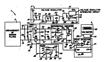
numeral 1, comprises an arrangement 2 of sensor plates
and an electronic circuit 3 including (a) a va~tage
regulator 14, (b) a ti~er 37, (c) a differential
amplifier 49, (d) a peak detector 61, and (e) a
voltmeter 4.
The first arrangement 2 of sensor plates,
as shown in Figure 2, comprises an electrically
conductive central plate 4 and four electrically
conductive side plates 5-8. The five plates 4-8 c~n
be cc,planar (see central plate 4 and side plate 7'
(dashed lines) in ~igure 4). In the illustrated
examp.le, the central plate 4 is square while the side
plates S-8 are elongated and xectanyular. Each side
15 plate:5, 6, 7 or 8 has the same length as the adjacent ~ :
edge æuch as 9 of the central plate ~, it is parallel .
to this edge and is spaced apart therefrom by a :~
distance 10. :~ :-
..
The adjacent ends of each pair of
: successive side plates 5-8 are electrically connected
together through a conductor such as 11 whereby the
side plates 5-8 define an-electrical loop surTounding
the central~sensor plate 4. This central~plate 4 is
25-; electrically connected to the :electronic circuit 3
:: (Figure l) through an electric wire 12~whilè the loop
J~ defined by the interconnected side plates 508 is
connected to this electronic`circuit 3 through another
electric wire 13
:
The arrangement 2 of sensor plates will
be described in further detail in the following
description.
:
W093/0~03 PCT/CA91/~270
~ ..
Referring ~ack to Figure 1, the voltage
regulator 14 comprises a voltage regulator integ ated
circuit 15 supplied with a direct current (DC) supply
voltage Vcc. The integrated circuit 15 produces on
its output 16 a regulated reference DC voltage having
an amplitude which is function of the resistance value
of a potentiometer 18 forming a voltage divider with
a resistor 17. This resistor 17 is connected between
the output 16 a~d another pin 73 of the integrated
circuit 15, and the potentiometer 18 is interposed
between the pin 73 and the ground 19 of the electronic
circuit 3. A capacitor 20, connected between the
output 16 and the ground 19, stabilizes the output
reference DC voltage. The operation of voltage
regulator integrated circuits such as 15 are well
known in the art and accordingly will not be fully
described in the present specification. For example,
the integrated circuit 15 can be constituted by the
voltage regulator (catalogue number TL783C)
commercialized by the company Texas Instruments.
. The voltage regulator 14 also.comprises
an;NPN transistor.21. The transistor 21 has its
collector supplied by the supply DC ~oltage Vcc and
2D~;its~emitter .connected to (a) the positive: supply
terminals of buffers 27 and 28~,-(b~. the input of the
buffer 27 through a resistor 22, (c) the input of the
buffer 28 through a resistor 32, (d) the central plate
4 (Figure 2) through the resistor 22 and the electric
wire 12, and (e) the side plates 5-8 (Figure 2
through the resistor 32 and the wire 13. The base
transistor 21 is connected to the output 16 of the
integrated circuit 15 through a Zener diode 23, having
.
W093/0~03 PCT/CA91/~270
13 2~ 0~
its cathode connected to the base of transistor 21 and
its anode connected to the output 16. A resi~tor 24
is connected in parallel with a capacitor 25 between
the collector and the base of the transi~tor 21.
The regulator 1~ further comprises a PNP
transistor 26 having its collector grounded, its
emitter connected to the negative supply terminals of
the buffers 27 and 28, and its base connected to the
o output 16 of the int~grated circuit 15 through a Zener
diode 29, having its cathode connected to the output
16 and its anode connected to the base of transistor
26. A resistor 30 is connected in parallel with a
capaci.tor 31 between the collector and the base of the
transistor 26.
; :~
~. The electronic circuit 3 further comprises
~a diode 33 having its anode connected to the central
plate 4 through the wire 12, and another diode 34
having its anode connected to the side plates 5-8
through the wire 13. The cathodes of these two diodes
.33.and 34 are connected to the collector of an NPN
transistor. 35. This transistor 35 has its emitter
.~ .grounded and its~base connected to the output 36 of
25~- the timer.37.~
; ~ ~ . : In the embodiment of Figure 1, the timer
37~ comprises a pair of serially interconnected
:~ -inverters 38 and 39, a capacitor 40 interposed between
::30 the input of the inverter 38 and the ground 19, a
resistor 41 interconnecting the input of the inverter
38 and the junction 44 between the output of the
inverter 38 and the input of the inverter 39. As can
W093/0~03 PCT/CA91/~270
be seen, the output of the inverter 3g constitutes the
output 36 of the timer 37. A resistor 43 is connected
in series with a diode 42 between the junction 44 and
the input of the inverter 3~, with the anode of the
diode 42 connected to the input of the inverter 38 and
the cathode of this diode connected to the adjacent
terminal.of the resistor 43.
A first voltage divider is formed ~y
resistors 45 and 46 connected in series between the
outpul: of the buffer 27 and the ground 19 while a
second voltage divider is formed by resistors 47 and
48 serially interconnected between the output of the
buffer 28 and the ground 19.
The differential amplifier 49 has a high
input impedance and includes a first operational
amplifier 50 with a non-inverting input connected to
. the junction between the resistors 45 and 46, and with
an inverting input connected to the inverting input of
another operational amplifier 51 through a resistor
52. The non-inverting input of the operational
. amplifierj51 is connected to the junction between the
resistors 47 and 48. ~ A resistor 54 is connected
between the output and the inverting input of the
operational amplifier S0 while another resistor 53 is
interposed between the output of the amplifier 50 and
the inverting :input of a third operational amplifier
~ :~55. The differintial amplifier 49 further comprises
.a resistor 57 interposed between the output and the
inverting input of the operational amplifier 51 and a
resistor 56 interconnects the output of the amplifier ~ :
51 and the non-inverting input of the third
W093/0~03 ~ PCT/CA91/00270
.,
operational amplifier 55. A re istor 58 interconnects
the output and the inverting input of the operat~onal
amplifier 55. Finally, a resistor 59 is connected
between the ground l9 and the non-inverting input of
the amplifier 55. As shown in Figure 1, the output of
the operational amplifier 55 constitutes the output 60
of the differential amplifier 49.
In the differential amplifier 49, the
resistors 53, 54, 56, 57, 58 and 59 are semi-precision
xesistors of same resistance, the gain of . the
differential amplifier 49 being adjusted by the
resistance value of the resistor 52. The resistor 52
can be formed by a potentiometer to make ~he gain of
differential amplifier 49 adjustable.
The peak detector 61 includes an
operational ampli~ier 62 connected in a voltage-
comparator configuration~ This amplifier 62 has a
non-inverting input connected to the output 60 of the
differential amplifier ~9 through a resistor 63, and
an output connected to the input 68 of the voltmeter
4 through a diode 65 having its anode connected to the
output~of~.the a~plifier 62 and its cathode connected
. 25 to the ~oltmeter input 68. The:inverting input of the~
operational amplifier 62 is connected through a
resistor 64 to the cathode of the diode 65 and to the
collector of an NPN transistor 66 having its emitter
grounded and its base conn~cted to the output 36 of
the timer 37. A capacitor 67 is interposed between
the cathode of the diode 65 and the ground 19.
Accordingly, the capacitor 67 is interposed between
the collector and the emitter of the transistor 66.
j W093/0~03 PCT/CA91/~270
,
2 1 ~ 16
.
'~
As can be seen in Figure 1, the v~ltmeter
4 is connected to the ground 19 of the electronic
, circuit 3 and includes an asæembly 69 of seven-segment
display units. The voltmeter 4 can be replaced by :
5 numerous other devices such as light-e~itt~ng diodes, ;~
bar graphs, sound frequency generators, analog-to~
digital converters, etc. which are also capable of ~ ~:
signalling the level of the voltage peak detected by
the detector 61. . -:
, "~
The structure of the sensing device 1
having been described in detail in the foregoing
description with reference to Figures 1 and 2, its :
operation will now be explained.
_. . .
In operation, the arrange~ent 2 of sensor ~
plates i5 firæt applied to a surface of a structure to .~ :
be investigated. The potentiometer 18 (Figure 1) is :::
then operated to adjust the ratio of the voltage ~;
divider 17-18 and thereby select th~ level of the
reference DC voltage on the output 16. This
~adJustment enabies selection of the level of the
operating voltage of the sensing device 1, taking into
~ consideration the particular application and the level
of sensitivity requiredO
~ The reference DC voltage on the output 16
of the~integrated circuit 15 is supplied to the base
~. of the transistor 21 through the Zener diode 23 and
esta~lishes a biasing voltage on the base of the
transistor 26 through the Zener diode 29~ This
reference voltage accordingly controls the transistors
21 and 26 to determine the level of the operating
- :
:
W093/0~03 PCT/CA9l/~270
17
voltage at the emitter of the transistor 21 (point :~
74). It also adju~ts in function of the opera-ting
voltage at point 74 the amplitude of the DC voltage
between points 74 and 75 (between the emitters o~ the
transistors 21 and 26), supplying the buffers 27 and
28. .
. ~ ...
As can be appreciated by one skilled in
the art, the timer 37 is of conventional structure,
and detailed description of its operation is believed
unnecessary. It produces on its output 36 a periodic
square wave. During each period, this square wave
comprises a low level signal portion applied to the
base of transistor 35 to switch it off. The duration
of the low level signal portion is determined by the
time constant RC of the resistor 41 and capacitor 40.
The DC voltage at point 74 then charges the central
plate 4 through the resistor 22 and the electric wire
12, and the side plates 5-~ through the resistor 32
and the wire 13.
The resistance values of the resistors 22
and 32 are æelected to charge the side plates 5-8 at
a slightly higher~ rate.than the central plate 4.
During the charging of the sensor plates: of the
. arrangement-2, the voltage on the interconnected side
plates 5-8 is slightly higher than the voltage on the
central plate 4. Figure S shows the evolution of the
- voltages.^.on the side plates 5-8 and on the central
plate 4 as the sensor plates charge.
The voltage difference 76 (Figure 5) is
affected by the permittivity of the investigated
s
W093/0~03 PCTJCA91/~270
,, ~ . .
~ 18
2 ~
.
surface and/or sub-surface stru,cture to electric field
itself affected by at least one characteristic of~that
structure, such as the density, composition, internal
configuration, etc. Indeed, as the different plates
4-8 charge, the electric charge on the side plates 5-8
will produce an electric field which oppose to that
produced by the electric charge on the central plate
4. This will reduce the charging rate o the central
plate in function of the permittivity of the
invest:igated structure in which the electric field
propagate, which permittivity is itself related to at
least one of the above mentioned structural
~harac:teristics. This will al~o increase the
amplit:ude of the voltage difference 76 in relation to
th,e reduction of the charging rate of the central
plate 4. As the voltage difference 76 is affected by
the charging rate of the central plate 4 itself
affected by the permittivity to electric field of the
structure under investigation, this voltage difference
is function of this permittivity and therefore of the
said at least one structural characteristic. This
will be further elaborated hereinafter.
The resistance of the resistors 22 and 32
- can be adjusted in factory at given values. They can
also be ,constituted by potentiometers to make them
adjustable. A wide range of adjustments of ~ e
charging rates of the central and side plates and of
~ the operating voltage are possible to take into
consideration the dimensions and configuration of the
sensor plates, the particular application, etc.
, . . , . . , ., ,, .. , .. ....... , , .. , . . ,, . ., . , , .,; . ~
;
: W093/0~03 PCT/CA9l/00270
. . .
19 ~ 3~ `
J
At the end of each period, the square wave
on the output 36 of the timer 37 comprises a high
level ~ignal portion applied to the base of the
¦ transistor 35 to switch it on and discharge to the
ground 19 the sensor plates 4-8 through the diodes 33
and 34 and the junction collector-emitter of the
transistor 35. The diode 42 and the resistor 43 of
the timer 37 cau~es a very fast discharge of the
capacitor 40 during which the output signal of the
timer .37 is high and switches the transistor 35 on.
In the preferred embodiment, the high level signal
portion of each wave period has a duration of 0.2
msec.
As the central 4 and side S-8 plates
charge, the voltage on the central plate 4 is applied
to the non-inverting input of the operational
amplifier 50 through the wire 12, the voltage-follower
buffer 27, and the voltage divider 45-46. Regarding
the voltage on the side plates 5-8, it is applied to
the non-inverting input of the operational amplifier
: 51 through the electric wire 13~ the voltage-follower
;~ buffer 28, and~the~oltage divider 47-~8. Obviously,
the:,buffers..27.and 28 prevent the charging circuit
25~ .14;22;32,12;13 from being.loaded by the~ electronie
circuit 3 of.the sensing device 1.
,..The voltage~ dividers 45;46 and 47;48
~ enable high voltage operation of the sensor plate
30~ arrangement 2. Indeed, these dividers 45;46 and 47;48
reduces the amplitude of such a high voltage to a
level acceptable ~y the differential amplifier 49,
when high voltage operation of the sensing device 1 is
.W~93/0~03 PCT/CA91/~270
2 ~ 1 20
;, ~
-: '
.~selected through the potentiometer 18. Of course, the
resistance values of the resistors 45-48 are selëcted
or are adjustable to supply the operational amplifiers
50 and ~1 with voltages of acceptable levels for all
i5 the amplitudes of operating voltage that can be
supplied by the voltage regulator 14 at point 74 and :
selected through adjustment of the potentiometer 18.
The differential amplifier 49, of which ;
the g,ain is selected by the resistance value of the
resisl:or 52, amplifies the difference between the
voltaS~es applied to the non-inverting inputs of the
operal:ional amplifiers 50 and 51. Accordingly, the
differential amplifier 49 produces on its output 60 an
amplified voltage difference which is representative
of the amplitude of the voltage difference 76 (see
Figure 5) as the central and side sensor plates
charge. .
The amplified voltage difference at the
output 60 of the differential amplifier 49 is applied
: ~ to the peak detector 61. As during charging of the ~ .
. sensor plates 4-8 the signal on the output 36 of the
~-timer~3?~:is low, the junction collector-emitter of the
~25 ~ transistor 66 is non. conductive. Accordingly, the
: operational amplifier 62, connected~in à voltage~
comparator configuration, charges the capacitor 67
through the diode 65 to the voltage amplitude received
on its non-inverting input. As the transistor 66 is . ~ ~
30 switched off by the low level siqnal portion on the ~ -
output 36 of the timer 37 and as the diode 65 is
interposed between the capacitor 67 and the output of
the amplifier 62, one can appreciate that the voltage
,W093/03403 PCT/CA91/00270
s
across the capacitor 67 is representative of the ~ :
highest amplitude of the voltage having appeared-on
the output 60 and accordingly the highest voltage
difference 76 having appeared between the voltages on
5 the central plate 4 and on the side plates 5-8 during ~ ~: the corresponding period ~f the square wave on the
output 36 of the timer 37. - -
.
The voltage across the capacitor 67 is
applied to the input 68 of the vol~meter 4 and its
amplitude is indicated on the display 69. One can
apprec:iate that the displayed voltage amplitude, which
is representative of the hi~hest voltage di~ference 76
as discussed hereinabove, provides the operator with
indications about the characteristics of the structure
under investigation.
.
At the end of each period of the square
wave on the output 36 of the timer 37, the high level
signal portion will switch the transistor 66 on to
discharge the capacitor 67 and thereby reset the peak
detector 61 in view of the next measurement. The
capacitor 67 and the sensor plates of the arrangement
2 are therefore discharged simultaneously to reset the
25i.~ sensing device 1 which is then ready to carry sut
another sensor plate charging operation in view of
performing another measurement.
The arrangement of sensor pIates 2
illustrated in Figure 2 comprises a square central
plate 4. This is not compulsory but selecting the
central sensor plate 4 square will improve the
precision of the device 1 in locating floor joists or
::
W093~0~03 PCT/CA91/00270
-t
. 22
~,
electrically conductive ~ixing nails and/or screws
driven at the sub-floor level in a wood-board finish
floor. ~--
5The dimensions of the central plate 4 may
vary considerably according to the characteristic to
be detected in the structure under investigation. ~ :
Experiments were conducted (a) with a central plate 4
as narrow as s mm and with an operating voltage of 12
volts to measure changes in density at the surface of
wood boards, and (b) with a central plate 4 as wide as
20 cm and with an operating voltage 80 volts to lccate
joists in floors made of heavy wood pieces or made
thicker as a result of resurfacing on top of an
existing floor. These experi~ents gave good results
and demonstrated that the dimensions of the central
plate 4 may widely vary in accordance with the
intended application.
,
20When the embodiment of Figure 2 is used ~
: to precisely locate floor joists and/or sub-floor ~ :
nails and/or screws when they~ are situated in the
center of the. central plate 4, the latter plate is
: advantageously. square with edges 120 mm long, the
25.:~rectangular side plates~5-8 are 120 mm long and 20 mm ~:
wide,~ and- the~:operating.:voltage is 40 volt. This
embodiment is capable of locating joists in a floor :.
made of~20 mm thick wood board sub-flooring covered by
~: 20 mm thick~by 60 mm wide hardwood floor board finish.
.Sensor:plates 4-8 of larger dimensions can however be
used with adequate voltage, when required by the
intended application. ~he thickness of the sensor
plates 4-8 is not a critical factor sinceJ as well
,.
:: .
:
WOg3/0~03 r PCT/CA91/~270
23 . ~ :
known in the art, the electric charge concentrates at
the sur~ace of a conduckor; in practical te~ms,
howe~er, sensor plates 4-8 as thin as 0.1 mm will
properly conduct the charge while minimizing the :
5 losses of electric field through the edges of the :
sensor plates.
In the sensor plate arrangement 2 of
Figure 2, the distance 10 between one edge of the
central plate 4 and the adjacent edge of the
corresponding side plate 5, 6, 7 or ~ is either
permanently ~et or adjustable through a suitable
mechanism (not shown). Experiments were conducted
with distances 10 varying from 2 ~m for surface ~;
density measurement, to 30 mm for locating deep 3~ists
of a wood floor. A larger distance 10 minimizes the
sensitivity of the sensing device 1 ~o the structure
clo~e to the top surface of the floor to which one
face of the arrangement 2 is applied. However, the
distance 10 ~ust not overstep a practical limit for
given dimensions of the central plate 4 and a~given
operating voltage level. Such li~its may be extended
by orienting the side plates 5-8 at an angle 70 (see
Figure 43~.with respect to the -plane of the central
25 ~: plate 4. While the dis~ance lO de~iates thé electric
field,~ as evidenced by the loss of sensitivity to
structure closer to-the surface, a set or adjustable
angle 70 concentrates or focuses the remai~ing ~:
:~ electric field emanating from the central plate 4
deeper in the wood floor structure: this is evidenced
by the possibility of precisely locating target ~ :
elements such as the nails and/of screws fixing the
sub-floor to the joists. In the embodiment of the
::
.
W093/0~03 PCT/CA91/~270
,. ~
~ 24
`:
sensor plate arrangement 2 illustrated in Figures 2
and 4, the distance 10 can be set at 25 mm and-the :~:`
angle 70 is set at 20. These values are adequate to ~ `
locate the joists and sub-floor nails and/or screws in
5 the above-described wood-board finish floor. . :~
,:, .
In the arrangement 2 of sensor plates
illustrated in Figure 3, the electric conductor 11
interconnecting the adjacent ends of the side plates
5 a~d 6, and the electric conductor 11 interconnecting
the adjacent ends of the side plates 6 and 7 are
replaced by electric switches 71 and 72, respectively,
to enable selective connection of the side plates 5-8
to ~orm a loop as shown in Figure 2, or in series as
required in certain applications. It will be readily
understood from the foregoing description that the
.¢onfiguration of the arrangement 2 of sensor plates
should be adjusted in function of better focusing the
electric field in the area of interest, where are
located for example target elements such as the joists
or beams o~ a wood floor, electrically conductive
elements such as nails and/or~ screws in delimited
floor ~areas, for exa~ple- over joists or between
~ oists, aæ desired. .Although the arrangement 2 of
; sensor plates æhown in Figure 3 can be switched from
. one configuration to .the othèx, the distance lo
between each edge of the central plate 4 and the
. adjacent edge of the coxresponding side plate 5, 6, 7
. or 8, and the angle 70 defined by each side plate 5-~
with the plane of the central plate 4, can still be
set or adjusted according to the intended application.
.
W093/0~03 PCT/CA91J~270
,-. :
'2 ~
When the switches 71 and 72 are open, the
downward ~ensitivity of the ~ensing device 1 is nearly
doubled, but preci~e location of small conductive
target elements is improved when the switches 71 and
72 are closed. The switches 71 and 72 therefore
permit detailed analysis of the structure of a wood- :
board finish floor, including precise location of
structural and fixing elements, pipes, wires in any
state of loading or shielding, expansion tanks and any
other elements that should be exactly localized prior
to repairing or for any other purpose. .
Where high precision location of
conductive ~lements und@r a surface is not required,
15 side plate 6 can be removed and side plate 8 replaced :
by a conductor interconnecting the side plates 5 and
7. .However, the adjustable features 10 and 70 are
.~tained. . This configuration of the arrangement 2
rovides for additional flexibility in the geo~etry of
the central plate 4 and a wider range of downward
sensitivity in locating embedded target elements. As :~- indicated in the foregoing description, a central
; plate 4 as narrow:as.5 mm with a distance 10 of 2 mm
:~ will indicate :small ~variations in the density of a
:~:25~ sur`face~of wood (structure under investigation) or of
;~ other~surfaces :made of si~ilar material ctructure. : ~.:
.Larger central plate 4, distance 10 and: operating
voltage~.level will.~enable detection of variations of .
.. density in larger pieces of material.(structure under
30 : investigation~ attr~.~utable to natural variations in -~
fibrous structure, faults, decay, etc. that must be ~.
identified to control quality and classify materials, :~
- . -
.:
W093/0~03 PCT/CA91/~270
, ..
$ 26
, . 'and to assess the structural soundness of elements of
building structures. -~
Extensive experimentation with thesensing
S device 1 indicates that the central plate 4 a~d the
side plates 5-8, in the arrangement 2 o~ Figure 2, are
repeatedly charged with opposing electric charges in
a moving electrostatic condition; as distance 10 and
angle 70, as well as the dimensions and the geometry
of the sensor plates 4-~ vary, the electric field
generated by the side plates 5-8, more or less
circumscribes the electric field generated by the
central plate 4, thus forcing all or most of the
electric field vectors produced by the central plate
4 downwardly into the wood structure, where the local
permittivity to the electric field restricts in
similar proportion dispersion of the electric field
produced by the central plate 4, and th~ charging rate
of that plate 4.
The electronic circuit 3, to which the
arrangement 2 of sensor plates is connected, enables
a broad range of configuration for the sensor plates,
of dimensions and geometry of these sensor plates, of
distances 10, and o~ angles 70, while the voltage
- règulator 14 provides a wide range of electric field
intensity, all of which, acting together, as required,
enable a wide range of applications, of which the
~above-described applications are only non limitative
illustrations. The calibration of the sensing device
may be set in factory, or may be adjustable within a
given range ~through the above mentioned adjustable
eIements) in which the device 1 is readily
WO 93/03403 PCI`/CAgl/00270 ~
!
operational. With the æensing device in accordance
with the present invention, a meaningful readinlg is
obtained each time it is applied locally.
S By applying the device 1 sequentially to
different points of the surface of the stru¢ture under
investigation, local permittivity to electric field is
expressed for each point in terms of the difference
between the charging rate of the side plate 5-8 and
the charging rate of the central plate 4 to provide
the operator with indications of the nature of the
surfac:e and of khe sub-surface. The foregoing
explanations appIy to all the conf~gurations of sensor
plates.
The flexibility in design and easy
operation of the æensing device according to the
present invention provides for operation thereof by a
human operator or machine operator; in the latter
case, a data acquisition and control system would
automatically adjust, for instance, the potentiometer
18, the resistors 22 and 32, the voltage dividers 45-
46 and 47-48, the-resistor 52, etc. a single devi¢e l
or of an array of devices 1, as required by the
25 intended application. ~ -~
Of course, the housing (not shown) of the
sensing device l can be easily adapted to the
application and the operating conditions. In the
above-described preferred embodiment, designed for
investigating wood-board ~inish floor structures, the
arrangement 2 of sensor plates can be mounted on a
thin plate made of a material having a low dielectric
W093/0~03 PCT/CA91/~270
, ~ ':
28
2 1 1 ~
constant such as teflon. This plate can be easily
fitted to the bottom of the housing, which in tur~ is
fitted with a handle structure allowing the operator
to operate and control the device 1 and read the
S display 69 of the voltmeter ~ while standing up a~
about 30 cm away from the sensing device.
Although the present inve~tion has been
described in the foregoing description by means of a
preferred embodiment thereof, it can be modified at
will and applied to various situations, within the
scope of the appended claims without departing from
the ~pirit and nature of the present invention. As an
example, the resistance values of the resistors 22 and
32 (Figure 1) can be adjusted to charge the central
plate 4 and the side plates 5-~ (Figures 2 and 3) at
the same rate when the electric field propagates in a
given ~edium such as air. In the presence of a
structure t~ be investigated, the charging rate of the
central plate 4 will be affected by the local
permittivity and the resulting voltage difference 76
(Figure 5~ will be detected through an amplifier-
multiplier. An amplifier-multiplier should be used as
the voltage,differe~ce 76 will be of lower amplitude
whereby additional sensitivity is required.