Note: Descriptions are shown in the official language in which they were submitted.
:,:',:
WO 93/03491 . P~/US92t06103
i~ 1 4020
C:OLQR 8x~.~h~s8~ZI2~G 8C~h~4J ~~~,'
13I,E:~; ~. KO~ RO8COY~:
Field of the Invention
- The present invention r lates ~enerally to the
f ield of scanning elec:tron micross~opes ~ ~;EM) . More
specifically, the present inventio~ relat~s to a colc:~r
synthesi~ing sc:anrling electrorl microscope conf igured to
produce color images Qf high in~Eormation content by
arranging at least two wide energy bandwidth s~con~ry
detec:~ors around ~ specimen, to de~ect ~lectrons with
tra~ec:tory or po~;itio~al diff~rence~.
Baclc~round o~ the Inven~ic)n
Scanrling electron microscc~c~ are commonly
: u~d for obsenration and analysis of ma~t~r. Scarming
! : ' ' ' ~
electron microscopes have found b~oad application in the
trsnsistor indu ~ry to show voltage distribution in such
desfic~. O~h~r Uses include indu91:rial quali~y eon~rol
2 0 ahd ;~ broad range o~ indus1:rial arld biological research O
A isc~n~2; ng ele tron mic:rcsscope typically
inc:Iudes~ a vacuum chamb~r, :an electron optical syst~m
~: - for generating and ;foeusing an elertron beam (referxed
:: ~ to also as th~ primary elect:ron beam~ a~ a specimen , a
: ~ 25 ~deflection system ~or mc)ving ~he beam acrs: ~s 2 Sp~C~ ell
a predete3:~in~d raster patterrl, a d~tector yst~3m ~or
W093/03491 .,~ ~ ~ ~ PCT/US92/0~103
detecting phenomena from the specimen caused by the
impinging primary electron beam, and a display system.
When the primary electron beam strikes the
specimen, a complex response i5 generated, including
S both short-lived and long-lived phenomena. The short-
lived phenomena include secondary el~ctrons (low
energy), back-scattered electrons (high energy), x-ray
characteris~ics of the specimen, "white x-rays", light
(cathode luminescence), absorbed electrons, transmitted
electrons, and auger process elec~rons (low energy~.
Detectors for each of the above phenom~na are well known
in the art.
Xn a conventional scanning ~lectron
microscope, typically at least one o~ the signals
identi~ied above is detected, amplified and displayed on
a CRT (cathode ray tube). The amplitude of the signal
is used to modulate the intensity of the beam of the
CRT. The beam of the CRT is de~lected in a raster
pattern which COl espon~c~to and is syn~hronized with
the ~ç~nn;ng primary electron beam of the SEM. A black
and white image of the specimen is thereby presented to
the operator of the mi~L~ pe. The i~age thus created
may be set to contain ~hree types of information at each
point on the CRT, two position ~ectors which identify
the location of th~ primary electron beam on the
specimen, and one bri~hLI.css or i~tensity level ~ector
which contains infoxmation~about the specim~n. The
intensity ~evel is usually derived ~rom the secondary
electron emission, which con~ains t~ L aphical (slope)
30 ~ infor~ation. The information thus pr~sented is in a
foxm which is readily acaepted by the h~ n operator who
: can rapidly assimi~ate the information. One or more of
the many signals which are induced by the primary
electron b~am can be di~played in a conv~ntional
scanning electron microscope system at any one time.
W~93/03491 PCT/US92/06103
i11 4~2~
Each of the various respon~es of the specimen
to the primary ~lectron beam includes unique information
about the specimen. For example, the intensity of the
secondary elec~ron emission contains in~ormation about
S the slope of the specim~n sur~ace, with respect to the
primary electron beam. This information can be used to
generate an image o~ the specimen surface. As another
Px~le, the back-scattered (high energy) electron
signal cont ins information about the atomic num~er of
the specimen, and thus can be used ~o provide a profile
having an intensity which is representative of the
chemical makeup rather than the shape of the specimen
under examination. In a conventional scanni~g electron
micro~cope with display, the operator can o~serve any
one or more tha~ one of these images at a time.
Color synthesizers have been ~r ~sed in the
prior art to enhance the ~isplay imag~ of scanni~g
el~ctron micros~opes. For th~ most part, these color
imaging schemes have no~ incr~e1 the information
cont~nt of:the image bu~ haYe been utilized m~rely to
present a more aesthetically pl~asing picture.
Color pictuFes have been produced
photographically~by means o~ multiple expos~res of film
through appropria~ly colore~ filter one prior system
utilizes~three~separate x rays, each representative of 2
different element, which are us~d to modulate the thr~e
: : el~ctron guns of a color kinescope. That is, each x-ray
detector is:a sociat~d~wi~h a diff~ren~ color and these
ele~ents are then displayed concurrently and in color.
~ 30 The resultant ima~e de~ines the distribution of the
: e}em~nts in the specimen since each one is represented
by a different color.
In addition, colored ima~es are constructed in
which differen~ regions of the image are colored in
3S accordance with a color coding scheme, in such a fashion
~093/03q91 PCT/U.592/06103
) 2 0
that variations in a physical variable are represented
by dif fer~nt colors in the image . While such colored
images convey information in a fashion which can be
readily assimilated, the information content i~s
generally no greater than would be c:onv~yed had the
colors not been used and the image simply coded
monochromatically such as by dif~erent shading patterns~
This is ~n contrast to the images normally perceiY~d by
the eye where, because of the added mixed light
impressions psrceived, a variety of lighting effects can
be differentiated, which impressions can hardly be
adequately represented monochromatically~ This arises
because a colored image as percei~ed by the eye can be
con~idered as being made up of three simultaneously
perceived images, each o~ a separate primary color, and
the eye is capable of differentiating r~gions in the
image as to which of the relative proportions of the
three primary colors vary~
U.S~ Patent Nos. 3,628,014, 4,041,311 and
4,560,872 p~o~ t~hniques which generate color images
from the information available in a scanning electron
microscop~ and display the images on a color CRT~ The
îmages are continuous in hué and co~er the entire ~olor
range. Such te~h~iques~ of course, ge~erate color
images in real time as distin~ich~ from photographic
~imag~s. However, these t~h~iques are not useful for
producing color images at the low voltages typically
..
used during; examination of biologicai specimens.
~oreov~r~: the images produced, al~hol~h satisfactory, do
30 ~ not provide a :subs~antial amount o~ information a~out
the specimen. ~
Summary of the I~ven~ion
., ,
~ The present invention is directed to a color
synthesizing scanning electron microscope which produces
W0~3/0349~ .~. P~T~US92/06103
o2O
color images of high information content~ which are more
easily interpr~ted and graphically presented than images
obtained by prior systems~ In a preferr~d embodiment,
the color s~nthesizing scanning electron microscope,
having a scAnning primary beam of electrons directed
toward a sp~cimen, cumprises at l~a~t two wide energy
bandwidth secondary d~tectors arranged around the
specimen at predetermined varia~le angl ~s, ~or receiving
electron emission from the specimen subsequent to
incid~nce of the scanning primary electron beam. The
secondary detectors detect electrons with t~ajectory or
positional differences and convert the differences to
sign~ls for synthesizing color. Means for ~ixing such
signa~s generate signals representatiYe of different
colors.
In a further aspect of the invention, the
angles of the detectors vary ~okh laterally around the
specimen and vertically. ~he variation in the vertical
angle of the det~ctor i5 a factor in deter~in;n~ the
proportion of secondary ~o other elc~L~,.s that are
detected.
In another aspect of the in~ntion a
: differential amplifier generates additional signals for
repre~enting a di~ference between any two input signals
from the secondary detectors.
Brief Descri~tion of th~ ~rawi~as
A preferred embodiment of the pr~sent
invention is illustrated in and by the following
drawings in which like reference numerals indicate like
parts and in ~hieh~
Figure 1 i~ a schematic repr~sent~tlon of a
color synthesizing ~ g ~lectron microscope (SEM~ in
accordance with a preferred embodiment of the pr~sent
inYention;
WO93/03491 ~ 4 ~ ~ ~ PCT/US~2/06103
Figure lA is a schematic represen~ation of a
wide energy bandwidth secondary detectar showing the
manner in which the angle at which it is oriented can be
varied vertically;
Figure lB is a schematic representation of the
wide energy bandwidth secondary detector showing the
manner in which the angle at which it is o~i~nted can be
varied laterally;
Figure 2 is a block diagram of the ~olor video
processor of the color synthesizing SEM;
Figure 3 is a schematic representation of an
exemplary input ampli~ier of the color Yideo processor;
Figur~ 4 is a schematic representation of an
exemplary differential amplifi~r of the color video
processor;
Figure 5 is a schematic representation Qf a
color mixer of the color video procQssor;
Fiyure 6 i~ a schematic representation of a
RGB (Red, Green and Blue) ampli~ier of the color video
pro~es~r; and
Figure 7 is a schematic for the circuitry
r~sponsible for providing the ~ync nd blanking signals.
Detailed Descri~tion of the Preferred Em~odiment
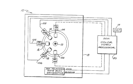
2S Figure 1 illustrates generally a color
synth~sizing ~nni n~ electron ~icroscope 10 in
accordance with a preferre~ ~mbodiment~ of t~e present
invention. The color synthesi2ing SE~ 10 produces color
images of a sp~cimen l~. The color imag~s provide more
information abou~ the speci~en than prior systems, which
: is ~asily interpreted and more graphically presented.
The color synthe~izing SEN 10 is particularly desira~le
for examining specimens at low voltages, for e~Amrle~
when the primary electron beam voltage is 5kV
W093/03491 PCT/US92iO~l03
.... - ' '7Jl,l4020
(kilovolts) and under. Biological and uncoa~ed
specim~ns are typically ~Y~ined at low voltag~s.
In accordance with a preferred embodiment, the
color synthesizing SEM comprises a scanning electron
microscope (SEM) 13, of conventional design. Following
w~ll known techniques o~ the scanning electron
microscope 13, the surface of the specimen 12 is
bombarded with the primary beam of electrons. The
specimen 12 emits secondary electrons that are generated
by the action of the primary electron beam~ These
secondary elec~rons are collected and amplified by the
SEM 13. Since the primary electron beam strikes only
one point one ~he specimen 12, the primary electron beam
is scanned over the specimen 12 in a raster pattern to
generat~ pict~res of the spe~imen sur~ace 12 which are
displayed on a CRT 15.
Major elements of the scanning electron
microscope include electromagnetic lensas (not shown)
t~at are used to form the ele~ . probe, the scan coils
(not shown) that-sweep ~he pri~axy electron beam over
the ~pecimen 12, a deteator 14 that collects the
secondary electrons, and a~plifying r~nR ~indicated at
block llO in Figure 2) where the secondary electrons are
a~plified and fed to the CRT 15 for display. A
conventional vacuum di~fusion pump (not hown~ is used
: since a vacuum is~re~uired for operatlon of the primary
electron be~m.~
-:In a preferred embodiment of the present.
invention, the SE~ is configured such that a~ least two
~o and preferably three ~con~ry dekectors 14, 16 ~nd 18,
~: . associated with the:_c~n~ing electron microscope 10 are
: ~ positioned around the spe~i~en 12 to receive electron
emission from the specimen 12 subsequent to incidence of
the scanning primaxy elec~ron beam to produce images of
the specimen surface in color. The images that are
. W093/0349l PCT/US92/06103
, .. . , ,~.
211-4~0
formed are easily interpreted because the surface
topography, including the illuminating and shadowing
effects on the specimen 12 are similar to large objects
as normally perceived by the unaided eye. The-SEM 13 is
connected to ~ SEM color video processcr 200
The detectors 14, 16 and 18 are con~igured in
accordance with conventional techniques, having suitable
electron voltage potentials applied thereto, to attraat
the seconda~y electrons. In the pre~erred embodiment,
conventional wide energy bandwidth secondary detectors
are used, such as Everhart-Thornley secondary detectors
with wid~A~ photomultiplier tubes and elec~ronicsO A
variable bias ranging between 0 to 300V (volts) is used
for the Faraday cage of the detectors 14, 16 and 18 in
order to appropriately distribute the available signal
elect~ons, thus optimizing signal to nois~ ratio for
each detector. AlternatiYely, other wideband secondary
detectors, such as the micro-channel plate type, can be
used. The detectors 14, 16 and 18 are arranged around
the speci~en 12, at a suit~ble angle to dekect elec~rons
with traj~ctory or positional dif~erenc~s.
~s shown in Fiyu~es lA an~ lB, the angles at
which each of the detector~ 14, 16 and 18 is arranged
can va~y both la~erally and vertically. The variation
in the vertical angle of the detectors 14, 16 and 18
determine ~he~proportion:of secondary to o~her electrons
that are de~ected. In the preferred ~ iment, the
c ntral detector 16 is orien~ed upwards, at a suitable
angle from: tbe perpendicular (~s shown in Figure lA) for
3 0 exa~le 3 0 ~:, and the detectors 14 and 18 axe oriented
such~tha~ they~ aim ~irectly a~ th~ sp~c:imen 12 in order
to de~ct ~ore side-scattered electrons.'
~ore than three detec:tor~; ( additional
: detectors ~2 and 24 are shown in Figure 1 in broken
lilles~ with associated input amplifiers, differential
WO93/03491 . . PC~iUSg2/06103
~ 1 4~2~
amplifiers and RGB mixers can be used. The detectors
can be arranged in an arc or a full clrcle to entirely
surround the specimen 12. Each of the detectors can be
turned on or of f, as desired, to experiment with vari~ous
signals for the purpose of image ana}ysis and to adjust
"illumination" ~chiaroscuro) by the electrons for
recarding purposes. A back-scatter detector (either
solid state, scintillator or micro channel plate (MCP)
can also be used to detect back-scattered elec~rons. If
a back-scatter detector is used~ a relatively high
acceler~ting beam ~oltage o~ lOkV or 20kV and above is
desired.
Figure 2 is a block diagram of the color video
processor 20 of the color synthesizing SEM 10 of the
present invention. The co}or video process~r ~0 can be
used in applications other than in secondary electron
~icroscopes to deri~e color signals from three black and
white signals. Chan~els 102, 104 and 106 from each of
th~ wide energy bandwidth ~onA~ry detectors 14, 16 and
;20 18, r~srDctively~ are connected to an input amplifi3r
~: 110. The input amplifier llO~compri~es ~hree separate
input amplifier stages, a first amplifier stage 112
connected to a channel 10~, a second amplifier stage 114
:~ connected to a second ç~n~el 104 and a third amplifier
~ 25 stage:ll6 connected to a~third channel 106. The
: : amplifier stages 112, 114 and 116:buffer and amplify the
c~~~els(102, 104~,and~-106,:1~~ ively, if n~r~C~ary.
. . The ~L~s of the ampli~ier stages llZ'~ 114
and 116 are connected to~a differential amplifier stage
: ~30 150. ~The differential:amplifier~ta~ 150 g~nera~es
additional signals a~ the sutput5 of the amplifiex
stages 112, 114 and~116. The differ~ntial amplifier
stage 150 genera~es signals representative of the
dif~erence between any~wo of the signals at the ou~-puts
of the amplifier stages 112, 114 or 116. This stage is
WO~3~03491 2 1 l 4~ 2 0 PCr/USg2iO6103
particularly useful for producing a third signal in
situations where only two wide energy bandwidth
secondary detectors are used. In situations where more
than two secondary d~tectors are used, any number of
difference signals may be generated by adding a
differenti~l amplifier ~or each desired difference
signal.
The outputs ~xom th~ differential output stage
150, along with the outputs from the amplifier stages
112, 114 and 116, are connected to a color mix~r 200.
The color mixer ~00 mixes those signals and produces
three outputs 202, 204 and ~06, each representative of
the colors red, green and blue, réspectively.
The outputs 20~, 204 ~nd 206 ~rom the color
mixer 200 are connected to an RGB ampli~ier stage 250.
The RGB amplifier stage 250 amplifies each of the red,
gr~en and blue signals at the outputs 202, 204 and 206
from the color mixer 200. The RGB amplifier stage 250
may be adjusted to vary the amount o~ signal going to
~0 ~ach of the ouL~ color ch~n~el~ 252, 254 and 256.
The ou~u~ ~h~nnels 252, 254 and 256 from the
RGB amplifier stage 250 are preferably conneck~d to a
sync and blanking stage 300 which adds the appropriate
video blanking and sync signals, which are in
synchronization with the _c~ primary beam of the
color~synthesizing SE~ 10 of the present invention. The
sync and b}~nking stage 300 produces red, green and blue
ch~nnels 302, 304 and 306, respecti~ely, and a ch~nnel
monitor signal 308. The red, green and ~l~e ch~nnei~
are video ~si~n~l~ and th~ chann~l monitor signal 308 is
a ~T5C: coTaposite vid~o sigllal that enables the op~rator
to monitQr the signal and corresponding image of any of
~nn~l S 112, 114, ~116 or 15~ in blaclc ;lnd whit2,
independent of the color ou~ . This signal may as
well be simultaneously noise redu ::ed, transcoded and
- WO93J03491 PCT/US92/06103
...4~2(0
11
record~d. Alternatively, the output chann~}s 252, 254
and 256 can be conn~cted to a film recorder, A/D
converters, computer or the li~e.
The output channels 302, 304, 306 an~ 308 m~y
be then connected to any suitable video e~uipment ~or
viewing the image produced by the color ~ynthesizing SEM
lO. Optionally, th~ output channels 302, 304, 306 and
308 may be connected to a frame averager 350, of
conventional design known to those skilled ln the art,
for noise reduction. The frame averager 350 produces
red, gre~n, blue, and sync output channels 352, 354, ~56
and 358.
The output channels 3S2, 354, 356 and 358 from
the ~rame averager 350 may be optionally connected to a
vid~o transcoder 400, o~ conventional design Xnvwn to
~hose skilled in the art. The video transcoder 400
produces ~u~site, YjC (S-VHS~, co~ponent or other sync
output ~h~ l S 402, ~04, 406 and 408, respectiv~ly, for
. connection to appropriate video ~quipment.
: Figur~ 3 is a schematic repre ~ntation o~ the
an exemplary input ampli~ier ~tage llO of the color
video proce~sor 20. The se~ondary detector ~hannels
102, 104 and 106 ~re connected to the input amplifier
stages 112, I14 and 11~, resp~ctively, as shown in
: 25 Figure 2. The input amplifier stage~ 112, 114 and 116
-j are substantially identical ~nd are represented by the
. ~ circuit diagram shown in Figur~ 3. The input amplifier
stage 112 has resistors Rl, R2, R3, R4, RS, R~, R7, R~
~ a~d R9, ha~ing exemplary re~istance values of 150n
: (ohms), 7sn, 250n, 250n, 20n, 390Q, 560n, 75~ and 7~,
: : respec~iY~ly. The inpu~ amplifier stage 112 has
- capacitors Cl an~ C2, having ~x~mplary capacitance
values of 10~F (micro~arads) and 3pF (picofarads~,
respectively. The input amplifier stage 112 has an
operational amplifier Ul, ha~ing exemplary part number
~093/03491 P ~/US92/06103
,.. .
'~114Q'~.U
12
621 manufactured by Burr-~rown, and a buffer amplifier
U2 to monitor the channels, ha~lng exemplary part number
2001 manufactured by Elantec.
A three pole, double throw switch Sl.connects
or disconnects the input amplifier 112 from an output
channel 122 which is connected to the differential
amplifier stage 150 (shown in Figure 2). A pole ~26 of
the ~witch 124 is connected to a voltage of preferably
3V. When the switch 124 is in a connected position, as
shown in Figure 3, the po~e 126 is connected to an
indicator lamp 128, indicating that the output of the
amplifi~r stage 11~ is connected to the output channel
122. When the switch 124 is in a disconnected position,
the indicator lamp 128 is disconnected and the output
channel 12~ is also disconnected Prom the input
amplifier stage 112. The ou~,uL of the resistor R9 of
the input amplifier stage 112 is connect~d to a monitor
select switch 310 ~shown in Figure 7).
Figure 4 is a sche~a~ic representation of the
di~ferential anplifi~r 152 of the differen~ial amplifier
: stage 150 and~ exemplary of all th~ dif~er~ntial
amplifiers includ~d within the stage 150. The
differential amplifier 152 has a vaxiable resistor VRl,
: which has an exemplary resistance value o~ lkn and which
is connected to a double pol~, double throw switch S2.
The: varlable resistor VRl adjusts the balance betwe~n
in~uts,l54 and~156 ~also shown in-Figure 2).~ The
~: di~ferential~amplifier 152 has re~istor~ RlO, Rll, R12,
R13, R14, Rl5, R16, R17 a~d R18, having exemplary!
: 30 resistance values of 110~ n, 250n, 250n, 20n, 560n,
~90n, 75n and ~:75sa, respec:tively. Th diff2rential
a~plifier 152 ~has an operational amplifier U3 having
exemplary part number 620 or 621 manufactured by Burr-
Brown and a buffer amplifier U4 having exemplary part
number 2001 manufactured by Elantec. The output of the
W093/0349~ PCT/USg2i~6~3
2:1..1.40~0
13
resistor R18 is connected to the monitor select switch
310 (shown in Figure 7~.
Figure 5 is a schematic representation o~ the
color mixer 200 shown ~or an exemplary configuration of
three secondary det~ctor channels 208, 210 and 212, and
two differential output channels 214 and 216 from the
differential amplifier stage 150. Each channel is
connected to three variable resistors, each indicated at
VR2 and having an exemplary resistance value of 500n.
Each ~ariable resistor VR2 is connected to a resistor
Rl9, R20 and R21, each havlng exemplary rasistance
valu~s of 250n. The r~sistors ~19, R20 and R21 ar~
connected to the red output channel~ 202, the green
output channel 204 and the blue output channel 206,
respectively.
Figure 6 is a schematic representation of the
RGB amplifier 2500 The ~G~ amplifier ~50 has preferably
three amplifi~rs on a chip having an ~Y~rlary part
number LM 1203 manufac~ured by Texas Instruments.
Resistors R22, R23, ~ R24, R25 and R2G, have ex~mplary
resistanc values of 75~, lolcn, lson,~ 390n and 75n,
respectively. The~ RGB amplifier has a variable resistor
VR3 for varyin~ the gain of the red, green and blue
outputs, and ~TR4 for calibrating the gains of each of
2S th~ red, green and ~lue ouiv~ channels 252, 254 and
- 256, having~ Qx~mplary~ resistanc~e values of lOkQ and
. ;.. lOOn, respectively.- The RGB amplifier~has capacitors
C3, C4,: C5, C6~, C7, C8, C9 and ~::10, ha~ring exemplary
capacitance values of lO~F (microf~rads), lO~F, O.l~F,
O.lpF, lO~F, ~ F~; O.l~F and lOO~F, respectiYely. Th~
output channels 252, 254: and 256 from the RGB amplifier
~stage 250 are p~Qferably connected to a sync and
. . blanking s~age 300, as shown in Figure 2~
;~ Figure 7 is a schematic representation o~ the
sync and blanking stage 300. A blanking i~put 302 is
W~93/034gl PCT/US92/06103
.. . .....
~ 4~)2 0 14
connected to an NPN transistor Q1, having an exemplary
part number 2N3904 manufactured by Motorola, and a PNP
transistor Q2 t having an exemplary part number of 2N3906
manufactured ~y Motorola. Resistors R27, R28, ~29, R3
and ~31, having ~Y~lary resistanc~ values of 83kn,
24XS~, 3.6kn, 24kn, and 1.8kn, and diodes Dl, ha~ing
exemplary part number lN914, are connected to the
transistors Ql and Q2.
Transistors Q3 and Q4 are coupled between the
output 252 from the ~B ampli~ier 250 and the red output
302 from the sync and blanking pulse adder 300 (shown in
Fi~ure 2) and have exemplary part numbers o~ 2N4239 and
2N5639, respectively. ~esistors R32, X42, R43, R44~ R45
an~ R46, having exemplary resistance values of 39kn,
75n, 290n, lOOn, 18kn and 470n, respectiYely, and
capacitoxs C11 and C13~ each ha~ing an exemplary
capacitance value of 100~, are connected to the
transistor~ Q3 and Q4. Variable resistor VR5~ having an
exemplary resistance value of 50kn, adjusts the
brightness of the red signal. Diode ~1 is connected
between the transistors Q3 and Q4.
The circuit connected between the output 254
frcm the RGB amplifier 250 and ~he green output 30~, the
circuit connect~ between the output ~56 from the R~B
amplifier 250 and the blue ouL~L 306, ~nd the circuit
connected between~the moni~or select switch 310 and a
transistor Q5 are all confi~ured in an identical ma~ner
with the circui~ between ~he o~Ly~ 25~ from the RGB
amplifier 250 and the red ou~u~ 302. Each cirru~t is
shown in Figure 7 within broken lines.
The transistor Q5 is a PNP transistor having
an exemplary part number of 2~3906 manufactured by
Motorola. Resistors ~37, R38, ~39 and variable r~sistor
VR7, having exemplary resistance values of 7.5~, 27k~,
WO 93/03491 P~iUS~2/061~3
. .. ..
1 4~
lOOr2 and 5kn, are connected between the transistor Q5
and a sync input 312.
Although the invention has been described in
terms of a preferred embodiment thereof, other-
embodiments that will now be apparent to those of
ordinary skill in the art are also within the scope of
the inventior~ ccordingly, the scope of the invention
is intended to be defined only by reference to the
appended claims.
,
'