Language selection

Search

Patent 2114363 Summary

Third-party information liability

Some of the information on this Web page has been provided by external sources. The Government of Canada is not responsible for the accuracy, reliability or currency of the information supplied by external sources. Users wishing to rely upon this information should consult directly with the source of the information. Content provided by external sources is not subject to official languages, privacy and accessibility requirements.

Claims and Abstract availability

Any discrepancies in the text and image of the Claims and Abstract are due to differing posting times. Text of the Claims and Abstract are posted:

  • At the time the application is open to public inspection;
  • At the time of issue of the patent (grant).
(12) Patent Application: (11) CA 2114363
(54) English Title: TEMPERATURE-STABILIZED OSCILLATOR CIRCUIT HAVING HEATING ELEMENTS THAT CAN BE EXTERNALLY INFLUENCED
(54) French Title: MONTAGE OSCILLATEUR A TEMPERATURE CONTROLEE DONT LES ELEMENTS CHAUFFANTS PEUVENT ETRE OU NON MIS SOUS TENSION
Status: Dead
Bibliographic Data
(51) International Patent Classification (IPC):
  • H03B 1/00 (2006.01)
  • H03L 1/02 (2006.01)
  • H03L 1/04 (2006.01)
  • H03L 7/08 (2006.01)
(72) Inventors :
  • ZWACK, EDUARD (Germany)
(73) Owners :
  • SIEMENS AKTIENGESELLSCHAFT (Germany)
(71) Applicants :
(74) Agent: FETHERSTONHAUGH & CO.
(74) Associate agent:
(45) Issued:
(22) Filed Date: 1994-01-27
(41) Open to Public Inspection: 1994-07-30
Availability of licence: N/A
(25) Language of filing: English

Patent Cooperation Treaty (PCT): No

(30) Application Priority Data:
Application No. Country/Territory Date
P 43 02 529.3 Germany 1993-01-29

Abstracts

English Abstract


ABSTRACT OF THE DISCLOSURE
In an oscillator circuit (VCOS) having at least one heating
element (HE) that keeps the temperature constant, the clock signals
(ts) that are formed are conducted via an output connection (AV) to
an output (TA) of the oscillator circuit (VCOS). An impedance
evaluation unit (WAE) is inserted into this output connection (AV)
and is fashioned such that a change is recognized of an impedance
or of a resistor (R4, R5) connected to the output (TA) and the
heating element (HE) is activated or deactivated in response to
changes in the impedance.


Claims

Note: Claims are shown in the official language in which they were submitted.


WHAT IS CLAIMED IS:
1. An oscillator circuit having at least one heating element for
keeping the temperature of the oscillator circuit substantially
constant, comprising:
oscillator means for forming oscillation signals;
oscillator output circuit connecting said oscillator means to
an oscillator output of the oscillator circuit, said oscillator
output circuit conveying said oscillation signals from said
oscillator means to said oscillator output; and
an impedance evaluation means connected to said at least one
heating element for detecting a change in an impedance means
connected to said oscillator circuit, said at least one heating
element being activated and deactivated as a function of the change
in said impedance means.

2. The oscillator circuit according to claim 1, wherein said
oscillator circuit further comprises: a precision oscillator that
provides oscillating measured signals; a measured output circuit
connecting said precision oscillator to a measured output of the
oscillator circuit; said impedance evaluation means being arranged
in said measured output circuit and said impedance means being
connected to said measured output.

3. The oscillator circuit according to claim 2, wherein said at
least one heating element is a heating resistor, and wherein said
at least one heating element is switched between a heating mode and
a quiescent mode by a serially connected switching transistor.


4. The oscillator circuit according to claim 2, wherein said
impedance evaluation means comprises: a first resistor connected
between said precision oscillator and said measured output; a first
switching transistor having an emitter-base path connected in
parallel to said first resistor and a collector connected to a
second switching transistor in an emitter follower configuration;
switching of the first switching transistor and of the second
switching transistor being effected by a change for one impedance
value to another different impedance value of the impedance means.

5. The oscillator circuit according to claim 2, wherein the
impedance means comprises two series connected resistors and a
switching transistor connected across one of said two serial
connected resistors, whereby switching of said switching transistor
changes the impedance value of said impedance means.

6. The oscillator circuit according to claim 1, wherein said
impedance evaluation means is arranged in said oscillator output
circuit and said impedance means is connected to said oscillator
output.

7. The oscillator circuit according to claim 6, wherein said at
least one heating element is a heating resistor, and wherein said
at least one heating element is switched between a heating mode and
a quiescent mode by a serially connected switching transistor.


8. The oscillator circuit according to claim 6, wherein said
impedance evaluation means comprises: a first resistor connected
between said oscillator means and said oscillator output; a first
switching transistor having an emitter-base path connected in
parallel to said first resistor and a collector connected to a
second switching transistor in an emitter follower configuration;
switching of the first switching transistor and of the second
switching transistor being effected by a change for one impedance
value to another different impedance value of the impedance means.

9. The oscillator circuit according to claim 6, wherein the
impedance means comprises two series connected resistors and a
switching transistor connected across one of said two serial
connected resistors, whereby switching of said switching transistor
changes the impedance value of said impedance means.

10. An oscillator circuit having at least one heating element for
keeping the temperature of the oscillator circuit substantially
constant, comprising:
oscillator means for forming oscillation signals;
oscillator output circuit connecting said oscillator means to
an oscillator output of the oscillator circuit, said oscillator
output circuit conveying said oscillation signals from said
oscillator means to said oscillator output;
a precision oscillator that provides oscillation measured
signals;
a measured output circuit connecting said precision oscillator
to a measured output of the oscillator circuit; and

11


an impedance evaluation means connected to said at least one
heating element and arranged in said measured output circuit for
detecting a change in an impedance means connected to said measured
output of the oscillator circuit, said at least one heating element
being activated and deactivated as a function of the change in said
impedance means.

11. The oscillator circuit according to claim 10, wherein said at
least one heating element is a heating resistor, and wherein said
at least one heating element is switched between a heating mode and
a quiescent mode by a serially connected switching transistor.

12. The oscillator circuit according to claim 10, wherein said
impedance evaluation means comprises: a first resistor connected
between said precision oscillator and said measured output; a first
switching transistor having an emitter-base path connected in
parallel to said first resistor and a collector connected to a
second switching transistor in an emitter follower configuration;
switching of the first switching transistor and of the second
switching transistor being effected by a change for one impedance
value to another different impedance value of the impedance means.

13. The oscillator circuit according to claim 10, wherein the
impedance means comprises two series connected resistors and a
switching transistor connected across one of said two serial
connected resistors, whereby switching of said switching transistor
changes the impedance value of said impedance means.

12


14. An oscillator circuit having at least one heating element for
keeping the temperature of the oscillator circuit substantially
constant, comprising:
oscillator means for forming oscillation signals;
oscillator output circuit connecting said oscillator means to
an oscillator output of the oscillator circuit, said oscillator
output circuit conveying said oscillation signals from said
oscillator means to said oscillator output;
a precision oscillator that provides oscillation measured
signals;
a measured output circuit connecting said precision oscillator
to a measured output of the oscillator circuit;
an impedance evaluation means connected to said at least one
heating element and arranged in said measured output circuit for
detecting a change in an impedance means connected to said measured
output of the oscillator circuit, said at least one heating element
being activated and deactivated as a function of the change in said
impedance means, said impedance evaluation means having a first
resistor connected between said precision oscillator and said
measured output, and having a first switching transistor with an
emitter-base path connected in parallel to said first resistor and
a collector connected to a second switching transistor in an
emitter follower configuration, switching of the first switching
transistor and of the second switching transistor being effected by
a change from one impedance value to another different impedance
value of the impedance means; and
said impedance means having two series connected resistors and
a third switching transistor connected across one of said two
serial connected resistors, whereby switching of said third
switching transistor changes the impedance value of said impedance
means.
13


15. The oscillator circuit according to claim 14, wherein said at
least one heating element is a heating resistor, and wherein said
at least one heating element is switched between a heating mode and
a quiescent mode by the second switching transistor.


14

Description

Note: Descriptions are shown in the official language in which they were submitted.


~J~ ~3~3

BACKGROUND OF THE INVENTION
Telecommunications equipment, particularly communications
equipment, IS equipped with temperature-stabilized oscillator
circuits for the purpose of forming high-precision alternating
signals, particularly clock signals. The oscillator circuits are
mainly realized by voltaye-controlled oscillator circuits that form
part of a phase-locked loop. With the assistance of these phase-
locked loops, the clock signals formed in the communication systems
are controlled synchronously with respect to their phase to a
reference clock siynal supplied to the communications system, for
examplel from a higher-rankiny clock means. The phase-locked loop
is mainly formed by an oscillator circuit and by a means that
further-processes the clock siynals. The control signals for
controlling the heating elements are usually formed in these
further-processing means, for example, a microprocessor system
equipped with appropriate programs, and are communicated to a
separate input of the oscillator circuit for controlling the
heating elements. The measurement of the current temperature in an
oscillator circuit is thereby effected either via a temperature
sensor element, for example a semlconductor temperature sensor, or
by a temperature-measuring oscillator. A temperature-measuring
oscillator is;realized such that optimally large frequency changes
of the formed clock signals are produced for temperature changes.
These temperature sensor signals or measuring oscillator signals
are evaluated in the further-processing means and the current
temperature of the oscillator circuit is calculated. Dependent on
the result of the temperature measurement, the heating element in
the oscillator circuit is subsequently activated via separate
connections or is s~itched off in such a way that the temperature
of the oscillator circuit remains largely constant.


f ~3 L~3g3

SUMMARY OF THE INVENTION
It is an object of the present invention to reduce the outlay
for an external control of the heating elements arranged in the
oscillator circuit.
In general terms the present invention is an oscillator
circuit having at least one heating element that keeps the
temperature constant. The oscillation signals that are formed are
conducted via an output connection to an output of the oscillator
circuit. An impedance evaluation unit is inserted into the output
connection and is fashioned such that a change in an impedance
connected to the output of the oscillator circuit is recognized and
the at least one heating element is activated or deactivated in
response to changes in the impedance.
An important aspect of the oscillator circuit of the present
invention is that an impedance evaluation unit is inserted at the
exiting output connection between the actual oscillator and the
output of the oscillator circuit and is fashioned such that a
variation of an impedance or a resistor connected at the output is
recognized and the heating element or the heating elements are
activated or deactivated. An important advantage of the oscillator
circuit of the present invention is that a separate connection
between a further-processing means and the oscillator circuit can
be foregone for activating or deactivating the heating elements.
Thus, the outlay with respect to plug devices and connecting lines
is substantially reduced.
Given employment of a precision oscillator in an oscillator
circuit, the impedance evaluation unit is especially advantageously
connected to the output connection between preclsion oscillator and
the measured output of the oscillator circuit. The activation or
deactivation of the heating elements is thereby effected by a


3 ~ 3


change of an impedance or of a resistor connected to the measured
output of the oscillator circuit. In this realization, the
temperature of the oscillator circuit as well as the acti~ation or
deactivation of the heating elements can be implemented via a
single measured output of the oscillator circuit:.
In an advantageous development of the oscillator circuit of
the present invention, the heating element or the heating elements
is or are realized by filament resistances, these being driven into
a heating or quiescent condition by a serially connected control
resistor. This represents an especially economical realization of
a heating element including the appertaining control thereof.
The impedance evaluating means is advantageously realized by
a resistor inserted into the output connection as well as by a
switching transistor whose emitter-base path is connected as an
emitter follower to the control input of the control transistor
parallel to the resistor and to the collector thereof. The
switching of the switching transistor is effected by connecting
different impedances or resistances to the output or measured
output of the oscillator circuit. The activation or deactivation
of the heating elements is possible using this extremely low-outlay
realization of an impedance evaluation means by simply varying an
impedance, usually realized with resistors, connected to the output
or measured output of the oscillator circuit.
The impedance that can be connected to the output or measured
output is especially economically realized by two resistors,
whereby one of the two resistors is activated or deactivated by a
further switching transistor for the purpose of modifying the
impedance. The resistor that is inserted into the output
connection, as well as the two resistance forming the impedance are
dimensioned such that, first, the switchiny transistor is switched


3 ~ ~


by activating or deactivating a resistor and, second, that the
further-processing of the clock signals or measured signals
continues to be assured. The further-processiny, for example,
occurs in a processing means of a phase-locked loop, whereby the
impedance existing in the two resistors and the further switching
transistor as well as a control procedure required therefor are
provided in the processing means.
BRIEF DESCRIPTION OF THE DRAWING
The features of the present invention which are believed to be
novel, are set forth with particularity in the appended claims.
The invention, together with further objects and advantages, may
best be understood by reference to the following description taken
in conjunction with the accompanying drawing, and in which:
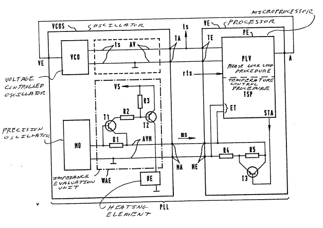
The single Figure is a block diagram of an oscillator circuit
of the present invention.
DESCRIPTION OF THE PREFERRED EMBODIMENT
The single Figure shows a phase-locked loop PLL that is formed
of a voltage-controlled oscillator circuit VCOS and of a processing
means VE. The oscillator circuit VCOS has a clock output TA to
which the clock signals ts, for example, digital clock signals,
formed in a voltage-controlled oscillator VCO are conducted via
output connections AV. The voltage control input VE of the
oscillator circuit VCOS is connected to the output A of the
processing means VE.
It is also assumed for the exemplary embodiment that a
precision oscillator MO is arranged in the oscillator circuit VCOS.
This precision oscillator MO is provided Eor measuring the
temperature of the oscillator circuit VCOS. To this end, the
precision oscillator MO is fashioned such that optimally
substantial frequency changes of the digital measured signals ms


3 ~ 3


occur for temperature changes. This is usually achieved by known
specific temperature-measuring crystals that are not shown. The
measured signals ms formed in this manner proceed via a further
output connection AVM to a measured output MA of the oscillator
circuit VCOS. A resistor Rl is inserted into one of the two lines
of the further output connections AVM. The base-emitter path of a
first NPN switching transistor Tl is connected in parallel to this
resistor R1. The collector of this first switching transistor T1
is connected via a second resistor R2 to the base of a second PNP
control switching transistor T2 in an emitter-follower circuit.
The base of this control switching transistor T2 is connected to
the supply voltage VS of the oscillator circuit VCOS via a third
resistor R3 as well as via its emitter. The collector of the
second switching transistor T2 is connected to the heating element
HE that is preferably realized by appropriate heating resistors or
filament rheostats.
The measured output MA of the oscillator circuit VCOS is
conducted to a measuring input ME of the processing means VE via
appropriate connections. The two inputs of the measuring input ME
are connected both to a processor means PE, preferably a
microprocessor, as well as via two serially connected, follrth and
fifth resistors R4, R5. The collector-emitter path of a third
transistor T3 is connected in parallel to the fifth resistor R5,
whereby the base of this third transistor T3 is connected to a
control output STA of the processor means PE. Further, the clock
signals ts and reference clock`signals rts which, for example, are
supplied from a higher-ranking clock means are supplied to this
processor means PE via a clock signal input TE. The functions that
are relevant to the phase-locked loop such as, for example, phase
comparison, low-pass function and digital-to-analog conversion of


3 ~ 3

the control signals are realized with a PLL procedure PLV
implemented in the processor means PE. The measured siynals ms
incoming at the input ET are evaluated with respect to their
frequency, and the current temperature of the oscillator circuit is
derived therefrom usin~ a further temperature control procedure TSP
implemented in the processor means PE. Corresponding to the
derived result of the temperature measurement, the third control
transistor T3 is switched via the control output STA such that the
fifth resistor R5 is either substantially shorted or is introduced
between the two inputs of the measuring input ME in series with the
fourth resistor R4. As a result thereof, a change in impedance,
i.e. a change in resistance is effected at the measured output MA
of the oscillator circuit VCOS. This impedance change at the
measured output MA of the oscillator circuit VCOS produces
different voltage drops at the first resistor R1. The first,
fourth and fifth resistor R1, R4, R5 are dimensioned such that the
voltage drop at the first resistor R1 causes the first transistor
Tl to be either conductive or non-conductive. This conductivity or
non-conductivity of the first transistor T1 drives the second
transistor T2 either into its non-conductive or conductive
condition. As a result thereof, the heating element HE is either
activated or deactivated.
The first, second and third resistors R1, R2, R3, as well as
the first and second transistors T1, T2 form an impedance
evaluation unit WAE, as shown with broken lines in the Figure.
Given the absence of a precision oscillator MO, for example given
a realization of an oscillator circuit VCOS with a temperature
sensor, the impedance evaluation unit WAE can be introduced into
the output connection AV between the oscillator VCO and the clock
output TA, as shown with broken lines in the single Figure. The


" 2~ 1~3~3


control unit formed by the fourth and fifth resistors R4, R5 and by
the third switching transistor T3 is thereby to he connected to the
clock input TE of the processing means VE. In both versions, the
third and fourth resistors R4, R5 are dimensioned such that a
recognition and evaluation of the incoming measured signals ms or
clock signals ts is possible given inserted and shorted fifth
resistor R5. Due to the insertion of an impedance evaluation means
WAE in the oscillator circuit VCOS and of a control unit in the
processing means VE, a separate connection for controlling the
heating element HE with the processing means VE can be foregone.
The savings in outlay with respect to plugs and connecting lines to
be potentially inserted exceed the slight circuit-oriented outlay.
The invention is not limited to the particular details of the
apparatus depicted and other modifications and applications are
contemplated. Certain other changes may be made in the above
described apparatus without departing from the true spirit and
scope of the invention herein involved. It is intended, therefore,
that the subject matter in the above depiction shall be ~nterpreted
as illustrative and not in a Iimiting sense.


Representative Drawing
A single figure which represents the drawing illustrating the invention.
Administrative Status

For a clearer understanding of the status of the application/patent presented on this page, the site Disclaimer , as well as the definitions for Patent , Administrative Status , Maintenance Fee  and Payment History  should be consulted.

Administrative Status

Title Date
Forecasted Issue Date Unavailable
(22) Filed 1994-01-27
(41) Open to Public Inspection 1994-07-30
Dead Application 2002-01-28

Abandonment History

Abandonment Date Reason Reinstatement Date
2001-01-29 FAILURE TO PAY APPLICATION MAINTENANCE FEE
2001-01-29 FAILURE TO REQUEST EXAMINATION

Payment History

Fee Type Anniversary Year Due Date Amount Paid Paid Date
Application Fee $0.00 1994-01-27
Registration of a document - section 124 $0.00 1994-07-26
Maintenance Fee - Application - New Act 2 1996-01-29 $100.00 1995-12-20
Maintenance Fee - Application - New Act 3 1997-01-27 $100.00 1996-12-19
Maintenance Fee - Application - New Act 4 1998-01-27 $100.00 1997-12-17
Maintenance Fee - Application - New Act 5 1999-01-27 $150.00 1998-12-18
Maintenance Fee - Application - New Act 6 2000-01-27 $150.00 1999-12-17
Owners on Record

Note: Records showing the ownership history in alphabetical order.

Current Owners on Record
SIEMENS AKTIENGESELLSCHAFT
Past Owners on Record
ZWACK, EDUARD
Past Owners that do not appear in the "Owners on Record" listing will appear in other documentation within the application.
Documents

To view selected files, please enter reCAPTCHA code :


To view images, click a link in the Document Description column. To download the documents, select one or more checkboxes in the first column and then click the "Download Selected in PDF format (Zip Archive)" or the "Download Selected as Single PDF" button.

List of published and non-published patent-specific documents on the CPD .

If you have any difficulty accessing content, you can call the Client Service Centre at 1-866-997-1936 or send them an e-mail at CIPO Client Service Centre.


Document
Description 
Date
(yyyy-mm-dd) 
Number of pages   Size of Image (KB) 
Cover Page 1994-07-30 1 76
Abstract 1994-07-30 1 26
Claims 1994-07-30 6 283
Drawings 1994-07-30 1 42
Description 1994-07-30 7 387
Representative Drawing 1998-08-28 1 29
Fees 1996-12-19 1 76