Note: Descriptions are shown in the official language in which they were submitted.
CFO 9751 ~sc~A
- 1 - 2114D~78
l Method of Manufacturing Image-forming Apparatus
And Image-Forming Apparatus
Manufactured by Using the Same
BACXGROUND OF THE lNv~NllON
Field of the Invention
This invention relates to a method of manu- ~ ~'
facturing an image-forming apparatus such as a display ~ ~'
apparatus in which images are formed by irradiation of
electron beams and it also relates to an image-
forming apparatus manufactured by using said method.
Related Background Art '~
::, :
Known electron-emitting elements are currently
classified into two categories. Those that are used
as thermoelectron sources and those used as cold
cathode electron sources. Of these, cold cathode
electron sources are normally groupea as one of -~
several types including the field effect emission
type ~hereinafter referred to as FE type), the metal/
20~ insuLation layer/metal type (hereinafter referred
to as MIM type~ and the surface conduction type.
Some FE type devices are proposed in W. P.
Dyke & W. WO Dolan, "Fieldemission", Advance in -
Electron Physics, 8,89 (1956) and C. A. Spindt,
"Physical properties of thin-film field emission
cathodes with Molybdenum cones", J. Appl. Phys,
47,5248 (1976).
2 ~ 8
- 2 ~
1 On the other hand, C. A. Mead, "The tunnel-
emission amplifier" J. Appl. Phys, 32,646 ~1961
describes MIM type devices. ~
Finally, M. I. Elinson, Radio Eng. Electron ~ ;
Phys., 10 ~1965~ discloses certain surface conduc~ion
electron-emitting elements.
A surface conduction electron-emitting element
is a device that utilizes the phenomenon of electron
emission that takes place when an electric current is
made to flow through a small thin film formed on a
substrate in parallel with the surface of the film.
Several different surface conduction electron-emitting
elements have been reported, including the one
comprising an SnO2 thin film as disclosed by Elinson
15 cited above as well as those comprising an Au *hin -
film [G. Dlttmer: "thin Solid Films", 9,317 (1972)],
an In2O3/SnO2 thin film [M. Hartwell and C. G.
Fonstad: "IEEE Trans. ED Conf.", 519 (1975)] or a
... ...
carbon film [H. Araki et al.: "~acuum, Vol. 26, ~o. 1,
p. 22 (1983)].
Fig. 7 of the accompanying drawings
schematically illustrates a device proposed by
Hartwell as cited above. Referring to Fig. 7, an -
electron-emikting region generating thin film 232
25 is formed of a metal oxide~to show an H-shaped ~-
, :
pattern on an insulator substrate 231 by sputtering
- :.
and an electron-emitting region 233 is produced
~' " - '
~2 ~ 7 ~
- 3 - ~
,
l out of the thin film by means of an electrification
treatment which is also called a forming operation.
Reference numeral 234 denotes a part of the thin film
including an electron-emitting region.
A surface conduction electron-emitting
element having the above described configuration is
normally subjected to an electrification treatment,
which is also called forming, in order to produce an
electron-emitting region 233 out of the electron-
10 emitting region generating thin film 232. More ~ -
specifically, forming is an operation of processing a
surface conduction electron-emitting element where a
voltage is applied to opposite ends of the electron-
emitting region generating thin film 232 in order to
produce an electrically highly resistive electron-
emitting region 233 out of it by locally destroying
or deforming it. Once subjected to a forming
operation, the surface conduction electron-emitting
element emits electrons from the electron-emitting
region 233 when a voltage is applied to the thin
film 234 including the electron-emitting region 233
to cause an electric current to run through the
element.
However, conventional surface conduction
~; 25 electron-emi~ting elements are accompanied by certain
known problems when they are used for practical
applications. The applicant of the present patent
_ 4 ~ 7 ~
1 application has been engaged in a series of research
and development efforts in an attempt to solve the
problems, which will be described hereinafter.
For example, the applicant of the present -
S patent application has proposed an improved surface ;--
conduction electron-emitting element as shown in
Fig. 8 (disclosed in Japanese Patent Application ;-
Laid-open No. 2~56822) comprising a film of fine
particles 244 formed on a substrate 241 between a ; -~
10 pair of electrodes (242, 243) as an electron-emitting ~
region generating thin film, which is subjected to ~ -
an electrification treatment to produce an electron-
emitting region 245 out of it .
A large number of surface-conduction electron-
emitting devices can be arranged in an array to form amatrix of devices that operates as an electron source,
where the devices of each row are wired and regularly
arranged to produce columns. ~See, for example, ~ -
Japanese Patent Application Laid-open No. 64-31332
of the applicant of the present patent application.)
Meanwhile, in recent years, flat panel display
devices utilizing liquid crystal have been widely used
in place of CRTs for image forming apparatuses,
:
~; although such display devices are disadvantageous
in that they are not of emissive type and hence
require a light source such as a back light to be
installed for operation. Therefore, there has been
.-,'' ~.' ''
_ 5 _ ~ 78
1 a strong demand for emissive type display devices.
Emissive type high quality display apparatuses
having a large display screen have been proposed to
meet the demand. Such an apparatuses typically
5 comprises an electron source having a large number ~ ~
of surface conduction electron-emitting elements ~ -
arranged in array and a phosphor layer designed to ; -
emit visible light upon receiving electrons emitted
from the electron source. (See inter alia U.S. Patent
No. 5,066,883 of the applicant of the present patent
application.)
Now, the basic con~iguration of an image
forming apparatus comprising electron-emitting
elements will be summarily described below by
referring to Figs. 4 and 5.
As shown in Figs. 4 and 5, an image forming
apparatus comprises a number of electron-emitting
elements 8I arranged on a substrate 85, a face plate
83 typically made of transparent glass, a phosphor
layer 84 formed by applying phosphor to the inner
surface of the face plate 83, a metal back layer 88,
space~s 82 for separating the substrate 85 and the,
face pLate 83 by a given distance, pieces of frit
glass 86 fox bonding the spacers 82, the face plate
2~ 83 and the substrate 85 together to form an envelope -
of the apparatus and hermetically sealing the -
envelope and an exhaust pipe 87 for evacuating the -~
- 6 - 21~78 ; ~
. ~ ,
l envelope. An envelope may alternatively be ~ ~ ;
constituted o~ an integrally formed face plate 83 and
spacer $2 or an integrally formed substrate 85 and
spacer 82. The envelope is normally evacuated to a
pressure of not higher than lO 6 torr.
With an image-forming apparatus having a
configuration as described above, electron beams are
emitted from the electron-emitting elements 81 in
accordance with input signals as a high voltage o~ the
order of several kilovolts is applied to the metal
back layer 88 so that the emitted electron beams axe -~
accelerated before they hit the phosphor layer 84
to produce luminous images on the phosphor layer 84
as a function of input signals.
15While an image-forming apparatus comprising an
electr~n source formed by arranging a large number of
electron-emitting elements in array is expected as a
matter of course to have a large high quality i~age
display screen, it has been proved that such a display ~ ~
20 screen is not easily obtainable particularly because ~ -
of manufacture-related problems including the
following.
.. ...
Firstly, during the operation of melting frit
glass and bonding the face plate 83, the spacers 82
and the substrate 85 together with molten frit glass
: - - -. :.
to produce an enveLope, the entire image-forming
apparatus needs to be heated to a temperature as
- - ' , ':
, . . .. . .
:..~ . .
. : , .
~ 7 ~ 2 ~ 1 4 ~ 7 8
.:.
1 high as 430~C for approximately sixty minutes to
consequently form an oxide film on the element
electrodes of each of the electron-emitting elements
and the wiring electrodes for wiring the electron-
emitting elements, which by ~urn can significan~lyincrease the electric resistance of the elements and
the wires connecting them. The increase in the
electric resistance of the electron-emitting elements
and the wires results in a rise of electric energy
consumption.
Secondly, it is very difficult to ensure an
even distribution of temperature for the apparatus
during the above described melting and bonding
operation and consequently, the produced oxide film ~
15 have a thickness and an electric resistances that may ~-
vary depending on the location where it is formed.
As a result, the electron-emLtting elements may emit ;~
electrons at different rates to produce improperly
illuminated images on the display screen.
~ Finally, the metal of the element electrodes ' ~ -~
of the surface conduction electron-emitting elements
is apt to be oxidized during the operation particularly
~::
~ at the interfaces of the thin film includin~ an
. :
electron-emitting region and the element electrodes
~5 of each element to increase the electric resistance
of the element so that, at worst, no electricity may
be allowed to flow therethrough, making the element
- 8 ~ 211~78
l totally inoperative. If the operation of forming is
carried out for the surface conduction electron-
emitting elements after the above described melting
and bonding operation, the operation of forming
will consume electric energy at an enhanced rata
because of the increased electric resistance of
the elements due to the melting and bonding operation.
SUMM~RY OF THE lNV~;N 1 ION
In view of the above identified problems, it
is therefore an object of the invention to provide a
method of manufacturing an image-forming apparatus ;
that can m;ni~;ze the formation of oxide films in
and therefore the rate of energy consumption of the
finished apparatus and reduce the unevenness in the
rate of electron emission among the electxon-emitting
elements of the apparatus so that it can produce high
quality images on its display screen along with an - - --
, .... . . .. . .
image-forming apparatus manufactured by using the
same.
Another object of the invention is to provide
a method of manufacturing an image-forming apparatus~ - -
comprising an electron source constituted by surface
conduction electron-emitting elements that can operate
at a low electric energy consumption rate to produce
high quality images on its display screen.
According to a first aspect of the invention,
:. :'
- 9
7 8
1 the above objects and other objects are achieved by
providing a method of manufacturing an image-forming
apparatus comprising an envelope formed by a plurality
of members, an electron source arranged within said
envelope and an image ~orming member for forming
images by irradiation of electron beams from said
electron source, characterized in that said method
comprises a step of heating said plurality of members
to bond them together to produce said envelope in an
atmosphere containing at least a gas selected from
reducing gases, inert gases and non-reducing an
non-oxidizing gases or in a vacuum.
According to a second aspect of the invention,
there is provided a method of manufacturing an image~
....... :
15 forming apparatus comprising an envelope formed by - .
-~
: a plurality of members, an electron source arranged
within s~aid envelope and an image forming member
for forming lmages by irradlation of electron beams
....
: fro~:said electron source, characterized in that said
~20 method compr~ises a step of applying a bondlng agent i ~-
: to predetermined areas of the surfaces of said
plurality of members fo~llowed by calcination and a - :~
step of heating said plurality of members to bond them
together to produce said envelope in an atmosphere
cont~;n;ng at least a ~as selected from reducing
gases, inert gases and non-reducing and non-oxidizing
gases or in a vacuum.
- 10 ~ 4'~8
l According to a third aspect of the invention,
there is provided a method of manufacturing an image- :
forming apparatus comprising an envelope formed by a
plurality of members, an electron source arranged
within said envelope and comprising an electron-
emitting element having an electroconductive film
including an electron-emitting region arranged
between a pair of electrodes1 and an image forming
member for forming images by irradiation of electron -: ~:
10 beams from said electron source, characterized in that ::~
said method comprises a step of heating said plurality
of members to bond them together to produce said
envelope in an atmosphere containing at least a gas
selected from reducing gases, inert gases and non- --
reducing and non-oxidizing gases or in a vacuum, said
step being carried out prior to a step of generating .
: an electron-emitting region in the electronconductiv~
film. ~.
.. . . ..
According to a fourth aspect of the invention, ~:~
20 there is provided a method of manufacturing an image- :-
forming apparatus-comprising an envelope formed by a
: plurality of~members, an electron source arranged ! '
within said envelope and comprising an electron- -~
emitting element having an electroconductive film . -~
including an electron-emitting region arranged
between a pair of electrodes, and an image forming
member for forming images by irradiation of electron
. .
- 11 -2~
1 beams from said electron source, characterized in that
said method comprises a step of applying a bonding
agent to predetermined areas of the surfaces of said
plurality of members ~ollowed by calcination and a
step of heating said plurality o~ members to bond them
together to produce said envelope in an atmosphere
containing at least a gas selected from reducing
gases, inert gases and non-reducing and non-oxidizing
gases or in a vacuum, said step being carried out
prior to a step of generating an electron-emitting
region in the electroconductive film.
Now, the invention will be described in
greater detail by referring to the accompanying
drawings that illustrate the best modes of carrying
out the invention.
,
BRIEF DESCRIPTION OF THE DRAWINGS
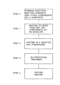
Fig. 1 is a flow chart of a method of
.... ... .
manufacturing an image-forming apparatus according to
the invention.
Figr 2 is a sectional view of an apparatus to
be used for the first and second steps of a method !of
manufacturing and image-forming apparatus according to
the invention.
Fig. 3 is a schematic perspective view o~ a
;~ surface conduction electron-emitting element to be
used for an image-forming apparatus according to the
.~
- 12 - ~ ~ 7 8
l invention.
Fig. 4 is a schematic sectional view of an
image-forming apparatus according to the invention.
Fig. 5 is a partially cut-out schematic
perspective view of an image-forming apparatus
according to the invention.
Fig. 6 is a schematic view illustrating a
simple matrix wiring arrangement of an electron~
emitting element to be used for an image-forming
apparatus according to the invention.
Fig. 7 is a schematic plan view of a ~
conventional surface conduction electron-emitting ~ ~-
. . . .::
element. -
Fig. 8 is a schematic plan view of another
15 conventional surface conduction electron-emitting -~
element. -- -
DETAILED DESCRIPTION OF T~E PREFERRED EMBODIMENTS : :-
A method of manufacturing an image-formi~ng - -~
apparatus according to the invention is characterized
- . - ~ :-
~firstly in that it comprises a step of hermeticallysealing an envelope formed by a plurality of members.~
More specifically, the hermetically~sealing step -
consists in heating the plurality of members for an
envelope to bond them together in an atmosphere
; containing at least a gas selected from reducing
gases, inert gases and non-reducing and non-oxidizing ~-
"'~ ''~
- 13 ~ 78
l gases or in a vacuum. Such a step can minimize the
formation of oxide film on the element electrodes of
each electron-emitting element and the wiring
electrodes connecting electron-emitting elements
during the process of manufacturing an image-forming
apparatus so that the disadvantage of an increase in
the element resistance and the wiring resistance of
each electron-emitting elements of a conventional ;,
image-forming apparatus manufactured by a known method
can be practically eliminated and consequently the
power consumption rate of the manufactured apparatus
can be m; n; mi zed.
Secondly, the above described hermetically
sealing step is'advantageous in that, if an even
I5 distribution of temperature is not rigorously observed
on the apparatus during the stept the disadvantage of
varied electron emission rates and consequent
improperly illuminated images on the display screen
of a conventi~nal image-forming apparatus due to the
formation of oxide film can be practically avoided.
Finally, if it is used to manufacture an
image-forming apparatus comprising surface conduction
electron-emitting elements, each having a electro-
conductive film including an electron-emitting region
(a thin film for electron emission) arranged between
a pair of electrodes, it can practically eliminate
the known disadvantage that the metal of th,e element
~ ll4~ 7
- 14 -
1 electrodes of the surface conduction electron-emLtting
elements of the appara~us is ap~ to be oxidized during : ::
the manufacturing process particularly at the inter~
faces of the thin ~ilm including an electron- ::
emitting region and the element electrodes of each
element to increase the electric resistance of the -:
element so that, at worst, no electricity may be -
allowed to flow therethrough, making the element : :
totally inoperative. If the operation of forming is
carried out for the surface conduction electron-
emitting elements after the above described
hermetically sealing step, the forming operation :
will not consume electric energy at any enhanced rate :~
unlike the case of any known comparable manufacturing :
15 methods because practically no oxide film is formed :~
and the electric resistance of the elements is not
:: raised during the hermetically sealing step. : :
If a method according to the invention is used ~
.. . ........ ... . .
to manufacture an image-forming apparatus comprising ;:~
20 surface conduction electron-emitting elements, each
: having a electroconductive film including an
electron-emitting region arranged between a pa:ir of! ~ ;
electrodes, it preferably comprises a step of heating ~
the thin fiIm for electron emission of each electron~ b
: 25 emitting element in an atmosphere cont~;n;ng at least :-~
one or more than one of the substantial elements of -:
the thin film for electron emission in addition to ~ ~
' " ;,~ ,'' ''''
-
1 the hermetically sealing step.
This is because an electron-emitting element
such as a surface conduction electron-emitting element
having a electroconductive film including an electron-
emitting region arranged between a pair o~ electrodescan be chemically affected by heat during the
hermetically sealing step so that a thin film for
electron emission having a desired chemical composition
may not be obtained after all. Therefore, by
employing a step of heating the thin film for electron
emission of each electron-emitting element in an
atmosphere containing at least one or more than one
of the substantial elements of the thin film for
electron emission in addition to the hermetically
sealing step, the thin film may come to show a desired
chemical composition becau~e of a thermochemical
reaction of the thin film for electron emission and
the gases in the atmosphere that takes place after
.. . ......... ...
the hermetically sealing step.
The above described heating step to be
conducted in a specific atmosphere is also advan-
tageous in that, while the thin film for electron
emission of each electron-emitting element such as a
surface conduc~ion electron-emitting element formed ~
25 between the electrodes of the element by spinner ~ ~ -
coating or vapor deposition of a chemical substance
may not show a desired and intended chemical -
: ~
- 16 - ~ 1 1 4 ~ ~ 8
~,., ,:
1 composition, this problem o~ formation of a thin film
having an undesired chemical composition can be
avoided by heating the thin film for electron ~
emission in an atmosphere containing at least one or ;--
more than one of the substantial elements of the thin
film for electron emission. For the above described
reasons, the heating step preferably comes after the
hermetically sealing step. -
: . -: , -
Now, the present invention will be described10 by way of a best mode o~ carrying out the invention.
Fig. 1 shows a flow chart of a method of
manufacturing an image-forming apparatus according ~-
to the invention. This flow chart may be appropri- ~-
ately used to manufacture an image-forming apparatus
as illustrated in Fig. 4.
Referring to Fig. L, in step 0, a plurality of
surface conduction electron-emitting elements, each
. , - -:
having an electron-emitting region generating thin
-
~film (thin film for electron emission), and wires ~or
feeding the elements with electric power are arranged
on a substrate. This step, or step 0, will be
described below in greater detail by referring to
Figs. 3 and 4.
The surface of a substrate 85 made of an
insulating material such as glass or a ceramic
substance is thoroughly cleansed in advance and a
plurality of surface conduction electron-emitting
' .~,' ~:;',
- 17 ~ 21~447~
1 elements 81 that have not been subjected to a forming
operation (an operation for generating an electron-
emitting region in each element) and each of which
has a configuration as schematically shown in Fig. 3
are arranged on the surface of the substrate 85.
In the course of this step, a film of a metal such as
Cu, Ni, Al or Ti is formed to a thickness of 500 to
5,000 angstroms by means of a known film forming
technique such as vapor deposition or sputtering and
a resist pattern is formed for a pair of electrodes
71, 72 of each element. Then, the film is etched to
produce the electrodes 71, 72 for each element that
are separated from each other by L, which is equal to
several microns. Note that the electrodes may
alternatively be prepared by using a technique called
lift-of~.
Thereafter, an electron-emitting region
generating thin film is formed to fill the gap betwee~ ~
the electrodes 71, 72 and partly cover the electrodes. -
The thin film typically has a length of several
hundred microns nad a width of tens of several -
microns. Althouqh the electron-emitting region
generating thin film is preferably made of a metal -
- selected from ~i, Nb, Sn, Cr, Zn, Rh, Hf and Pd, a
compound containing at least one of the above
mentioned metals, a semiconductiv~ substance such as
Si or Ge or a compound containing at least one of the
''' ~- '
- 18 - 2~ 7~ ~
1 above mentioned semiconductive substances, it may be
made of an appropriate material other than the above
substances if the electron-emi~ting region generating
thin film shows a resistance of several ohms to
several mega-ohms per unit square after the completion
of the second step, which will be described later.
While an electron-emitting region generating
thin film may preferably be prepared for the purpose
of the present invention by vapor deposition,
1~ sputtering or spinner coating of a solution
cont~;n;ng one of the above mentioned metals and
semiconductive substances or a chemica~ compounds
contA;ning such a substance, any other appropriate ;
method may alternatively be used. The electron-
.
emitting region generating thin film prepared in the
above step may be in the state of continuous film, -~
fine particles or a composite thereof.
Subsequently, a pattern of wires (not shown)
lS formed for feedlng the plurality of surface ~--
conduction electron-emitting elements 81 with
electric power. The material to be used for the
wlres is preferably a low resistance metal such as - ~ -
Cu or A1 and the pattern of wires typically has a ;~
thickness of several microns. The technique of
forming the electrodes 71, 72 may also be used for
producing the wire pattern. If the pattern of wires -~
is realized in the form of a simple matrix comprising
. . ~. .
-- 19 --
l a plurality of wires arranged along the direction of
X (EXl, EX2, ...) and those arranged along the
direction of Y (EYl, EY2, EY3, ...) as illustrated in
Fig. 6, an insulation layer may be disposed between
S each of the X-directional wires and each of the Y-
directional wires at and around the crossing thereof,
such insulation layers may be prepared in a manner as
they are formed in the course of manufacturing an
ordinary semiconductor device. Note that A in Fig.
6 denotes an electron-emitting element such as a
surface conduction electron-emitting element.
Step 1 in Fig. 1 is a step where the -
operation of hermetically sealing the envelope of an
image-formlng apparatus according to the invention
is carried out. As described earlier, this step
provides an image-forming apparatus accordiny to the ~-
invention with a very significant feature. Now, this
. ~- ,
hermetically sealing step will be described in greater
detail. While the envelope (panel~ comprises a face ~; -
plate 83, spaaers g2 and a substrate 85 in Fig. 4,
for the purpose of the present invention, the face
plate 83 and the spacers 82 or the spacers 82 and the
substrate 85 may alternatively be supplied as an
integrated single component that has been prepared in
25 advance. -~
Referring to Fig. 4, frit glass 86 is applied ~--
to the bonding areas of the face plate 83 carrying a -
-
2~ 8
- 20 -
.
l phosphor layer 84 and a metal back layer 88 in its
inner surface and/or those of the spacers 82 and the
face plate 83 and the spacers 82 are calcined along
with the applied frit glass 86 before they are
s baked and bonded together. Frit glass 86
is also applied to the bonding areas of the spacers -~
82 and/or those of the substrate 85 and then they ;~
are calcined. The calcining operation is necessary
to remove the organic binding agent contained in the
lo applied frit glass and normally conducted at a ~ ~-
temperature lower than the temperature at which the
baking operation is conducted. The latter operation ;
will be described later in greater detail. There-
after the assemblage of the face pIate 83 and the ;~
spacers 82 is properly aligned and firmly held to the
substrate 85~ and then these components are put into a ~-
furnace as illustrated in Fig. 2 which is provided
- ,, :.
with a container that can be airtightly sealed and
.... ,,,: :: :,,
evacuated to heat the entire assemblage contained
.~
20 therein and produce a complete envelope. -
Referring to Fig. 2, the furnace comprises
heating lamps 63 and a 'container 64 for containing !
an envelope 61 to be thermal1y processed therein,
said container 64 being provided with a support table
25~ 62, a stirrer 6~ for achieving an even distribution
of temperature within the container, a gas inlet
,
::
:
2 ~ 7 ~
1 port 66 equipped with a valve and an exhaust port
67 also equipped with a valve. The container can be
airtightly sealed and evacuated as described above
and its walls are made of a material that can transmit
beams irradiated from the heating lamps 63.
In operation, the valve of the exhaust port
67 is opened to evacuate the container 54 by means of
a vacuum pump (not shown) to a pressure of not
higher than 10 4 Torr. Once the intended degree of
vacuum is achieved within the container, the valve
of the exhaust port 67 is closed and the vale of the
gas inlet port 66 is opened to allow a reducing gas
such as H2 or CO, an inert gas such as He, Ar, Ne,
Kr or Xe, a non-reducing and non-oxidizing gas such ~
15 as N2, CO2 or CF4 or a mixture of any of these to ~ -
enter the container and shows a pressllre between -- b
several to several thousand torrs inside the container ~ -
although the inside pressure of the container is --
normally held to a level equal to the atmospheric --
20 pressure. Note that the atmosphere in the container ~
prevails the inside of the envelope 61 and the -~-
pressure of the inside of the envelope 6,1 is held ! '
equal to that of the inside of the container 64
during this step because the exhaust pipe 87 is not
sealed yet. Also note that the container 64 may be
heated in a vacuum without filling it with gas and
using a stirrer if an even distribution of temperature -
" . . .
:: ~
--~ 2 ~ 7 8
- 22 -
1 is not required within the container 64.
Thereafter, the heating lamps 63 are energized
to heat the inside of the container 64 at a temperature
appropriate for melting the frit glass which is
typically 450~C for approximately an hour, while
operating the stirrer 65. Subsequently, the envelope ; ;~-
is slowly and gradually cooled to ambient temperature.
Referring again to Fig. 1, step 2 is a step
where the thin film for electron emission of the
apparatus is heated in an atmosphere containing at
least part of the elements that constitute the thin ;
film. This step will now be described below in ;
greater detail.
As in step 1 described above, the container 64 - ~
15 is evacuated to a pressure of not higher than 10 4 - ;-
Torr. Then, the valve of the exhaust port 67 is
alosed and that of the gas inlet port 66 is opened ~ -~
to allow gas inter the container, said gas being
capable of thermochemically change the metal or the
semiconductor contained in the thin ~ilm for electron
emission 73 prepared in step 0 to a substance that
can emit electrons. Thus, an oxidizing gas such asi ~ ;
~2 or N02 will be suitably used to produce a thin
film of an oxide such as SnO2 or PdO, whereas N2 or
NH3 will be introduced into the container if a thin
film of a nitride needs to be prepared. The gas
::
pressure in the container 64 is held to several to
- 23 ~ 21~ ~ 47 8
1 several thousand torrs although the inside pressure
of the container is desirably equal to the atmospheric
pressure. Note again that the atmosphere in the .
container prevails the inside of ~he envelope 61 and
the pressure of the inside of the envelope 61 is held
equal to that of the inside of the container 64 during
this step because the exhaust pipe 87 is not sealed ~.~
yet. The heating temperature in step 2 needs to be ~: -
equal to or higher than the temperature at which a
desired chemical compound for electron emission is
formed and, at the same time, it needs to be not
higher than the temperature at which the material of
the electrodes 71, 72 chemically reacts with the
gas introduced into the container 64 and produces an
15 insulating compound if such a chemically reactive : -.
material is used for the electrodes 71, 72. For ;
example, if the electrodes 71, 72 are made of Ni and
PdO is produced in an ~2 atmosphere for electron
emission, the heating temperature needs to be between
150~ and 320~C. Then, the heating operation will be
continued for several minutes to several hours and,
subsequently, the image-forming apparatus will~ be
allowed to become sufficiently cold before it is
taken out of the furnace. - :
~ 25: It should be noted that, while a furnace : :
; ~ having a configuration as illustrated in Fig. 2 is
used in the above description, a furnace of any other
24 '~ 7 X
l type may alternativ~ly be used if an image-forming ~; ;
apparatus according to the invention can be heated
in a desired atmosphere to a desired temperature for
a given period of time.
Thereafter, step 3 takes place. In this step,
the image-forming apparatus in the container is
evacuated by means of an exhaust pipe 87 and a ;-
vacuum pump such as a turbo molecular pump (not ~ ;
shown) to achieve a pressure of not higher than lO 6
Torr within ~he apparatus. Then, the electron-
emitting re~ions 74 of the apparatus are formed by
applying a voltage of several to tens of several
volts to the electrodes 71, 72 of each electron-
emitting element by way of wires. ~ ~
Subsequently, step 4 is carried out. In this ~ -
step, the image-forming apparatus is heated by
heating means such as a hot plate (not shown) to a
temperature that does not cause the material of the
electron-emitting elements which is typically an
oxide or nitride to be reduced and then evacuated by
means of the exhaust pipe 87 over several days to
achieve a pressure of not higher than 10- 6 Torr
within the image-forming apparatus. After the
getter (not shown) that has been arranged in the
vacuum container contA;n;ng the image-forming
apparatus is made to evaporate, the exhaust pipe 87
is heated and sealed by means of a gas burner.
~:
- 25 - 2~
: ~'
l At the end of step 4, the image-forming
apparatus is finished, although steps 1 and 2 provide ~ ;
a remarkable feature to a method of manufacturing an
image-forming apparatus according to an aspect of the
.
invention and, therefore, the remaining steps are
not limited to those described above. ' -
Now, the present invention will be described ~ ;~
further by way of examples. ~ :-
[Example 1]
A sample image-forming apparatus having a
configuration as shown in Fig. 4 and comprising an
electron source having a large number of surface
conduction electron-emitting elements arranged in
array was prepared by a method according to an aspect
of the invention.
PdO was used for the electron-emitting region
forming thin film 73 of each surface conduction
electron-emitting element shown in Fig. 3.
~:-
Now, the process of preparing this sample of
image-forming apparatus will be described below
in detail.
f In terms of each surface conduction electron-
emitting element, a pair of nickel element electrodes
71, 72 were firstly formed on a glass substrate by ~-~
lift-off to a thickness of l,000 angstroms. The
electrodes were separated from each other by a gap
which was 400 microns long and 2 microns wide.
, . . . ,:~ - . . .
' ~, ' ' ' ': '-- '-:
- 26 - % ~ 7~
.
l Then, an organic Pd solution (Catapaste ccp:
available from Okuno Pharmaceutical Industries Co., ~;
Ltd.) was applied to the assemblage of the element
electrodes by spinner coating and the substrate,
which were subsequently baked at 300~C for fifteen
minutes.
Thereafter, the assemblage of the element
electrodes and the substrate was subjected to a
patterning operation using a resist pattern and then ;~ ;
an etching operation to produce an electron-
emitting region generating thin film 73 to fill the
gap between the element electrodes 71, 72 and partly
cover the element electrodes. The thin film 73 was
principally made of PdO and hàd a length of 280
microns along the gap and a width of 30 microns.
A total of 600x400 identical elements were
arranged on the glass substrate in the form of a
matrix, although~they had not an electron-emitting
region on each of them yet.
Then, another patterning operation using a
resist pattern and a subs~quent etching operation were
carried out to wire the~elements with an aluminum -~
~wire pattern having a thickness of 1 micron.
Thereafter, the process of preparing the
25 sample proceeded to step 1. -;~
Referring to Fig. 4, frit glass 86 (LS-0206
available from Nippon Electric Glass Co~, Ltd.) was
2 ~ 7 8
- 27 ~
1 applied to appropriate areas o~ a face plate 83 on ~-
which a phosphor layer and 2 metal back layer had been :
formed to give it electroconductivity and 5 mm long -~
spacers 82, which were subsequently calcined at 400~C
for ten minutes and then baked at 450~C for an hour
to firmly bond the spacers 82 to the face pla~e 83.
Then, frit glass 86 was applied to appropriate areas
of the spacers 82 that were to be put to contact with
the substrate 85 and subsequently calcined at 400~C
for ten minutes.
Then, the member that had been produced by
assembling the face plate 83 and the spacers 82 and
the substrate 85 carrying the matrix of the elements
81 were aligned relative to aach other to form an
envelope (panel), which was then placed in a furnace
as illustrated in Fig. ~. The container of the
furnace of Fig. 2 was evacuated to a pressure of not
higher than 10 4~Torr and thereafter a gaseous
mixture of N2 (90%) and H2 (10~? was introduced into
the container to maintain the inside pressure of the
,- -.:: ~':
: container equal to the a~mospheric pressure. Then,
the stirrer 65 was operated and the heating lamps ! '
were energized to heat the envelope at 450~C for an ~ -
- hour, at the end o~ which aIl the components of the
2S envelope were firmly bonded together by molten frit - -
glass 86. .-~
Thereafter, step 2 was carried out for the
"',,, ~; ~,~,,,'
-~ 2il~78 ~- ;
- 28 -
1 process of preparing the sample.
The envelope was cooled to 50~C in the -
container 64, which was then evacuated to a pressure
of not higher than 10 4 Torr. Subsequently, ~2 gas
was introduced into the container 64 to maintain the
inside pressure of the container equal to the
atmospheric pressure. Then, the stirrer 65 was
operated and the heating lamps were energized to heat
the envelope at 320~C for an hour, at the end of
which the electron-emitting region forming thin film
73 of each element was found to have been oxidized.
Thereafter, the envelope was cooled to room
temperature and the envelope was taken out of the
furnace. When tested, each element of the image-
forming apparatus showed a level of electricresistance between 200 and 300 ohms, which was
substantially equal to the electric resistance af an
element that had not been heated in steps 1 and 2. ~ ~-
.... . ~ : :
Then, the envelope was evacuated by means of
the exhaust pipe 87 and a turbo molecular pump (not
shown~ to a pressure of not higher than 10 6 Torr. ~-
Subsequentlyj a voltage of 5V was applied to the pair
of element electrodes 71, 72 of each element of the
image-forming apparatus by way of appropriate wires
so that each element was subjected to an electrifi-
cation treatment using an electric current of ~ -
approximately 20mA to finally produce an
~: '
2 ~ 7 8
- 29 - -
1 electron-emitting region 74 in the electron-emitting
region generating thin film 73 of the element.
Thereafter, the envelope was heated to
approximately 130~C by means of a hot plate and then
S evacuated to a pressure of not higher than 10 6 Torr
over several days. After the getter (not shown~ that
had been arranged in the vacuum container cont~; n; ng
the image-forming apparatus was made to evaporate,
the exhaust pipe 87 was heated and sealed by means of
a gas ~urner.
When the finished image-forming apparatus
was connected to a drive circuit to make it display
images, it was found that the displayed images showed
a high degree of evenness in the brightness with a
lS deviation of only about 8%.
[Comparative Example 1] -~-
- ~ ~ In order to evaluate the sample image forming ~ --
apparatus of Example l above, a similar apparatus was
prepared for~comparison by following the process of -
~ 20 Example 1 except that air was used in place of the
; ~ mixture gas of N2 and H2 in step 1 to provide an ~
atmosphere fcr the bonding operation using molten ~ -
~ ., ::: .
~ frit glass 86, although the inside pressure of -the ~-
... . .
container was held equal to the atmospheric pressure
and that step 2 was completely omitted.
When the sample for comparison was cooled to ~-
room temperature and taken out of the container to
;, ,~
., ,-
:
:,
-: :
~ 30 ~ 2i~ ~ 47 8
l determine the electric resistance of each element 81
of the apparatus a~ter its major components had been
bonded together with molten frit glass 86 in the
container filled with air to show a pressure equal
to the atmospheric pressure, it was discovered that
the elements 81 had an enhanced electric resistance
ranging from l up to 500kohms, revealing a wide
variance existing there. When each element of the
apparatus was subjected to an electrification
treatment to produce an electron-emitting region 74
out of its electron-emitting region generating thin
film 73, the required electric power was twice to five :.
times greater than the power used for Example 1.
When the finished image-forming apparatus was -
15 connected to a drive circuit to make it display ; :
~ images, it was found that the displayed images
"
: showed a poor degree of evenness in the brightness :~:
:~ with a deviation of approximately as high as 50~
. :: ,-, . : -~:
[Example 2]
A sample image-forming apparatus having a
:
configuration as shown in Fig. 4 and comprising an
electron~source having a large number of surface ! ' ' .
; conduction electron-emitting elements arranged in
array was prepared by a method according to another
:: .
~:: 25 : aspect of the invention.
SnOX :~x=l to 2) was used for the electron-
. emitting region generating thin film 73 of each
... .. . . ..
21~478
- 31 -
1 surface conduction electron-emitting element shown in
Fig. 3
Now, the process of preparing this sample of
imaye-forming apparatus will be described below in
s detail.
In terms of each surface conduction electron-
emitting element, a pair of chromium element electrodes
71, 72 were firstly formed on a glass substrate by
lift-off to a thickness of 1,000 angstroms. The
electrodes were separated from each other by a gap
which was 400 microns long and 2 microns wide.
Then, a film of Sn was formed on the assemblage -
of the element electrodes and the substrate by
electron beam vapor deposition to a thickness of 100
angstroms~ Therea~ter, the assemblage was subjected
to a patterning operation using a resist patt:ern and
then an etching operation to produce an electron- ~ - -
~emitting region generating thin film 73 to fill the
...... ... ..... ", ~,
gap between the element electrodes 71, 72 and partly
cover the eIement electrodes. The thin film 73 was
. :,
principally made of SnOx (x=l to 2) and had a length ~ -
of 280 microns along the gap and a width of 30
microns.
A total of 600x400 identical elements were ~-
25 arranged on the glass substrate in the form of a f
- ~:
matrix r although they had not an electron-emitting
region on each of them yet. -~
- 32 _ 21~4478
1 Then, another patterning operation using a
resist pattern and a subsequent etching operation
were carried out to wire the elements with an
aluminum wire pattern having a thickness of 1 micron.
Thereafter, the operations of step 1 were
carried out in a ~nn~r same as in the case of Example
1 except that Ar gas was used in place of the mixture
gas of N2 and H2 to maintain the inside of the
container to the atmospheric pressure.
Subsequently, ~he operations of step 2 were ~ -
carried out in a manner same as in the case of Example -~ -
1 except that NO2 gas was used in place of ~2 gas to
maintain the inside of the container to the atmospheric -- ;
..,: . ::.
pressure and that the assemblage was heated at 300~C
15 for an hour to produce an electron-emitting region ~ -
generating thin film 73 for each element.
Then~an image-forming apparatus was prepared
as in the case of Example 1.
When the finished image-forming apparatus was
connected to a drive circuit to make it display~
images, it was found that the displayed images showed
a high degree of evennass in the brightness with a !
deviation of only about 9~.
[Comparative Example 2]
In order to evaluate the sample image-
forming apparatus of Example 2 above, a similar
apparatus was prepared for comparison by following -
~ 33 ~ 211~78
1 the process of Example 1 except that air was used
in place of the Ar gas in step 1 to provide an
atmosphere for the bonding operation using molten frit
glass 86, although the inside pressure of the : -
5 container was held equal to the atmospheric pressure ;-
and that step 2 was completely omitted.
When the sample for comparison was cooled to
room temperature and taken out of the container to
determine the electric resistance of each element 81 -
10 of the apparatus after its major components had been ; ;~;
bonded together with molten frit glass 86 in the
container filled with air to show a pressure equal to -
the atmospheric pressure, it was discovered that
the elements 81 had an enhanced electric resistance
15 ranging from 2 up to lOOkohms, revealing a wide ;~ --
variance existing there. When each element of the -: -
apparatus was subjected to an electrification
treatment to produce an electron-emitting region 74
out:of its electron-emitting region generating thin
film 73, the required electric power was three to
eight times greater than the power used for Example
2.
When the finished image-forming apparatus was
connected to a drive circuit to maXe it display images,
:25 it was found that the displayed images showed a poor
degree of evenness in the brightness with a deviation
of approximately as high as 60%. .
2 ~ 7 ~
- 3~ -
1 [Example 3]
A sample image-forming apparatus having a
configuration as shown in Fig. 4 and comprising an
electron source having a large number o~ surface
conduction electron-emitting elements arranged in
array was prepared by a method according to still
another aspect of the invention.
ZnNx (x=l to 2) was used for the electron-
emitting region generating thin film 73 of each ~;
surface conduction electron-emitting element shown
in Fig. 3.
Now, the process of preparing this sample of
image-forming apparatus will be described below in
detail.
In terms of each surface conduction electron-
emitting element, a pair o~ copper element electrodes
71, 72 were firstly formed on a glass substrate by
lift-off to a thickness of 1,000 angstroms. The
electrodes were separated from each other by a gap
which was 400 microns long and 2 microns wide.
~hen, a film of Zn was formed on the
assemblage of the element electrodes and the -
substrate by ion beam vapor deposition to a thickness
of 80 angstroms. Thereafter, the assemblage was
subjected to a patterning operation using a resist
pattern and then an etching operation to produce an
electron-emitting region generating thin film 73 to
'-"' 21~78
- 35 -
1 fill the gap between the element electrodes 71, 72
and partly cover the element electrodes. The thin ~
film 73 was principally made of Zn and had a length ~-'
of 280 microns along the gap and a width of 30
microns.
::: - .,
A total of 600x400 identical elements were
arranged on the glass substrate in the form of a ~ -
matrix, although they had not an electron-emitting
region on each of them yet.
Then, another patterning operation using a ;~-
resist pattern and a subsequent etching operation
were carried out to wire the elements with an ~'~
aluminum wire pattern having a thickness of 1 micron.
:
Thereafter, the operations of step 1 were ~
. ..: :
carried out in a n'nn~r same as in the case of Example
1 except that CO gas was used in place of the mixture ~ '
gas of N2 and H2 to maintain the inside of the
container to the atmospheric pressure.
Subsequentlyl the operations of stap 2 were
20 carried out in a manner same as in the case of - ~-
Example 1 except that N2 gas was used in place of ~2
gas to maintain the inside of the container to the ,
atmospheric pressure and that the assemblage was
heated at 300~C for an hour to produce an electron-
emitting region forming thin film 73 for each
~ :.-
element.
It should be noted that, when ZnNx is used
' ~
~,
- 36 - 2~ 78 :~
1 for an electron-emitting region forming thin film,
the operations of step 2 will be most successfully
carried out by following those of this example
because a ZnNx film can hardly be processed for
patterning particularly in the initial stages.
Then an image-forming apparatus was prepared
as in the case of Example 1.
When the finished image-forming apparatus
was connected to a drive circuit to make it display
images, it was found that the displayed images showed
a high degree of evenness in the brightness with a
deviation of only about 8%.
[Comparative Example 3]
An apparatus similar to that of Example 3
was prepared for comparison by following the process
: of Example 3 except that air was used in place of the
CO gas in step 1 to provide an atmosphere for the
bonding operation using molten frit glass 86,
although the inside pressure of the container was
held equal to the atmospheric pressure and that step
: ~ 2 was completely omitted.
When the finished image-forming appàratus was
connected to a drlve circuit to make it display
~: images, it was found that the displayed images showed
~ 25 a:poor degree of evenness in the brightness with a
:~ deviation of approximately as high as 50
[Example 4] ~ ~
~. .
- 37 - 211~8 ~ ;~
, . .
l In the example, a sample image-forming ;- -
apparatus was prepared in a m~nner same as in the -
case of Example l, although the operations of step l -
were carried out in vacuum.
Then, the operation of hermetically sealing
.: .
the envelope (panel) of the sample apparatus was
carried out as in the case of Example l except that,
.
after placing the envelope in the container 64 of a
furnace as shown in Fig. 2, the container 64 was
evacuated to a pressure of not higher than lO 4 Torr
and thereafter the heating lamps 63 were energized to
heat the apparatus at 450~C for an hour in order to ~ ~
melt the frit glass 86 and bond the related compo- -
nents together.
When the finished image-forming apparatus was
connected to a drive circuit to make it display images,
it was found that the displayed images showed a high
degree of evenness in the brightness with a deviation
.. . ................... .
of only about 8%. ~
::
[Advantages of the Invention]
As described above in detail, according to
the invention, there is provided a method of manu-
facturing an image-forming apparatus that can display '~
high quality images and operate with a reduced rate
of power consumption and a reduced variance in the
rate of electron emission among a plurality of
electron-emitting elements arranged therein for
- ': '
:: ', '
- 38 - '~ 478
1 image display by minimi2ing the production of oxide
film in the operation of melting frit glass and
bonding the related components of the apparatus
(the operation of hermetically sealing the envelope
of the apparatus). An image-forming apparatus
manufactured by such a method also constitutes part
of the present invention.
In particular, according to the invention,
there is provided a method of manufacturing an image-
forming apparatus comprising surface conductionelectron-emitting elements that can display high
quality images and operate with a reduced rate of
power consumption. An image-forming apparatus
manufactured by such a method also constitutes part of
the present invention.
-~
' ~'' .
~ 25 ~
; ~ ~
,'' '~.'' ~'