Note: Descriptions are shown in the official language in which they were submitted.
CA 02114~63 1997-12-0~
INTEGRATED SEMICO~ LOR DEVICES
AND METHOD FOR MANUFACTURE THEREOF
BACRGROUND OF THE Ihv~NllON
This invention relates to bonding of fully-
fabricated semiconductor devices onto other fully-
fabricated semiconductor devices so as to produce
integrated units, and particularly to bonding fully-
fabricated photonic elements, such as GaAs/AlGaAs multiple
quantum well (MQW) modulators, onto fully-fabricated
integrated circuit (IC) chips such as Si or even GaAs.
Integration of photonic devices with silicon IC
chips makes it possible to combine the advantages of each.
Among photonic devices, GaAs/AlGaAs multiple quantum well
(MQW) modulators are particularly beneficial as
input/output (I/O) elements on IC chips because they have
a high absorption coefficient of light and can serve as
both receivers and transmitters. They typically operate at
an optical wavelength (A) of 850 nm (nanometers).
Growing GaAs/AlGaAs on fully-fabricated IC chips
has proven difficult because it subjects the IC chips to
damage. On the other hand, techniques exist for bonding
fully-fabricated semiconductor devices to each other.
However, these leave the substrates of each device in
place. This subjects the bonds to adverse mechanical
stresses that may affect the devices adversely. In the
case of GaAs/AlGaAs multiple quantum well (MQW) modulators,
the substrates are GaAs which are opaque to the operating
wavelength of the GaAs/AlGaAs modulators, and hence require
removal for operation. Nevertheless, it is very difficult
to place and bond GaAs/AlGaAs multiple quantum well (MQW)
modulators, if they have had their substrates removed, onto
silicon IC chips. Prior techniques for bonding
fully-fabricated semiconductor devices to each other, and
~ ~ ~4563
in particular multiple quantum well (MQW) modulators to
silicon IC chips, suffer the disadvantages of mechanical
stress, opacity, or cumbersome handling.
An object of the invention is to overcome these
disadvantages.
Another object of the invention is to improve
bonding of semiconductor devices with each other.
Another object of the invention is to improve
bonding of photonic elements with electronic elements.
SUMMARY OF THE lN V~N-LlON
According to a feature of the invention we achieve
such objects by bonding the conductors of one fabricated
semiconductor device having a substrate to the conductors
on another fabricated semiconductor device having a
substrate, flowing an etch-resist between the devices,
allowing the etch-resist to dry, and removing the substrate
from one of the semiconductor devices.
According to another feature of the invention, one
semiconductor device is a device having one or more
GaAs/AlGaAs multiple quantum well modulators and the other
semiconductor device is an IC chip, and the substrate on the
device with the GaAs/AlGaAs multiple quantum well modulator
is removed.
According to another feature of the invention, the
etch-resist is a photoresist and is left to impart
mechanical strength to the device.
According to another feature of the invention, the
etch-resist is removed.
In accordance with one aspect of the present
invention there is provided the method of forming an
integrated semiconductor device, comprising the steps
of: bonding conductors of a first semiconductor device
having a substrate to conductors on a second semiconductor
device having a substrate; flowing an etch-resist to fill
A
S 6 ~
2a
a space between the first semiconductor device and the
second semiconductor device; allowing the etch-resist to
dry; and removing the substrate from the second
semiconductor device.
In accordance with another aspect of the present
invention there is provided an integrated semiconductor
device, comprising: a first semiconductor device having a
substrate and with conductors; a second semiconductor device
without a substrate and with conductors; said conductors on
said first semiconductor device being bonded to said
conductors on said second semiconductor device; and an etch-
resist extending between said first and said second
semiconductor devices.
These and other features of the invention are
pointed out in the claims. Other objects and advantages of
the invention will become evident from the following
detailed description when read in light of the accompanying
drawings.
CA 02114~63 1997-12-0
BRIEF DESCRIPTION OF THE DRAWINGS
Fig. 1 is a cross-sectional view illustrating a
photonic device in the form of-an MQW modulator containing
a multiple quantum well modulator unit.
Fig. 2 is a cross-sectional view illustrating an
arrangement in a step for forming a device that integrates
the multiple quantum well modulator with an integrated
circuit chip according to features of the invention.
Fig. 4 is a cross-sectional view illustrating a
device integrating a photonic element with an electronic
element and embodying features of the invention.
Fig. 5 is graph illustrating the reflectivity
spectra of the MQW modulator embodying the invention under
different reverse biases.
Fig. 6 is a cross-sectional view illustrating a
device integrating a number of photonic elements on an IC
and embodying features of the invention.
Fig. 7 is a plan view illustrating a device
integrating an array of photonic elements on an IC and
embodying features of the invention.
DETAILED DESCRIPTION OF PREFERRED EMBODIMENTS
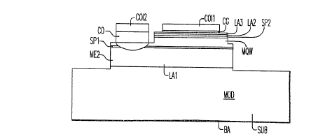
Figs. 1-4 illustrate a GaAs/AlGaAs 850 nm A
multiple quantum well modulator MOD, and a solder-bonding
technique for integrating the GaAs/AlGaAs 850 nm A
modulator with an IC to form the device embodying the
invention. Fig. 1 illustrates a multi-strata multiple
quantum well modulator MOD for bonding to contacts on a Si
device according to the invention.
2114563
In the modulator MOD, a GaAs substrate SUB
supports a 1.5 ~m layer LAl of n (i.e. n-doped) (1013 cm~3)
Alo3Ga07As grown on the substrate SUB. A 100 A i (i.e.
intrinsic) Alo3GaO 7As spacer SP1 on the layer LAl spaces
the latter from an i multiple quantum well modulator unit
MQW composed of 55 periods of 90 A GaAS wells and 30 A
Alo 3Ga0 7As barriers. A 70 A i Alo 3Ga0 7As spacer SP2 on the
multiple quantum well modulator unit MOW spaces the latter
from a 500 A p (i.e. p-doped) (1013 cm~3) AlxGalxAs layer LA2
graded from X=0.3 to x=0, on the spacer SP2. A 500 A p+
(5*1o13 cm~3) GaAs layer LA3 covers the layer LA2.
The modulator MOD, at the substrate SUB, forms a
5 mm square piece and has 110x110 ~m gold p contacts CG
(1000 A thick) deposited on the layer LA3. The strata MQW,
SP2, LA2, LA3, and CG form a 130x130 ~m inner mesa ME that
extends to within 1500 A of the n layer LA1. A 50x120 ~m,
7000 A thick, AuGe/Au n contact CO on the n layer LAl
extends upwardly to make its top coplanar with the gold p
contact CG. 4000 A In caps COI1 and COI2 cover respecti~e
contacts CG and CO.
Manufacture of the modulator MOD utilizes gas-
source molecular beam epitaxy. The structure in Fig. 1, is
manufactured according to the following steps:
- Growing the GaAs substrate SUB.
- Growing the 1.5 ~m layer LAl of n (i.e. n-
doped) (1013 cm~3) Alo 3GaO.7As on the substrate SUB.
- Growing the 100 A i Alo 3Ga0 7AS spacer SPl on
the layer LA1.
- Growing, on the spacer SP1, the i (i.e.
intrinsic) multiple quantum well modulator unit MQW
composed of 55 periods of 90 A GaAS wells and 30 A
Alo 3Ga0 7As barriers.
- Growing the 70 A i Alo 3Ga0 7AS spacer SP2 on the
multiple quantum well modulator unit MOW.
21~456~3
-
- Growing the 500 A p (p-doped) (10l8 cm~3) AlxGa
~As layer LA2 graded from X=0.3 to x=0, on the spacer SP2.
- Growing the 500 A p+ (5*1013 cm~3) GaAs layer LA3
on the layer LA2.
The procedure continues with:
- Processing the edges to the 5 mm square piece
of the modulator MOD to the shape shown in Fig. 1.
- Depositing the 110x110 ~m gold p contacts CG
(1000 A thick) on the layer LA3.
- Etching the 130x130 ~m inner mesa MEl around
the gold contacts to within 1500 A of the n layer LAl as
shown in Fig. 2.
- Deposition of the 50x120 ~m, 7000 A thick,
AuGe/Au n contact CO on the n layer LAl. The contact CO is
that thick in order to make its top coplanar with the gold
p contact CG. - Deposition of the 4000 A In caps
CA on both contacts CG and CO.
- Etching the 200x200 ~m outer mesa ME2 down into
the substrate SUB.
- Alloying the contacts CG and CO at 420~C for 1
minute.
- Thinning the modulator MOD to 200 ~m.
- Polishing the back of the substrate SUB for
viewing through an infrared microscope.
This completes the modulator MOD. Fig. 2
illustrates the modulator MOD upside down in position above
a portion of a Si device SD, such as an IC chip, as a step
in formation of the integrated hybrid device embodying the
invention. In Fig. 2 the device SD includes a 1 cm square
p type Si substrate SIS with Al contacts COAl and COP2 of
the same size and spacing as the p and n contacts CG and CO
on the modulator MOD. These Al contacts COAl and COA2 are
set to extend out of the page of Fig. 2 so that they would
be exposed when the hybridization process is completed
4~3
according to an embodiment of the invention. Indium
contacts CI1 and CI2 on the Al contacts also have the same
size and spacing as the modulator contacts CG and CO.
To integrate the modulator MOD with an IC chip, the
following occurs:
- Patterning a 1 cm square p type Si substrate SIS
with Al contacts COA1 and COA2 of the same size and spacing
as the p and n contacts CG and CO on the modulator MOD.
These Al contacts COA1 and COA2 are set to extend out of the
page of Fig. 2 so that they would be exposed upon completion
of the hybridization process according to an embodiment of
the invention.
- Depositing indium contacts COI1 and COI2 on the
Al with the same size and spacing of the modulator contacts
CG and CO.
- Placing the modulator MOD upside down on the Si
piece and aligning it. According to an embodiment of the
invention, a precision controller aligns the modulator MOD
on the Si device SD.
Fig. 3 shows the modulator MOD on the Si device SD
with the In contacts COI1 and COI2 bonded to the contacts
CI1 and CI2. Here AZ 4210* photoresist PH surrounds the
contacts CG, CO, COI1, COI2, COA1, COA2, CI1 and CI2. The
structure in Fig. 3 is achieved by the following steps.
- Heating the unit to 200~C for 15 minutes to melt
the indium contacts into each other. At this point the
resulting unit is relatively stable (i.e., shaking does not
cause it to break apart).
- Flowing AZ 4210* photoresist between the modu-
lator MOD and the Si device SD by depositing drops of
photoresist PH on the Si substrate about the GaAs/AlGaAs
modulator MOD and allowing it to flow against its edge.
- Air drying the photoresist PH for 12 hours. The
dried photoresist PH serves two purposes. First, it
* Trade mark
211~3
protects the MOD during substrate etching. Second, it
provides additional mechanical support.
Fig. 4 illustrates a structure embodying the
invention. Here an AR coating covers the MQW modulator MOD
and the surrounding photoresist PH. This structure is the
result of the following steps.
- Placing a drop of KOH solution on the surface
of the exposed GaAs to remove any GaAs oxide.
- Chemically removing the GaAs substrate from the
modulator MOD with a jet etcher ET by delivering a lxl mm
jet of etchant onto the surface of the substrate SUB. The
etchant is 100:1 H2O2:N~OH, which stops on the Alo3Ga0 As
layer LA1. The GaAs etchant ET does not attack the
photoresist appreciably nor Si or Al to the sides of the
GaAs/AlGaAs modulator. However, care is taken to quickly
deliver the unitary structure into the etchant jet after
applying the KOH, because KOH does attack photoresist. The
etchant etches the substrate S~3 in about 1.5 hours.
To prepare the integrated hybrid unit for use,
the Al contacts sticking out from underneath the modulators
are probed by poking the probes through the photoresist.
These probes then provide connections to the terminals on
the hybrid structure.
According to an embodiment of the invention, bond
pads extend to the edge of the silicon and the photoresist
is applied without coating them. According to another
embodiment of the invention, the chip is wire-bonded and
packaged before commencing the process.
After wire-bonding the Al pads of a modulator
~OD, an SiOx AR-coating AR is deposited. The gold p
contact served as an integral reflector.
Yet another embodiment of the invention involves
selective photo-chemical removal of the photoresist PH at
the bond pads.
211~ 63
Another embodiment includes using a solvent to
remove the photoresist completely. This leaves the
integrated device of Si chip and modulator MOD without the
mechanical support of the etch resist, but also without the
mechanical burden of the substrate S~B.
Samples of the integrated hybrid unit have been
fabricated with the photoresist remaining on the structure.
In tests made, it was possible to completely remove the 5x5
mm substrate without damaging any section. Since the outer
mesas of the modulators MOD were etched into the substrate
the photoresist PH completely isolates the integrated
structure. According to an embodiment of the invention,
the single modulator MOD and the single connection to the
Si device SD of Figs. 1 to 4 represents but one of a number
of an array of modulators MOD. Each of the latter is grown
on a single substrate and bonded to corresponding contacts
on the device SD with the single substrate SUB then
removed.
Fig. 5 shows the reflectivity spectra of a
modulator MOD under different reverse biases, measured with
a lamp/monochromator. Near an optical wavelength of 850
nm, a reflectance change from 52~ to 26~ occurs for a o to
10 volt bias swing.
Fig. 6 is a cross-sectional view illustrating a
device integrating a number of photonic elements with
electronic elements of an IC chip and embodying features of
the invention. Here, a number of modulators MOD, identical
to the modulators MOD in Fig.4, are bonded via bonded
contacts CN collectively representing the contacts CG, CO,
COI1, COI2, COAl, COA2, CI1 and CI2 to the substrate SIS of
a Si device SD. The bonding process is the same as the
process in Figs. 2 to 4 except that all the modulators MOD
start on a single substrate SUB and the Si device includes
a number of conductor pairs each matching the conductor
211~563
.
g
pair of the modulator MOD above that pair. Photoresist PH
extends between and around the contacts CN and the
modulators MOD. A single previously-removed substrate S~3
for the modulators MOD appear in phantom lines. The
photoresist PH also extends between the substrate SIS and
the level of the removed substrate SUB.
Fig. 6 shows a single line of modulators MOD.
The invention contemplates two dimensional arrays of such
modulator MOD as shown in Fig. 7. Because optical
input/outputs (I/0's), such as the multiple quantum well
modulators MOD, permit transmission and reception normal to
the surface of the chip, such two-dimensional arrays offer
substantial possibilities for use in hybrid communication
and information processing environments.
According to another embodiment of the invention,
the photoresist PH is removed from the structures of Figs.
6 and 7.
In operation, the output of an off-chip laser
splits into an array of spots and focuses on the multiple
quantum well modulators MOD, whose reflectance is modulated
by the on-chip electronics. This type of system offers the
advantage of having a global clock (for oscillating the
laser). In addition, it is because such m~dulators are
also efficient detectors that the one modulator can
function as both receiver and transmitter.
The invention furnishes a technique for solder-
bonding one semiconductor device onto another and removing
the substrate from one. In particular the invention
provides a method of bonding GaAs/AlGaAs 850 nm ~
modulators onto silicon. According to an embodiment of the
invention this technique forms whole arrays of devices in
one step. This technique provides a method for
optoelectronic integration of silicon IC's.
The invention enables the substrate of the
2114363
optical GaAs/AlGaAs modulator to be removed after it is
solder-bonded to a silicon chip. Removal of the substrate
is necessary since it is opaque to light at the wavelength
needed for operation. In addition, substrate removal
alleviates mechanical constraints on the bond. The
invention involves flowing of an etch-resist, such as a
photoresist, between the chips to allow etching of the
substrate. The flow may be enhanced by capillary action.
The photoresist protects the front sides of the chips
during etching and augments mechanical support. The
technique has survived several tests of robustness and will
support fabrication of large arrays. Although simple, the
invention permits the joining of complex electronic
circuits with optical inputs and outputs in large numbers.
The invention involves GaAs/AlGaAs p-i-n multiple
quantum well modulators solder-bonded to a silicon
substrate. The GaAS substrate is chemically removed to
allow operation at an optical wavelength of 850 nm. The
gold contact to the modulator is used as the reflector.
The invention achieves a change in reflectivity from 26~ to
52~ for 0 to 10 volts bias swing.
The invention promotes the use of photonics in an
information processing environment where it is integrated
with electronics. The invention takes advantage of the
greater capacity of electronics for complexity,
functionality, and memory, and the greater capacity of
photonics for communications. The photonic devices, such
as the multiple quantum well modulators, function as
optical interconnects between electronic integrated circuit
chips (IC's). The invention involves the integration of
photonic elements (both receiver and transmitter) on the IC
chip. It takes advantage of the attractive feature of
optical input/output (I/0) that it can occur normal to the
surface of the chip, and allow two-dimensional arrays of
~ ~ ~ 4 5 1~
11
interconnects to be formed, for surface-normal photonic
operation.
The invention takes advantage of silicon
electronic's effective technology where complex systems such
as microprocessors or memory are concerned. It offers the
benefit of increased communication capacity to the IC chip
when the chip contains a great number of computing elements.
One of the advantages of GaAs/AlGaAs multiple
quantum well modulators is their typical operation at 850
nm. This short wavelength allows the formation of small
optical spots whose potential spot sizes vary with the
wavelength.
The structure and process described in connection
with Figs. 1 to 4 represent a single example of an inte-
grated semiconductor device which was constructed and
tested, and gave the results in Fig. 5. Other embodiments
of the invention use other dimensions, particularly area
dimensions, and different materials. For example any
suitable etch-resist, that is any polymer that resists the
etchant and that dries into a mechanically sound solid
corresponding to a photoresist, may substitute for the
photoresist AZ 4210*. The term etch-resist as used herein
refers to any polymer that dries to protect an underlying
solid from the etchant and includes a photoresist. For
embodiments which retain the etch-resist for mechanical
support, a suitable etch-resist for use herein is one that
becomes sufficiently solid furnish mechanical support. In
embodiments which have the etch-resit removed, the etch-
resist need not display the supporting mechanical strength.
Moreover the contacts on each semiconductor deviceneed not be coplanar, as long as they complement the
heights of the Si-mounted contacts to which they are to be
bonded. Also, as an example, the bonding material need
* Trade mark
- 2114563
.
12
not be indium (In). According to other embodiments of the
invention, the contacts ar gold, or various mixtures of In,
Au, Sn, and/or Pb.
Furthermore, the Si device SD need not be a Si IC
chip. The Si device SD may be any fully-fabricated
semiconductor device such as one made of GaAs. The
invention prevents the damage to the semiconductor device
which would be caused by growing of one device on the other
fully-fabricated device.
While embodiments of the invention have been
described in detail, it will be evident to those skilled in
the art that the invention may be embodied otherwise
without departing from its spirit and scope.