Note: Descriptions are shown in the official language in which they were submitted.
211~679
TITLE OF THE INVENTION
POWER CONVERTER CONTROL SYSTEM
BACKGROUND OF THE INVENTION
Field of the Invention
This invention relates to a power converter control
system, and more particularly to a control system for pulse-
width modulation-controlled (PWM control) converters which
convert AC power to DC power and PWM control inverters which
convert DC power to AC power.
Description of the Related Art
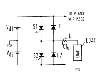
Figure 13 shows a schematic diagram of one phase (the U
phase) of a prior art PWM control inverter. Figure 13(a)
shows the main circuit of a power converter.
In Figure 13(a), Vdl, Vd2 are DC voltage sources, S1,
S2 are self-turn-off devices, D1, D2 are free-wheeling
diodes, LOAD is a load and CTU is a current detector. Also,
Figure 13(b) shows the control circuit for the power
converter. Here, Cu, C1 are comparators, GU(S) is a current
control compensation circuit, PWMC is a pulse-width
modulation control circuit, TRG is a carrier wave generator,
2114673
SM is a Schmitt circuit and GC is a gate circuit. Here,
load current Iu is detected by current detector CTU. This
is compared with a current command value IUo by comparator
Cu and a deviation ~u = IUo ~ Iu is found. This deviation
~u is amplified by current control compensation circuit
GU(S) to generate a voltage command value eu = Gu(S).~u,
which is inputted to pulse-width modulation control circuit
PWMC.
In pulse-width modulation control circuit PWMC, carrier
wave generator TRG generates a triangular wave X. This is
compared with inputted signal eu by comparator C1, and a
gate signal gu is produced via Schmitt circuit SM. Gate
circuit GC inputs this gate signal gu and produces gate
signals g1 and g2 and for self-turn-off devices S1 and S2.
The composition of this circuit explained later.
The example described above is an example for single
phase output inverters, e.g. U phase, only. In the case of
3-phase output inverters, apart from this, the V and W phase
circuits also have similar compositions.
In the following explanation, voltage command value eu
and its related values KMAX, X, Ea and Eb use normalized
values.
Figure 14 is a time chart to illustrate the operation
of PWM control circuit PWMC in Figure 13. That is to say,
When eu ' X, gu = 1 and S1 : ON (S2 : OFF)-
21146~
When eu < X, gu = and S1 : OFF (S2 ON).
At this time, when DC power source voltages Vd1, Vd2are taken as Vd1 = Vd2 = Vd/2, inverter output voltage Vu
becomes
Vu = +Vd/2, when S1 is ON (S2 is OFF); and
Vu = -Vd/2, when S1 is OFF (S2 is ON).
The mean value MVU of inverter output voltage Vu (shown
by the pecked line) becomes a value proportional to input
signal eu. Therefore, this input signal eu becomes the
inverter voltage command value.
When IUo > Iu, deviation ~u = IUo ~ Iu becomes a
positive value, and voltage command value eu increases.
Therefore, inverter output voltage Vu increases in
proportion to eu and increases load current Iu.
Conversely, when IUo < Iu, deviation ~u = I O - I
becomes a negative value and voltage command value eu
decreases. Therefore, inverter output voltage Vu decreases
and this decreases load current Iu.
Control is exercised so that, finally, Iu = IUo. When
current command value IUo is changed as sine wave form,
load current Iu also is controlled to follow this, and a
sine wave current can be supplied to load LOAD.
In this way PWM control inverters can obtain output
voltage Vu proportional to voltage command value eu. They
are therefore widely used in the driving systems of AC
motors as variable voltage variable frequency power sources.
2114679
However, prior art PWM control inverters have the
following problem.
Self-turn-off devices such as gate turn-off thyristors
(GTO) are used as devices which compose the inverter.
However, in order to protect these self-turn-off devices
(hereafter, "devices"), well-known, snubber circuits are
connected in parallel to the devices. When the device is
temporarily switched ON in order to initialize (discharge)
the capacitor of this snubber circuit, a constant-time ON
state must be maintained for the device. Also, minimum ON,
OFF times are determined by the characteristic of the device
itself, and the pulse-width of the gate signal is supplied
to satisfy this.
' MAX and -kMAX express an upper limit
value and a lower limit value of voltage command value eu.
Output voltage Vu, which is proportional to this voltage
command value eu within the limits +kMAX 2 eu 2 -kMAX can be
generated.
When eu = +kMAX~ the period of gate signal gu =
becomes ~t, and this satisfies the minimum ON time of device
S2 (the minimum OFF time of device S1). Similarly, when
eu = -kMAX, the period of gate signal gu = 1 becomes ~t, and
this satisfies the minimum ON time of device S1(the minimum
OFF time of device S2).
u MAX or eu < -kMAx~ the period of gate
2114679
signal gu = or gu = 1 becomes shorter than ~t. Therefore,
the minimum ON or OFF times of the devices cannot be
satisfied. Because of this, the voltage command value eu is
controlled to be within the limits of +kMAX ' eu 2 -kMAX by
providing a limiter circuit or the like (not illustrated).
For example, when the carrier frequency fc is taken as
fc = 500Hz, cycle T of triangular wave X becomes 2msec, and
in order to satisfy the minimum ON time (or minimum OFF
time) ~t = 200~sec, kMAX = 0.8. That is to say, in this
case the utilization factor of the inverter is 80%, and the
remaining 20% is redundant.
Therefore, a greater inverter capacity had to be
prepared for the portion by which the utilization factor was
reduced. Thus, the prior art PWM control inverter was an
uneconomic system.
SUMMARY OF THE INVENTION
Accordingly, one object of this invention is to provide
a power converter control system which executes control so
that an output voltage proportional to the input signal can
be generated, while ensuring the minimum ON time or the
minimum OFF time of the device, and thus can increase the
utilization factor of the converter, even when the absolute
value of that input signal(the voltage command value) is
great.
2114~79
Another object of this invention is to provide a power
converter control system which can reduce the voltage of the
DC power source and in which reduction in size of the power
converter, increased efficiency and cost reduction can be
achieved.
These and other objects of this invention can be
achieved by providing a control system for a pulse-width
modulation controlled power converter composed of self-turn-
off devices. The control system includes a voltage command
value generator for the power converter, a carrier wave
generator and a circuit for correcting at least one of the
voltage command value and the frequency of the carrier wave
to generate as a corrected voltage command value and a
corrected carrier wave. The control system further includes
a gate pulse signal generator for receiving a first signal
and a second signal and for comparing the first and second
signals to generate gate pulse signals to the self-turn-off
devices for controlling the power converter based on a
comparison result. The voltage command value is taken as e
(-1 < e ~ +1), and a level setting value is taken as Ea ( C
Ea < 1). The gate pulse signal generator receives the
voltage command value and the carrier wave as the first and
second signals when - Ea s e < +Ea. The gate pulse signal
generator receives one of the voltage command value and the
corrected voltage command value as the first signal and one
211~679
of the carrier wave and the corrected carrier wave as the
second signal when e ~ ~Ea or +Ea ~ e.
According to one aspect of this invention, there is
provided a control system for a pulse-width modulation
controlled power converter composed of self-turn-off
devices. The control system includes a voltage command
value generator for the power converter, a carrier wave
generator and a circuit for correcting the frequency of the
carrier wave to generate as a corrected carrier wave. The
control system further includes a gate pulse signal
generator for receiving a first signal and a second signal
and for comparing the first and second signals to generate
gate pulse signals to the self-turn-off devices for
controlling the power converter based on a comparison
result. The voltage command value is taken as e (-1 5 e s
+1), and a level setting value is taken as Ea ( < Ea < 1).
The gate pulse signal generator receives the voltage command
value and the carrier wave as the first and second signals
when ~Ea s e s +Ea. The gate pulse signal generator
receives the voltage command value as the first signal and
the corrected carrier wave as the second signal when e < ~Ea
or +Ea < e-
According to another aspect of this invention, there isprovided a control system for a pulse-width modulation
controlled power converter composed of self-turn-off
devices. The control system includes a voltage command value
2114679
generator for the power converter, a carrier wave generator
and a circuit for correcting the voltage command value to
generate as a corrected voltage command value. The control
system further includes a gate pulse signal generator for
receiving a first signal and a second signal and for
comparing the first and second signals to generate gate
pulse signals to the self-turn-off devices for controlling
the power converter based on a comparison result. The
voltage command value is taken as e (-1 s e s +1), and a
level setting value is taken as Ea ( < Ea < 1~. The gate
pulse signal generator receives the voltage command value
and the carrier wave as the first and second signals when
~Ea s e s +Ea. The gate pulse signal generator receives the
corrected voltage command value as the first signal and the
carrier wave as the second signal when e < ~Ea or +Ea < e.
These and other objects of this invention can be
further achieved by providing a control system for a pulse-
width modulation controlled power converter composed of self-
turn-off devices. The control system includes a voltage
command value generator for the power converter, a carrier
wave generator and a gate pulse signal generator for
receiving the voltage command value and the carrier wave and
for comparing the voltage command value and the carrier wave
to generate gate pulse signals based on a comparison result.
The control system further includes a correction circuit
2il4679
connected to receive the voltage command value and the gate
pulse signals for generating corrected gate pulse signals to
the self-turn-off devices for controlling the power
converter. The voltage command value is taken as e (-1 C e
< +1), and a level setting value is taken as Ea ( < Ea <
1). The correction circuit generates the gate pulse signals
as the corrected gate pulse signals as they stand, when ~Ea
e ' +Ea. The correction circuit corrects a pulse-width
(ti) of the gate pulse signals when e < ~Ea or + Ea < e,
and generates gate pulse signals with a corrected pulse-
width (ti') as the corrected gate pulse signals only when
the corrected pulse-width (ti') is equal to or larger than a
set time (ts).
The following operation can be obtained when using this
invention. Normally, voltage command value e (-1 < e < +1)
is supplied from the circuit which controls the output
current of the power converter.
When the maximum modulation factor of PWM control is
s kMAX (O < kMAX < 1), the output voltage of the
power converter is controlled by normal pulse-width
modulation control when -kMAX s e ~ +kMAX.
kMAX or +kMAX < e, the output voltage
of the power converter is controlled by adjusting the pulse
interval of the pulse with the constant width ~t which
satisfies the minimum ON time (or minimum OFF time) of the
2114679
device.
The following further operation can be obtained when
using this invention. That is to say, when the carrier wave
frequency of normal PWM control is taken as Fco, the carrier
wave frequency of the PWM control circuit is altered such
that fc fco (1 ¦e¦ )/( 1 kMAX) when e MAX MAX
< e. If a gate signal is produced by comparing this new
carrier wave (triangular wave) and voltage command value e,
a pulse with an almost constant width at can be obtained.
Moreover, since frequency fc reduces as the absolute value
¦e¦ of voltage command value e approaches, 1, a voltage
proportional to voltage command value e can be obtained for
the output voltage of the power converter even when voltage
command value e is within the region of e < -kMAX or +kMAX <
e.
In this way, when using the power converter control
system of this invention, a voltage proportional to voltage
command value e is obtained for the output voltage of the
power converter even when voltage command value e is within
the region of e < -kMAx or +kMAX < e. Moreover, a pulse
with a constant width at which satisfies the minimum ON time
(or minimum OFF time) of the device can be obtained.
Therefore it is possible to increase the utilization factor
of the power converter to 100%, and the prior art problem
can be solved.
That is to say, it is possible to continue to obtain
-- 10 --
21~4679
output voltage Vu proportional to voltage command value eu
even in the region where the absolute value of the voltage
command value eu is greater than the maximum modulation
factor kMAX of the PWM control. In addition, it is possible
to satisfy the minimum ON time or the minimum OFF time of
the devices which compose the converter. As a result, in
the case of PWM control of a power converter such as an
inverter or a converter, it is possible greatly to increase
the utilization factor of that converter. Also, it is
possible to reduce the voltage Vd of the DC power source by
that amount. Thus, it becomes possible to achieve reduction
in size, increased efficiency and cost-reduction of the
converter.
When using this invention, the following still further
operation can be obtained. That is to say, it is possible
to generate voltage Vu from the converter proportional to
voltage command value eu mean value-wise, while selecting
either the generation of a pulse which satisfies the minimum
ON time (or minimum OFF time) ~t of the device or the
elimination of generating that pulse, when the original
voltage command value eu is within the regions eu < ~Ea or
eu > +Ea. As a result, it becomes possible to increase the
utilization factor of the converter up to 100%.
When using this invention, the following yet further
operation can be obtained. That is to say, when voltage
-- 11 --
2114679
command value e is -kMAX s e s +kMAX, the output voltage of
the power converter is controlled by normal pulse-width
modulation control. Also, when e < -kMAX or +kMAX < e, a
pulse-width ~ti' = ti + ~ti of a new control pulse is
obtained by adding an error time ~ti to a width ti of a
control pulse Pi. This pulse-width ti' is compared with a
set time ts. When ti' 2 ts, the output pulse is outputted
and, at the same time, ~ti = O is stored in the memory.
When ti' < ts, ~t = ti' is stored in the memory without
outputting the output pulse. Then, error time ~ti is
controlled so that it lS reflected in the following control
pulse. As a result, it is possible to obtain an output
voltage which is proportional to the voltage command value
e. Moreover, it is possible to satisfly the minimum OFF
time (or minimum ON time) of the device. Therefore, it
becomes possible to increase the utilization factor of the
converter to 100% and thus to solve the prior art problem.
BRIEF DESCRIPTION OF THE DRAWINGS
A more complete appreciation of the invention and many
of the attendant advantages thereof will be readily obtained
as the same becomes better understood by reference to the
following detailed description when considered in connection
with the accompanying drawings, wherein:
Figure 1 is a schematic diagram of the main circuit and
- 12 -
21141~79
the control circuit showing an embodiment of a power
converter control system of this invention;
Figure 2 is a characteristic graph to illustrate the
operation of the control system in Figure 1;
Figure 3 is a time chart to illustrate the operation of
the system in Figure 1;
Figure 4 is a block diagram of the gate circuit GC of
the system in Figure 1;
Figure 5 is a time chart to illustrate the operation of
the gate circuit GC in Figure 4;
Figure 6 is a schematic diagram of the main circuit and
the control circuit showing another embodiment of a power
converter control system of this invention;
Figure 7 is a characteristic graph to illustrate the
control operation of the system in Figure 6;
Figure 8 is a time chart to illustrate the control
operation in Figure 6;
Figure 9 is a control block diagram showing a further
embodiment of the power converter control system of this
invention;
Figure 10 is a flow-chart to illustrate the operating
process of Figure 9;
Figure 11 is a diagram to illustrate PWM control
operation in Figure 9 when the voltage command value is
positive;
Figure 12 is a diagram to illustrate PWM control
211~679
operation in Figure 9 when the voltage command value is
negative;
Figure 13 is a schematic diagram of the main circuit
and the control circuit to illustrate a prior art power
converter control system; and
Figure 14 is a time chart to illustrate the prior art
control system in Figure 13.
DETAILED DESCRIPTION OF THE PREFERRED EMBODIMENTS
Referring now to the drawings, wherein like reference
numerals designate identical or corresponding parts
throughout the several views, the embodiments of this
invention will be described below.
Figure 1 shows an embodiment of a power converter
control system of this invention. Figure l(a) is a
schematic diagram of the main circuit, and Figure l(b) is a
block diagram of the control circuit.
In Figure l(a), Vd1, Vd2 are DC voltage sources, S1, S2
are self-turn-off devices D1, D2 are free-wheeling diodes,
LOAD is load and CTU is current detector. The composition
of this main circuit is the same as that in Figure 13(a).
As shown in Figure l(b), comparator Cu, current control
compensation circuit GU(S), a function generator FX, a
voltage/frequency converter V/f, triangular wave generator
TRG and a pulse-width modulation control circuit (PWM
- 14 -
211~679
control circuit) PWMCA are provided as the control circuit.
PWM control circuit PWMCA is composed of comparator C1,
Schmitt circuit SM and gate circuit GC.
This drawing only shows the portion for one phase (e.g.
the U phase). In the case of a 3-phase load, the portions
for the other two phases (V and W phases) are composed in
the same way.
U-phase load current Iu is detected by current detector
CTU, and is inputted to comparator Cu of the current control
circuit. Comparator Cu compares current command value IUo
and current detection value Iu, and finds the deviation
~u = IUo - Iu. This deviation ~u is amplified by the
following control compensation circuit GU(S) to generate
voltage command value eu.
This voltage command value eu is inputted to PWM
control circuit PWMCA and, at the same time, is inputted to
function generator FX.
Figure 2 shows a practical example of the input/output
characteristics of function generator FX. That is to say,
when the absolute value of input signal eu is at or below a
certain level setting value Ea ( s Ea ~ 1), the output
signal is taken as eO = Eo = constant. When the absolute
value of input signal eu is greater than Ea, the output
signal is taken as eO = Eo.(1 - ¦eU¦)/(1 - Ea).
Output signal eO of function generator FX is inputted
to the following voltage/frequency converter V/f, and is
21~4679
converted by voltage/frequency conversion to a clock signal
of frequency fCL proportional to eO. This clock signal is
inputted to the following triangular wave generator TRG and
determines the carrier wave frequency fc of PWM control.
That is to say, frequency fc f triangular wave X
becomes constant at fc = fco when the absolute value of
voltage command value eu is ¦eUI ~ Ea, and becomes fc =
fCo.(1 - ¦eul)/(l - Ea) when ¦eU¦ > Ea-
When the maximum modulation factor of PWM control istaken as kMAX and it is set that Ea = kMAX, frequency fc f
triangular wave X becomes constant (fc = fco) when ¦e
k and becomes fc = fco.(l leul) MAX
MAX-
Figure 3 shows an example of the PWM control operation
of the system in Figure 1. In the drawing, eu is voltage
command value, X is carrier wave (triangular wave) signal,
+kMAX and -kMAX shown by the pecked lines are the maximum
modulation factors of prior art PWM control, gu is the
signal, and Vu is inverter output voltage.
The following is a description of the case when Ea =
k is set. When -kMAX ' eu ~ +kMAX'
control carrier wave becomes constant (fc = fco) and normal
pulse-width modulation control is executed. In PWM control,
voltage command value eu and triangular wave X are compared,
and gate signal gu of devices S1 and S2 produced. That is
to say,
- 16 -
2114679
when eu ' X~ gu = 1 and S1 : ON (S2 OFF); and
when eu < X, gu = and S2 : ON (S1 OFF).
When the DC source voltage Vd1, Vd2 are taken as Vd1
Vd2 = Vd/2, the output voltage Vu of the inverter becomes
Vu = +Vd/2, when S1 is ON (S2 is OFF); and
Vù = -Vd/2, when S2 is ON (S1 is OFF).
Mean value MVU of inverter output voltage Vu becomes a
value proportional to voltage command value eu. In this
case the "1" and "O" periods of gate signal gu always
becomes longer than the minimum ON time (or minimum OFF
time) ~t of devices S1 and S2 which compose the inverter.
Thus there is no problem of any kind.
Next, the operation when eu > +kMAX is described with
reference to Figure 3. In the region of eu > +kMAX, PWM
control carrier wave frequency fc is obtained by fc = f cO-
(1 - eu)/(l - kMAX). When gate signal gu is produced by
comparing this carrier wave (triangular wave) X and voltage
command value eu,
when eu 2 X, gu = 1 and S1 : ON (S2 : OFF); and
when eu < X, gu = and S2 : ON (S1 : OFF).
Thus, mean value MVU of inverter output voltage Vu
becomes a value proportional to voltage command value eu in
the same way as in normal PWM control. When taking the
cycle of triangular wave X as Tc = l/fc and the period of
gate signal gu = as ~t, mean value MVU of inverter output
211~679
voltage Vu is
u (Vd/2).(Tc - 2.~t)/T .
Since this is proportional to voltage command value eu,
the relationship
eu = (Tc ~ 2.~t)/TC
is established, and therefore
~ t = Tc(l - eU)/2
= (1 - eu)/(2 fc)
u)(1 kMAX)/{2.fCo(l - e )}
= (1 - kMAx)/(2 fco)
Thus period ~t becomes a constant value regardless of
the size of voltage command value eu.
In this way, mean value MVU of inverter output voltage
Vu can be obtained as a value proportional to voltage
command value eu even in the region of eu > +kMAX. Also,
the minimum ON time (minimum OFF time) ~t of devices S1 and
S2 which compose the inverter can be satisfied.
In the same way also, when eu < -kMAX' mean value MVu
of inverter output voltage Vu becomes a value proportional
to voltage command value eu. Also, the period ~t of gate
signal gu = 1 becomes constant, and the minimum ON time
(minimum OFF time) of devices S1 and S2 which compose the
inverter can be satisfied.
In the actual system, when carrier wave frequency fc is
changed following voltage command value eu, an operation
error is generated, and also there is sometimes a problem
- 18 -
21 1 4679
with the accuracy of triangular wave X. As a result, when
eu > +kMAX, the period when the gate signal gu should become
gu = (or when eu < -kMAX, the period when the gate signal
gu should become gu = 1) does not become accurately equal to
~t. In this case, it is allowable for inverter output
voltage Vu to be controlled with a certain degree of error
in relation to voltage command value eu. However, if the
minimum ON time (or minimum OFF time) ~t of devices S1 and
S2 cannot be satisfied, there will be a risk of the devices
S1 and S2 being damaged. Therefore, gate signal gu should
be processed by gate circuit GC so that the minimum ON time
(or minimum OFF time) of the devices are satisfied whatever
the case may be.
Figure 4 shows gate circuit GC of the system in Figure
1. In the drawing, IN is an inversion circuit, MMA1 to MMA3
and MMB1 to MMB3 are monomulti circuits, AND1 and AND2 are
AND circuits and OR1 and OR2 are OR circuits.
Also, Figure 5 shows a time chart to illustrate the
operation of Figure 4.
In Figure 5,
gu is a gate signal;
Igu is an inversion signal of gate signal gu obtained
via inversion circuit IN;
m1a is an output signal of monomulti MMA1 which
operates at the falling of gate signal gu;
-- 19 --
2114~79
m2a is an output signal of monomulti MMA2 which
operates at the falling of gate signal gu;
m3a is an output signal of monomulti-MMA3 which
operates at the falling of output signal m2a;
m1b is an output signal of monomulti MMB1 which
operates at the falling of inversion signal Igu;
m2b is an output signal of monomulti MMB2 which
operates at the falling of inversion signal Igu;
m3b is an output signal of monomulti MMB3 which
operates at the falling of output signal m2b; and
g1 and g2 are gate signals of devices S1 and S2.
Monomulti circuits MMA2 and MMB3 supply dead times tD
for preventing inverter devices S1 and S2 switching ON
simultaneously. Also, monomulti circuits MMA1 and MMB1
supply minimum OFF times toFF for the devices, and monomulti
circuits MMA3 and MMB3 supply minimum ON times toN for the
devices. These have the relationship toN = toFF - 2.tD.
Gate signals g1 and g2 are obtained by executing the
following logic operations following the circuit in Figure
4. Here, Im2a is taken as an inversion value of signal m2a
and Im2b as an inversion value of signal m2b.
gu X mla X Im2b + m3b
g2 = Igu x mlb x Im2a + m3a
When gate signal g1 is "1", device S1 is ON, and when
it is "O", S1 is OFF. Also, when gate signal g2 is "1",
- 20 -
211~679
device S2 is ON, and when it is "O", device S2 is OFF. There
is a dead time tD when devices S1 and S2 are shifting
between ON and OFF respectively, and this prevents devices
S1 and S2 being ON simultaneously.
Monomulti circuits MMA1 and MMA2 operate when signal gu
shifts from "1" to "O". However, when signal m1b is O, it
provides an interlock so that they do not operate.
Similarly, monomulti circuits MMB1 and MMB2 operate when
inversion signal Igu shifts from "1" to "O". However, when
signal m1a is O, it provides an interlock so that they do
not operate.
First, the case when period ~t1 of gu = has become
shorter than minimum OFF time toFF is described. Monomulti
circuits MMA1 and MMA2 operate through the falling of signal
gu. Signal m1a becomes "O" only during time toFF, and
signal m2a becomes "1" only during time tD. Also, monomulti
circuit MMA3 operates at the falling of signal m2a. Signal
m3a becomes "1" only during time toN. Inversion signal Igu
falls at time ~t1 after the fall of signal gu. However,
since signal m1a has already become "O", MMB1, MMB2 and MMB3
will not operate. Gate signal g1 of device S1 is obtained
by the logic operation described above, and becomes "O" only
during time toFF from the point of the falling of gate
signal gu, and this satisfies the minimum OFF time of device
S1. Also, gate signal g2 of device S2 becomes "1" delayed
- 21 -
211~679
only by time tD from the point of the falling of signal gu,
and device S2 is caused to be ON only during time toN.
Therefore, this satisfies the minimum ON time of device S2.
Next, the case when period ~t2 of signal gu = 1 has
become shorter than minimum OFF time toFF is described.
Monomulti circuits MMB1 and MMB2 operate through the falling
of inversion signal Igu. Signal m1b becomes "O" only during
time toFF, and signal m2b becomes "1" only during time tD.
Also, monomulti circuit MMB3 operate at the falling of
signal m2b. Thus signal m3b becomes "1" only during time
toN. Signal gu falls at time ~t2 after the fall of
inversion signal Igu. However, since signal m1b has already
become "O", MMA1, MMA2 and MMA3 will not operate. As a
result, gate signal g2 of device S2 becomes "O" only during
the time toFF from the point of the falling of inversion
signal Igu, and this satisfies the minimum OFF time of
device S2. Also, gate signal g1 of device S1 becomes "1"
delayed only by time tD from the point of the falling of
inversion signal Igu, and device S1 is caused to be ON only
during time toN. Therefore, this satisfies the minimum ON
time of device S1.
In this gate circuit, when the period in which gate
signal gu becomes "1" or "O" becomes longer than minimum OFF
time toFF, gate signals g1 and g2 are outputted as they
stand by taking only dead time tD into consideration. That
- 22 -
2114679
it to say, at point p in Figure 5, signal gu falls and
monomulti circuits MMA1 to MMA3 operate. However, since the
period in which gu = after point P is longer than time
toFF, gate signal g1 becomes the same as gate signal gu.
Also, gate signal g2 is delayed by dead time tD by signal
m2a of monomulti circuit MMA2 and becomes g2 = 1.
In this way, even if the pulse-width of gate signal
becomes narrower than the minimum ON time or minimum OFF
time of the device due to operational error in PWM control,
this is adjusted by gate circuit GC so that the device will
not be damaged. In this case, a slight error may be
included in the proportional relationship between voltage
command value eu and the mean value of inverter output
voltage Vu, but this will not create any problem in
practical use.
When using the power converter control system in the
above embodiment, output voltage Vu of inverter proportional
to voltage command value eu can be continuously obtained
even in the region where the absolute value of voltage
command value eu is greater than the maximum modulation
factor kMAX of the PWM control. Also, it is possible to
satisfy the minimum ON time or minimum OFF time of the
devices which compose the converter. As a result, when
exercising PWM control of power converters such as inverters
or converters, the utilization factor of the converter can
- 23 -
2114679
be greatly increased. Thus, reduction in the voltage Vd of
the DC power becomes possible. Therefore reduction in size
of the converter, increased efficiency and cost-reduction
can be achieved.
Figure 6 shows another embodiment of the power
converter control system of this invention. Figure 6(a) is
a schematic diagram of the main circuit, and Figure 6(b) is
a block diagram of its control circuit.
In Figure 6(a), Vd1, Vd2 are DC voltage sources, S1, S2
are self-turn-off devices, D1, D2 are free-wheeling diodes,
LOAD is load and CTU is current detector. The composition
of this main circuit is the same as that in Figure l(a).
However, the composition of the control circuit in Figure
6(b) differs. That is to say the control circuit shown in
Figure 6(b) is composed of comparator Cu, current control
compensation circuit GU(S), an adder A1, a subtractor A2,
sample hold circuits SH1, SH2, a signal correction circuit
SX, pulse-width modulation control circuit (PWM control
circuit) PWMC and gate circuit GC. This drawing shows only
the portion for one phase (e.g. the U phase). In the case
of a 3-phase load, the portions for the other two phases (V
and W phases) are composed in the same way.
U-phase load current Iu is detected by current detector
CTU, and is inputted to comparator Cu of the current control
- 24 -
2114679
circuit. Comparator Cu compares current command value IUo
and current detection value Iu, and finds the deviation ~u =
IUo - Iu. This deviation ~u is amplified by the following
control compensation circuit GU(S) to generate an original
voltage command value eu. This original voltage command
value eu is inputted to adder A1 and added to an error
signal ~e which is held by second sample hold circuit SH2.
First sample hold circuit SH1 takes in an output signal
e1 = eu + ~e of adder A1 in synchronization with the PWM
control carrier wave signal X from PWM control circuit PWMC,
and holds that value. Output signal e1 of that sample hold
circuit SH1 is inputted to the following signal correction
circuit SX, and is converted to a new voltage command value
e2 depending on its size.
Figure 7 shows a practical example of the input/output
characteristics of signal correction circuit SX. The input
is output signal e1 from sample hold circuit SH1. New
voltage command value e2 is outputted by comparing signal e
and level setting values Ea and Eb ( ' Ea ~ Eb ~ 1) such
that
when -Eb 2 e1, e2 = -1
when -Eb < e1 < a' e = -E
when ~Ea ' e1 - +Ea' e2 = el
when +Ea < e1 < Eb' e2 = +E
when +Eb ' e1' e2 = +1.
- 25 -
2114679
This voltage command value e2 is inputted to PWM
control circuit PWMC in Figure 6. Gate circuit GC receives
output gate signal gu of PWM control circuit PWMC, and
outputs gate signals g1 and g2 for self-turn-off devices S
and S2. The circuit compositions of PWM control circuit
PWMC and gate circuit GC are respectively the same as those
in Figure 13(b) and Figure 4.
The level setting values Ea and Eb of signal correction
circuit SX are determined taking account of the minimum ON
times At of the devices. For instance, when taking the
maximum value EmaX of the carrier wave signal as E = 1
and the carrier frequency as fc,
1 - Ea = ~t fc Emax
1 - Eb = (1 - Ea)/2
are selected.
That is to say, level setting values Ea and Eb are
selected so that when the input signal (new voltage command
value e2 of PWM control circuit PWMC is e2 = Ea~ the period
of gate signal gu = which is supplied to the device
becomes ~t. When taking ~t = 200~sec, fc = 500Hz, level
setting values Ea and Eb become Ea = 0.8 and Eb = 0'9'
Also, in this case, level setting value Ea is set equal to
the maximum modulation factor KMAX OF PWM control-
Returning to Figure 6, subtractor A2 computes thedifference between the input and output signals of signal
correction circuit SX. This is taken as error signal ~e =
- 26 -
2114679
e1 - e2 and is inputted to second sample hold circuit SH2.
Second sample hold circuit SH2 operates in synchronization
with PWM control carrier wave signal X from PWM control
circuit PWMC, however it operates by shifting its timing
slightly from the operation of first sample hold circuit
SHl .
In the case of the absolute value of original voltage
command value eu being small, that is to say when ~Ea s e1 s
Ea new voltage command value e2 becomes e2 = e1, and the
power converter is PWM controlled in the same way as in
prior art. Also, the error signal ~e becomes zero and the
output of second hold circuit SH2 also becomes zero.
The case of the absolute value of the PWM control input
signal (voltage command value) eu having become great, that
is to say the operation when eu < ~Ea or eu > +Ea~ is as
follows. This operation is described with reference to
Figure 8, taking as an example the case when Ea = 0.8, Eb =
0.9 and voltage command value eu = +0.85 = constant.
In Figure 8, eu shows original voltage command value, X
is PWM control carrier wave signal, e2 is new PWM control
input signal, SP1 and SP2 are timing signals for sample hold
circuits SH1 and SH2 when eu > , SP1 2
signals for sample hold circuits SH1 and SH2 when eu < ~ gu
is gate signal and Vu is inverter output voltage.
Since eu > , sample hold circuits SH1 and SH2 operate
211~679
with timing signals SP1 and SP2.
First, first sample hold circuit SH1 is operated in
synchronization with PWM control carrier wave signal
(carrier signal) X, and takes in the sum of original voltage
command value eu and error signal ~e held in second sample
hold circuit SH2. First of all, when taking ~e = O at time
to, the addition value e1 becomes e1 = eu + ~e = +0.85.
Therefore, since +Ea < e1 < Eb, the output e2 of signal
correction circuit SX becomes e2 = +E and is inputted to PWM
control circuit PWMC.
In PWM control circuit PWMC, the signal e2 = +Ea and
carrier wave signal X are compared, and a gate signal with a
pulse-width in which the period of gate signal gu =
satisfies the minimum ON time ~t is transmitted to the power
converter. The power converter generates voltage Vu which
is proportional to value +Ea = +0.8. This means that
voltage Vu is outputted which is smaller by a portion
proportional to e1 - Ea = 0-05 Sample hold circuit SH2 is
also operated in synchronization with carrier wave signal X,
but it is operated delayed by a time td from sample hold
circuit SH1. Therefore, ~e = e1 - Ea = 0 05 is held as the
error signal. This error signal ~e is once again added to
voltage command value eu = +0.85. Thus, signal e1 =eu + ~e
= 0.9 is inputted to signal correction circuit SX by the
next operation of first sample hold circuit SH1 at time t1.
- 28 -
211~679
Therefore, this time, signal e1 becomes +Ea ~ e1 ~ 1,
and e2 = 1 is inputted to PWM control circuit PWMC. At e2 =
1, there will be no period of gate signal gu = and the
output voltage Vu of the power converter will be maximum
Therefore this means that more voltage is outputted as
voltage Vu by a portion proportional to 1 ~ eu = 0.15 than
in the case when original voltage command value eu is used
as it stands. Since a smaller voltage was outputted under
the previous control by a portion proportional to eu ~ Ea =
0.05, in total voltage Vu will become greater by a portion
proportional to 0.15 - 0.05 = 0.1. At this time, error
signal ~e becomes ~e = e1 - e2 = -0.1 and is held in sample
hold circuit SH2.
Furthermore, when signal eu = +0.85 is inputted at time
t2, the above error signal ~e = -0.1 is added, and signal e
= eu + ~e = 0.75 is inputted to signal correction circuit
SX. Therefore, signal e1 becomes e1 < +Ea and voltage
command value e2 = e1 = 0.75 is supplied to the PWM control
circuit PWMC. Therefore this means that voltage Vu is
outputted which is smaller by a portion proportional to eu ~
e2 = 0.1 than in the case when original voltage command
value eu = 0.85 is used at it stands. Since a greater
voltage was outputted as voltage Vu under the previous
control by a portion proportional to 0.1, in total the error
will be zero. At this time, the error signal ~e becomes
- 29 -
211~679
~e = e1 - e2 = ~ and this is held in second sample hold
circuit SH2. That is to say, second sample hold circuit SH2
holds the latest total error voltage (accumulated value).
This error signal ~e is corrected every one cycle of PWM
control carrier wave X so that its absolute value never
becomes greater than (1 - Eb) = O.1. Therefore, as long as
voltage command value eu does not change suddenly, the mean
value MVU of converter output voltage Vu becomes a value
proportional to original voltage command value eu.
When original voltage command value eu has become eu < ~
Ea, sample hold circuit SH1 operates by timing signal SP1'
at times tol, t1', t2'. Sample hold circuit SH2 operates by
timing signal SP2' at times delayed by time td~
respectively. Thus, while period of gate signal gu = 1
satisfies the minimum ON time (or minimum OFF time) ~t,
converter output voltage Vu becomes a value proportional to
voltage command value eu.
In this way, when using this embodiment of the power
converter control system of this invention in Figure 6, if
original voltage command value eu enters the region f eu < ~
Ea or eu > +Ea~ a voltage Vu proportional to voltage command
value eu can be generated from the converter mean value-wise
while selecting either the generation of a pulse which
satisfies the minimum ON time (or minimum OFF time) ~t of
the device, or the elimination of the pulse. As a result,
the utilization factor of the converter can be increased to
- 30 -
2114679
100%.
Here, the description has been given taking Eb = 0'9
However, similar results can be achieved in the region of Ea
< Eb ~ 1.
Carrier wave frequency fc of PWM control circuit PWMC
in the embodiment in Figure 6 differs from that in the
embodiment in Figure 1, and is constant. However, the two
embodiments have a common point in that, in the case of the
absolute value of original voltage command value eu becoming
greater than a certain level of setting value Ea, output
voltage Vu of the converter can be generated proportional to
voltage command value eu at a constant pulse-width ~t such
that the period of gate signal gu = (or the period of gate
signals gu = 1) satisfies the minimum ON time (or minimum
OFF time) of the device and by adjusting the interval of
that pulse, in other words, by adjusting the pulse density.
Next, a further embodiment of this invention is
described with reference to the drawings. Figure 9 shows
part, that is to say the U-phase only, of the power
converter control system of the PWM control of this
invention.
In Figure 9,
Ga is a discrimination circuit which outputs a
discrimination signal Sk(=1) when voltage command value eu
is positive and a discrimination signal Sk(=O) when it is
- 31 -
2114679
negative;
SW1 and SW2 are switches which operate in response to
the output signals of discrimination circuit Ga;
CAL is a calculation circuit which has a memory which
stores an error time ~ti when a pulse width ti of a control
pulse Pi is narrower than a set time ts, as described later;
TCONT is a pulse circult which outputs pulse Ps of a
width of set time ts; and
INV1 and INV2 are inversion circuits.
In the case of a 3-phase load, the portions for the
other two phases (V and W phases) are composed in the same
way.
The following is a description of the control
operation. This is for the case of voltage command value eu
being positive and discrimination signal Sk being Sk = 1.
In Figure 9, control pulse Pi(gu), which is obtained by
the comparison of voltage command value eu and triangular
wave X from carrier wave generator TRG, is inputted to a
terminal b of switch SW1 and to inversion circuit INV1.
Voltage command value eu is inputted to discrimination
circuit Ga. Also, an output signal IPi of inversion circuit
INV1 is inputted to a terminal c of switch SW1, and output
signal Sk of discrimination circuit Ga is inputted to
switches SW1 and SW2.
Next, in switch SW1, terminal b is connected to a
terminal a when discrimination signal Sk = 1, and output Pi
- 32 -
2114679
applied to terminal b is inputted to calculation circuit CAL
and pulse circuit TCONT. Pulse circuit TCONT outputs pulse
Ps in synchronization with input pulse Pi to calculation
circuit CAL. Calculation circuit CAL executes a logic
operation using inputted pulses Pi and Ps, and outputs pulse
Po. This is inputted to a terminal e of switch SW2 and to
inversion circuit INV2. Output pulse IPo of inversion
circuit INV2 is inputted to a terminal f of switch SWZ. In
switch SW2, terminal e is connected to a terminal d when
discrimination signal Sk = 1, and terminal d outputs gate
signal gu'. Gate circuit GC receives gate signal gu' and
outputs gate signal g1 and g2 for self-turn-off devices S
and S2.
In the case of signal Sk = O, terminals c and a are
connected in switch SW1, terminals f and d are connected in
switch SW2, and signals IPi and IPo are used for the
control. Figure 10 shows an operation flow-chart for
calculation circuit CAL. This describes the case of voltage
command value eu is eu > - In the flow-chart, ti is the
pulse-width of input pulse Pi selected by switch SW1, and ts
shows the width of pulse Ps for time-setting. Calculation
circuit CAL measures the pulse-width ti and ts of the
initially inputted pulses Pi and Ps using commonly-known
methods.
Next, when pulse-width ti is inputted, error time ~ti
which is stored in a memory (not illustrated) is added to
211~79
it, and that addition value ti' = ti + ~ti is inputted to a
comparator.
In the comparator,
when ti' > ts, control pulse Po of pulse-width ti' is
outputted as it stands, and error time ~ti = O is stored in
the memory; and
when ti' < ts, error time ~ti = ti' is stored in the
memory without outputting pulse Po. That is to say, the
calculation is executed so that a new control pulse is
generated by adding that error time ati to the following
control pulse.
Next, the PWM control operation waveforms of this
embodiment are shown.
Figure 11 is the case when voltage command value eu is
positive and discrimination signal Sk is Sk = 1.
In the drawing, tin is the pulse-width of control pulse
Pi obtained by the comparison of voltage command value eu
and triangular wave X, and ts shows the set time (-toff ;
minimum OFF time of the device), where n is the number of
the input pulse.
Firstly, error time ~ti is set to ~ti = O (initial
value), and when pulse-width ti1 of first control pulse Pi
is inputted, pulse-width ti1 is adjusted to new pulse-width
ti1' = ti1 + ~ti. However, since error time ~ti is ~ti = O,
pulse-width ti', becomes ti1' = ti1 and ti1'< ts. Therefore
control pulse Po is not outputted.
- 34 -
211Ç679
As a result, error time ~ti becomes ~ti = ti1' (=ti1),
and this is stored in the memory.
Next, when pulse-width ti2 of second control pulse Pi
is inputted, pulse-width ti2 is adjusted to ti2'= ti2 +~ti.
As a result, pulse-width ti2' becomes ti2' = ti2 + ti and
ti2 ' 2 ts. Therefore pulse Po of control pulse-width ti1'
is outputted. Therefore, error time ~ti becomes ~ti = O,
and this is stored in the memory.
When pulse-width ti3 of third control pulse Pi is
inputted, pulse-width ti3', which has been adjusted in the
same way as in the case of the first pulse becomes ti3'
(=ti3) < ts, and control pulse Po is not outputted. Thus
error time ~ti becomes ~ti = ti3' = ti3, and this is stored
in the memory. When pulse-width ti4 of fourth control pulse
Pi is inputted, pulse-width ti4 is adjusted to ti4'= ti4 +
~ti = ti4 + ti3. However, since ti4' < ts, no control pulse
Po is outputted. As a result, the new error time ~ti
becomes ~ti = ti4' = ti4 + ti3, and this is stored in the
memory.
Pulse-width ti5 of fifth control pulse Pi is wider than
set time ts. However, pulse-width ti5 is adjusted to ti5' =
ti5 + ~ti (=ti5 + ti4 + ti3). As a result, ti5' ~ ts, and
control pulse Po is outputted , and error time ~ti becomes
~ti = O. As a result, output pulse Po is inputted as it
stands from terminal d to gate circuit GC as gate signal
- 35 -
21 1 4B79
gU
Figure 12 shows the case when voltage command value eu
is negative and discrimination signal Sk is Sk = O.
Input pulse Pi is inverted by inversion circuit INV1
and is inputted to calculation circuit CAL as inverted pulse
IPi, and calculation is executed in the same way as in
Figure 10. In this case, pulse-width ti should be read as
the pulse-width of inverted pulse IPi in Figure 10. The
output pulse Po of calculation circuit CAL is inverted by
inversion circuit INV2 and becomes inverted pulse IPo. This
is inputted to gate circuit GC from terminal d as gate
signal gu'.
As described above, pulse-width ti' of adjusted control
pulse Pi and the set time ts are compared. When ti' ' ts, a
control pulse Po of pulse-width ti' is outputted as it
stands. When ti' < ts, control pulse Po is not outputted,
but error time ~ti = ti' is stored in the memory. By
reflecting that error time ~ti in the following control
pulse, an output voltage proportional to voltage command
value eu is obtained. Thus, the utilization factor of the
power converter can be increased.
The above is a description for the U phase of the power
converter. However, the same effect can be achieved for the
V phase and the W phase. Needless to say, the same effect
can be achieved in the case of a 3-phase 3-wire load.
Also, the above embodiments have been described for an
- 36 -
211~679
inverter which converts DC power to AC power. Needless to
say this invention can be applied in the same way for a
converter which converts AC power to DC power.
When using the power converter control system of this
invention, it is possible continuously to obtain output
voltage of the power converter proportional to voltage
command value, even if the absolute value of the voltage
command value is in the region where it is greater than the
maximum modulation factor of PWM control. Also, it is
possible to satisfy the minimum ON time or minimum OFF time
of the devices which compose the power converter.
Also, when using the power converter control system of
thus invention, output voltage of the power converter can
continuously be obtained proportional to voltage command
value, by adding error time to pulse-width of control pulse;
finding new control pulse-width; comparing this new pulse-
width with set time and outputting a control pulse in
response to that result, even if the absolute value of the
voltage command value is in the region where it is greater
than the maximum modulation factor of PWM control. Also, it
is possible to satisfy the minimum ON time or minimum OFF
time of the devices which compose the converter.
As a result, in the case of PWM control of power
converters such as inverters or converters, it is possible
greatly to increase the utilization factor of those
- 37 -
2114679
converters. Thus it is possible to reduce voltage of the
direct current power source by that amount. Therefore
reduction in size of the power converter, increased
efficiency and cost-reduction can be achieved.
Obviously, numerous modifications and-variations of the
present invention are possible in light of the above
teachings. It is therefore to be understood that within the
scope of the appended claims, the invention may be practiced
otherwise than as specifically described herein.
- 38 -