Note: Descriptions are shown in the official language in which they were submitted.
~E~T T~Al~J ~ ON
SPECIFICATION
DEVIC~ FOR AND METHOD OF COUNTING BIT E~RORS AND
DEVICE FOR ~ND METHOD OF IDENTIFYING SIGN~S
TECHNICAL FIELD
The present invention relates to a device for and a
method of counting the number of bit errors in a recep~ion
signal in digital communication~ and, more particularly,
relates to a device for and a method of identifying
whether a reception signal is a speech signal or a control
signal and outputting an identification siynal/ a decoded
signal, and the number of bit errors counted.
.
BACKGROUND ~R~
For T~MA digital mobile communication, a tran~mlssion
sys~em is used which transmits di~ferent signals such as a
speech signal ~nd a F~CCH (Fast Associated Control
Channel) signal, which is a kind of a con~rol signal with
use o~ the same data region of a channel. These two kinds
of the signals axe the same i.n the numbers of to~al bits,
but different from one another in the method of error
correction or error detection. The ~peech sign~l or the
~CCH signal is transmitted from a transmission side in
accordance with the cond.it.ions of the use thereof.
2 2~3~
Howevex, a flag is not transmitted to identify whether a
transmission signal is the speech signal or the FACCH
signalO A reception side is accordingly needed to judge
whether a transmitted signal is the speech signal or the
FACCH signal.
The following describes the configuration of a prior ~~
art signal identifier device.
The prior art signal identifier device comprises an
error correcting/decoding part for processing speech
signal, an error detecting/decoding part for processing
speech signals, an error correcting/decoding part for
control signals, and an error detecting/decoding part for
control signals. The erxor correcting/decoding part for
speech signals employs a decoding method for error
correction codes used in encoding part or all of the
speech signals at the transmission side. ~he error
correctiny/decoding paxt for control signals employs a
decoding method for an error correction codes used in
encoding part or all of con~rol signals on the
transmission side. The error detecting/decoding part for
speech ~ignals or for control signals uses a de~ection
method corresponding to respective error detection codes
applied at the transmission side.
In the following, there will be described the
operation of the prior art signal identifier device. A
transmission signal from the transmussion side is first
received. The received transmission signal is entered
into the error correcting/decoding part for processing
speech signals and into the error correcting~decoding part
for processing control signals. The recep~ion signal
entered is decoded in response to the decoding methods of
the respec~ive error correcting/decoding parts, and is
outputted as decoded signals. The decoded output signals
are entered into the ~rror detection decoder parts. On
the basis of the error detection code applied at the
transmission side, it is inspected whether or not each
decoded signal contains partly or wholly any bit errors,
and a correct/false ~ignal is generated. The signal
identifier device herein receives the decoded signals and
the correcttfalse signals and compares error~ in the
correct/false signals and regards, as the transmitted
signal, the correct/false signal in which no exror is
detected and outputs the decoded signal and the
identification signal of that signal.
Although there is found no adequate reference for the
signal identifying system a detailed description for the
error detection code can be found in "Encoding Theory"
written by Hiroshi Miyagawa, Yoshiro Iwadare, and Hideki
Imai, published by (joint-stock company) Shokodo Co.,Ltd.
A set of two devices, each of which has been disclosed in
"Japanese Laid-Open Patent Publication (A) No.60-144038
titled as A Digital Signal Transmission System, Matsushita
Electric Industry (Co.,Ltd.), Keishi Matsuya" are
applicable to the signal identifier device.
The following describes a bit error counter device in
transmitter/receiver equipment for use in digital
communication. A digital communication system is recently -
proposed, in which an original signal is rendered to
convolution encoding at the transmission side and is then
transmitted to the reception side as a transmission
signal, and further at the reception side a reception
signal is Viterbi-decoded. The transmission system
enables -the number of bit errors to be counted ~rom a main
signal itself such as a speech signal and an image signal
without transmitting a known signal from the transmission
side to the reception side, thereby a receiver can
determine the transmission quality of a transmission
channel based on the number of bit errors counted.
The following describes a prior ar~ bit error counter
device with use of convolutional codes and a Viterbi
codes.
First, the configuration of the prior art bit error
counter device is described. The transmission side of the
prior art bit error counter device is formed by an error
correcting/encoding part. The reception side of the prior
~ L5
art bit error counter device comprises an error
correcting/decoding part, a delay part, a re-encoding
part, and a comparator part. The error
correcting/encoding part and the re-encoding part are
adapted to carry out convolutional encoding of input
signals, and the error correcting/decoding part is adapted
to carry out Viterbi-decoding of the convolution encoded
input signal. The delay part serves to delay the time of
the input signal until it is processed by ~he error
correcting/decoding part and the re-encoding part and is
entered into the comparator part. The comparator part
compares the two input signals, and counts a difference o~
bit numhers therebetween.
The error correcting/encoding part of the
transmis~ion side carries out convolutional encoding of
original input signals and outputs transmission signals.
The reception side receives the transmission signals and
tran~fers them to the delay part and the error
correcting/decoding part. The error coxrecting/decoding
part Viterbi-decodes the received input signals and
outputs decoded signals. The re-encoding part receives
the decoded signal and convolution-encodes the same, and
fuxther outputs a re-encoded signal. The comparator part
compares for every bit a delayed reception signal which is
delayed in the delay part with the re--encoded signal and
counts the number of differ~nce bits therebetween and
further calculates and ou~puts a bit error rate.
Such a technique is disclosed, for example, in ~he
following reference: QUALCOM company, Technical Data Shee~
"Q0256 K = 7 MULTICODE RATE VITERBI DECODER" (1990-6)
p.l3, 15~ 16
The prior art signal identifier device however
suffers from a difficulty that it is informed only of a
result of the error detection, and it fails to identify
whether the transmitted signal is a speech signal or a
FACCH signal when any bit error is detected in both of the
speech signal and the FACC~ signal or when an error, which
exceeds the detection capability of the error detection
code, is produced. Such situation includes, for ex~mple,
a case where a bit error i~ produced in any fraction of a
speech signal other than an object to be exror-corrected
and encoded or inversely in a case where a bit error is
produced only in the error detection code and in the
object to be error detected and encoded.
Further, the prior art ~it error counter device
assumes that no error is produced in the dacoded signal~
and compares the decoded signal with a reception signal
with the former signal taken as a re~erence. The device
therefore executes the same processing even ~hrough a ~it
error is produced in the decoded signal, and fails to
estimate an exact bit error rate.
Accordingly, an object of the present invention is to
provide a sign~l identifier device capable of accurate
signal identification with use of an error detection
result of each signal and of the number of the bit errors.
It is another further object of the present invention
to provide a bit error counter device for outputting a
preset bit error rate when a bit error is produced in the
decoded signal.
DISCLOSURE OF THE INVENTION
A first invention made to solve the above described
problem provides, at a transmission side, an error
correcting/encoding part for convolution-encoding an
original signal and outputting a transmission signal in a
tran~mitter/receiver equipment for digital con~nunication
between the transmission side and the reception side.
A first aspect of the invention further provides, at
the reception side, an error correcting/decoding part for
e~ecuting Viterbi-decoding of a convolutional code for a
reception signal as the transmission signal is received,
and outputting a decoded signal, and further, when upon
updating a path mernory in the process of Viterbi-decoding
the number of past histories to be recorded in -the path
memory exceeds a set -threshold, generatin~ an overflow
signal for indication of such an excess, and a state
monitoring par~ for generating a switching instruction
signal when the number of the overflow signals produced in
a preset time interval e~ceeds a set value. The invention
further provides a switching part for outputting the
decoded signal as is when no switching instruction signal
is applied from the state monitoring part~ and outputting
a set bit error rate when the switching instruction signal
is applied, a re-encoding part for ou~putting a re-encoded
signal of the output from the switching part by using a
convolutional encoding, a delay part for delaying the
reception signal and outputting a delayed reception signal
matched with the re-encoded sigllal in timlng, and a
comparator part for comparing the re-encoded signal and
the delayed reception signal with each o~her to count the
nùmber of bit errors, and es~imating a b.it error rate on
the basis of the total number of inputs and outputting the
same.
To further ach.ieve the objects of the present
invention, a second aspect of the invention provides, at a
transmission side, an error detection code es-timation part
for estimating an error detection code from an original
signal for each preset period, and an error
correcting/encoding part for rendering the or.iginal signal
and the error de~ection code to convolutional encodiny (or
:`` 9 2 ~
block encoding) and outputting a transmission signal in
the transmitter/rec~iver equipment for digital
communication between a transmission side and a reception
side.
A second aspect of the invention provides, at a
reception side an error correcting/d0coding part for
decoding a convolutional code (or decoding a block code)
in a reception signals as said transmission signal is
received an error detection part for decoding the error
detection code on the basis of an output from the error
correcting/decoding part and outputting a decoded signal,
and further outputting an error detection signal when any
error is detected, and a switching part for outputting the
decoded signal as it is when no error detection signal is -:
outputted from the error detector part while outputting a
preset bit e.rror rate when any error detection signal is
outputted form said error detector part. The invention ::~
further includes a re-encoding part for convolution~
encoding (or block encoding) again the decoded signal from
20 the switching part and outputt.ing a re-encoded signal, a ~ -
delay part for delaying the reception signal and
outputting a delayed reception signal ma~ched with the re-
encoded signal in timing, and a comparator part for
comparing the re-encoded signal and the delayed reception
signal with each other to count the number of bit errors,
and estimating a bit error rate from the total number of
inputs and outputting the bit error rate.
A third aspect of the invention manifests a signal
identifier device according to the present invention,
which is to be provided on a receiver apparatus in a
transmitter/receiver equipment for use in digital
communication, the receiver apparatus being interconnected
with a transmitter apparatus in the transmitter/receiver
equipment through a wire or radio means.
The following discloses only a reception side with
the description of the transmlssion side omitted~
The receiver apparatus comprises three principal
parts including a speech signal processing part, a control
signal processing part, and a signal identifying part as
processing means;
the speech signal processing part comprising
an error correcting/decoding part for receiving a
reception signal and outputting a decoded signal;
an error detector part for receiving the decode~
signal and outputting an error detection signal;
a r~ encoding part for receiving the reception signal
and outputting a re-encoded signal;
a delay part for receiving the raception signal, and
delaying the reception signal by the time the reception
signal received by the error correcting/decoding part is
processed by the error detsctor part and the re-encoding
part and outputting a delayed reception signal, and
a comparator part for receiving the delayed reception
signal and the re-encoded signal and outpu~tiny the number
5 of errors t
the con~rol signal processing part comprising
an error correcting/decoding part for receiving the
reception signal and outputting a decoded signal;
an error detector part for receiving the decoded
signal and output~ing an error detection signal;
a re encoding part for receiving the decoded signal : `
and outputting a re-encoded signal;
a delay part for receiving the recept.ion signal and
outpu~ting the reception s.ignal by the time the recept.ion
signal received by the error correcting/decoding part is
proce~sed by the error detector part and the re-encoding
part; and
a comparator part for receiving ~he delayed reception
signal and the re-encoded signal and outpu~ting the number
of errors~ and
the signal identifier part comprising
an input part ~or inputting the error detection
signal, the decoded signal, and the number of bit errors
from the speech signal processing part and ~urther
inputting the error detection signal, the decoded signal,
12
and the number of bit errors from ~he control signal
processing part;
a ~udgmen~ part for judging whether the reception
signal is a speech signal or a control signal; and
an output part for outputting an identification
signal, the decoded signal, and the number of bit errors.
A fourth aspect of the invention manifests a signal
identifier device of the present invention, which is to be
provided on the receiver apparatus of the
transmitter/receiver e~uipment for use in digital
communication, the transmitter apparatus and the receiver
apparatus of the transmitter/receiver equipment being
interconnected with each other through a wire or radio
means.
In what follows/ there will be described only the
reception side without disclosing the transmissi.on side.
The receiver apparatus com~ris.ing three principal
parts such as a speech signal processing part, a control
signal processing part and a signal identifier part as
processing steps;
the speech signal processing part comprisi.ng
an error correcting/decoding par^t for receiving a
reception signal and outputting a decoded signal and an
overflow signal;
a state monitoring part for receiving the overflow
-- 13 ~ 4 ~ ~
signal and outputting a switching instruction signal;
a switching part for receiving the switching
instruction signal and the decoded signal and outputting
the switching instruction signal, the decoded signal, and
the nu~ber of bit errors;
a re-encoding part for receiving the decoded signal
outputted from the switching part and outputting a re-
encoded signal,
a delay part for receiving the reception signal and ~ ~.
delaying the reception s.ignal by the time the reception
signal 0ntered into the error correcting/decoding part is
processed by the state monitoring part, the switching
part, and the re-encoding part, and outputting a delayed
reception signal; and
a comparator part for receiving the delayed reception
signal and the re~encoded signal and outputting the number
of bit errors, the control signal processing part
comprising
an error correctingtdecodiDg part for receiving a
reception signal and outputting a decoded signal and an
overflow signal;
a state monitoring part for receiving the overflow
signal and outputting a switching instruction signal;
a switchi.ng part for receiving the switching
instruction signal and the decoded signal, and outputting
~S~q ~;~ ~
14 ~ 1154~a
the switching instruction signal, the decoded signal, and
the num~er of bit errors;
a re-encoding part for receiving the decoded siynal
outputted from the switching part and outputting a re-
encoded signal;a delay part for receiving ~he reception signal and
delaying the reception signal by the time the reception
signal entered into the error correct.ing/decoding part is
processed by the state monitoring part, the switching
part, and the re-encoding part, and outputting a delayed
reception signal; and
a comparator part for receiving the delayed reception
signal and the re-encoded signal and outputting the number
of bit errors;
5 the signal identifier part comprising
an input part for receiviny the switching ins-truction
signal, the decoded signal, and the number of errors from
the speech signal processing part and further :receiving
the switching instruction signal, the decoded signal, and
0 the number of errors;
a judgment part for judging whether the reception
signal is the speech signal or the control signal; and
an output part for outputting an identification
signal yielded as a resul~ of the judgment, the decoded
signal, and the number of errors.
BRIEF DESCRIPTION OF THE DR~WINGS .
FIG.l is a block diagram illustrating the function of
a first embodiment of a bit error counter device;
FIG.2 iS a flowchart illustrating the operation of an
error correcting/encoding part;
FIG. 3a is a flowchart illustrating the operation of
the error correcting/decoding part;
FIG. 3b is a flowchart illustrating the operation of
10 step 1 of the error correcting/decoding part; :
FIG. 3c is a flowchar~ illustrating the operation of
step 1 of the error correcting/decoding par~;
FIG.3d is a flowchart illustrating the operation of
step 2 of the error correcting/decoding part;
FIG.3e is a flowchart illustrating step 3 of the
error correcting/decoding part;
FIG.3f iS a flowchart illustrating the operation of
step 4 of the error cor.recting/decoding part;
FIG.3g is a trace diagram and a view e~emplarily
illustrating the operation state of Viterbi-decoding;
FIG.4 is a flowchar~ illustrating the operat.ion of a
state monitoring part;
FIG.5 is a flowchart illustrating the operation of a
switching part;
FIG.6a is a detailed functional ~lock diagram
16 ~ 4 ~ ~
illustrating the operation of a delay part;
FIG.6b is a flowchart illustrating the operation of
the delay part;
FIG.7a is a flowchart illustrating the operation of a
comparator part;
FIG.7b is a flowchart illustrating the operation of
the comparator part;
E~I~.8 is a block diagram illustrating the function of
a second embodiment of the bit error counter device;
FIG.9 is a flowchart illustrating the operation of an
error detecting code estimation part;
FIG.10 is a flowchart illustrating the operation of
an error detector part;
FIG.11 is a flowchart illustrating the operation of
the error detector part;
FIG.12 is a block diagram illustrating the functîon
of a first embodiment of a signal identifier de~ice;
FIG.13 is a flowchart illustrating the operation of a
re-encoding part for control signal~;
FIG.14 is a flowchart illustrating the operation of a
signal identifying/processing paxt;
FIG.15 is a flowchart illustrating the operation of
an error detector part for control signal;
FIG.16 is a block diagram illustrating the function
of a second embodiment of the signal identifier device;
17 2 1 ~
and
FIG. 17 is a flowchart illustrating the operation of a
switching part of the signal identifier device.
BEST MODE FOR EX~3MPLIFYING TH~ ENTION
In the following description of the present
invention, variables i, m, n, and k are assumed to be an
integer, respectiv~ly, and nl to be a restriction length
('restriction length~ herein implies the number of bits of
input information ~hat affects encoded bits of output
~ignal~) is assumed. It is herein assumed ~hat these
variables are adjustable, suited for standard
specifications. To the present embodiment described
below, the standard specification of IS54 of TIA of USA
will be applied. It is furthex assumed that " " denotes a
multiplication operator, "/" a division operator, and "0"
an exclusive OR operator.
In what ~ollows, there is described a bit error
counter device.
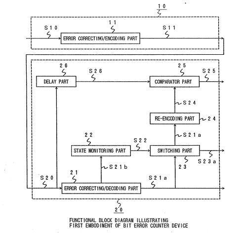
FIG.1 is a functional block diagram illus-trating the
function of a bit error counter device of the first
embodiment o~ the present invention. The bit error
counter device is to be provided on a transmitter
apparatus 10 and a receiver apparatus 20 of ~-
transmitter/receiver equipment for use in dlgital
- 18 ~5~4~
communication, the transmitter apparatus 10 and the
receiver apparatus 20 being .interconnected with each other
through a wire or radio means.
The transmitter apparatus 10 comprises an error
correcting/encoding part 11 for rece.iving an original
signal S10 and outpu~ting a ~ransmission signal S11
The receiver apparatus 20 comprises:
an error correcting/decoding part 21 for receiving a
reception signal S20 and outputting a decoded signal S21a
0 and an overflow signal S21b;
a state monitoring part 22 for receiving ~he overflow
signal S2lb and outputting a switching instruction signal
S22;
a switching part 23 for receiving the switching
instruction signal S22 and the decoded signal S21a and
outputting the decoded signal S21a and the bit error rate
S23a;
a re-encoding part 24 for receiving the decoded
signal S21a outputted from the switching part 23 and
0 outputting a re-encoded signal 524;
a delay part 26 for receiving the reception signal
S20 and outputting a delayed reception signal S26; and
a comparator 25 ~or receiving the delayed reception
æîgnal S26 and the re-encoded signal S24 and outputting
the bit error rate S25.
-~ 19
In what follows, there i~ exemplarily described the
de~ailed construction or the operation of the respective
parts, referring to the a~tached flowcharts.
The transmitter apparatus 10 is first described.
The error correcting part 11 comprises an
initializing part for executing initialization of a
computation region ~or executing convolution-encoding of
the input original signal S10, and a convolution-encoding
part for convolution-encoding the input original signal
S10 and outputting the transmission signal S11.
Successively, the operation of the error
correcting/encoding part 11 is exemplarily described by
reference to the flowchart of FIG.2.
A data forma~ of the input signal is assumed to b~
aO~1), aO(2), ..., aO(n), and a data format of the output
signal to be al(1), a2(1), al(2), a2t2), ..., al(n),
~2(~l)-
In the first place, aO~-4), ~0(-3) t aO(-2), aO(~
aO(O) are initialized (s~ep 201)~ 0 ~zero) is entered
u~ually for initialization. Step 203 is repeated in the
range of lsicn. i is assumed to have been rendered to
initial setting. In~step 203, aO~i) is inputted ~o
calculate
al(i)=aO(i)~aO(i~ aO(i-3)~aO(i-5~,
a2(i~=aO(i)~aO(i-2)~aO(i-3)0aO(i-4)~aO(i-5),
and outputs al(i), a2(i). Thereafter, i is incremented by
+1 and the operation advances ~o step 202. In step 202,
if icn is judged, then the like processing is repeated,
while i>n is judged to be satisfied, then the processing
is completed. ~ denotes an exclusive OR operation.
In the receiver apparatus 20, the error
correc~ing/decoding part 21 comprises an initializing part
for initializing data required for Viterbi-decoding, an
input part for receiving the reception signal S20, a step
1 for branch me~ric operation, ACS operation, path
information determination, overflow control of a path
memory, a step 2 for executing path convergence when the
path memory is judged not to overflow, a step 3 for
outputting th~ overflow signal S21a when the path ~emory
is judged to overflow, a maximum likelihood metric
estimating part for estimating a maximum likelihood
metric, a step 4 ~or determining a decoded value, and an
output part for outputting the decoded signal S21a.
5uccessively, there i9 exemplarily described the operation
o~ the error correcting/decoding part 21 wi~h reference to
the flowcharts of FIGs.3a, 3b~ 3c, 3d, 3e, and 3f. A
trellis diagram and Viterbi-decoding cited in the present
description are e~emplarily illustrated in FIG.3g.
In ~tep 301, there are set i=l, t=2, s2(im)=0~ j=0,
PM(im,1)=im (osims2n~ is assumed.) for initialization.
v~
21
Then, al'(i), a2'(i) are inputted (step 302), and ms2
is judged to be satisfied (step 303). If ms2n~ 1 is
judged to be satisfied, then sl(m)=s2(m) is set (step 304)
while if m<2~1 1-1 is judged to be satisfied, then the
processing is comple-tedO O~ims2nn1-1-1 is assumed as
described above, and im has previously been initialized to
O and is incremented by +1 when step 303 is compleked.
Successively, there will be described the operation of the
step 1 which executes branch me~ric operation, ACS
operation, path information determination with reference
to the flowcharts of FIGs~3b and 3c. Step 305 is to
execute the branch metric operation, i.e., execute
equations given below
x=al'(i)~bl(m,kO)+a2~(i)0b2(m,kO)
y=al'(i)0bl(m,kl~a2'(i~b2(m,kl~
- which is to calculate a Hamming distance (branch metric)
between input signals al'(i), a2'(i), and branch metrics
bl(m,kO), b2(m,kO), bl(m~kl), b2(m~kl~. In this case, the
calculation may be of the sum of products type. Steps 306
20 to 308, and ~tep 312 are those of execu~ing ACS (Add
Compare Select) operation~ First at step 306, a present
branch metric (x,y) is added to a previous branch metric
(sl(kO),sl(kl)). The processing just~mentioned is
e~ecuked by equakions given below.
sx-sl(kO)~x
22
sy=sl~kl)~y -
Successively, sx and sy calculated in step 306 are
compared (step 307), and if 5~Sy iS judged to be
satisfied, then s2(m)=sX is set in step 308, while if 5x~Sy
is ~udged, then s(m)=sy is set in step 312. S~eps 309 to
311, and steps 313 to 315 are those of achieving ~he path
in~ormation determination. First, after step 308 is
completed, a survivor kO (there remains only one path
reaching the respective states~ is inserted into a path ;
memory PM(m,t)(step 309), and PM(kO,im) is inserted into a
work memory WM(m,im) in the range of l~imct-l (steps 310
and 311). In contrast, after step 312 is cornpleted, a
survivor kl is inserted into the path memory PM(mlt)~step
313), and PM(kl,i.m) is inserted i.nto the work memory
WM(m,im) in the range of lsin~t-l (steps 314 and 315).
Herein, im has previously been ini~ialized ~o 1, and after
steps 310 and 314 are done it is incremented by ~1.
Successively, in the ranges of Osins2nl-1 (step 316) and of
lsitst-l, PM~im~it)=WM(im,it) is executed (step 318).
EIerein, im and it have previously been initialized to 1,
and after step 316 or 317 is done, they are incremented by
~1. It should be noted that, though in the step 1 the
processing was done with use of the exclusive OR
operation, the same effect could be expected with use of
the operation o~ the sum of products. In that case, in
23 ~ .3 ~ ~ 5
step 305, there are calcula-ted
x=al (i)xbl(m,kO)-~a2 (i)xb2(m,kO)
y=al'(i)xbl~m,kl)+a2'(i)xb2(m,kl).
Further, in step 307, sX~sy is judged to be satisfied,
and if it i5 SO, when the processing advances to step 308,
while if s~<sy is judged, then the processing advances to
step 312~ and thereafter the same processing is repeated.
Successively, in step 319 (shown in FIG.3a3, t=t-~l is
executed, and t~ml is judged to be sa~isfied (step 320~.
I~ t<ml is judged, then the step 2 is executed, while t~ml
is judged, then the step 3 is executed. ~erein, ml
denotes a path memory length.
Successivelyt there will be described the operation
o~ the step 2 in which oath convergence is executed after
the path memory is judged not to overflow with reference
to the flowchart of FIG.3d. This is the case where the
path memory is judged not to overflow in ~tep 320. More
specifically, in the ran~e of lsms2n~ l, an equation
PM(m,13=PM(O,l)
is judged (step 321), and if all of the a~orementioned
equations are satisfied, step 323 to 330 are executed,
while if even any one of the aforementioned equations is
not satisfied, the processing is terminated. Steps 323 to
330 are described below. Step 323 is a step for
determinin~ a decoded value, in which PM(0,1)~2n~-2 is
24 211 r~
judged to be satisfied (step 323), and if PM(0,1~2nl-2 is
judged to be satisfied, then 1 is inserted into aO'(j~
(step 324), while PM(0,1)<2nl-2 is judged to be satisfied,
then O is inserted into aO'(j) (step 325) to determine a
decoded value aO'(j). i is incremented by +1 (step 326)~
Successively, there will be described steps 327 to 329
where processing is made of shifting the path memory. An
equation PM(m,it)=PM(m,it+1~ is executed (step 329) within
the range of Osms2n~ l (step 327) and within the range of
lsitst-1 tstep 328)~ And t=t-1 is executed ~step 330),
and the proce~sing returns to step 321 for the identical
processing to ~hose described above.
In the ~ollowing, there is described the operation of
a step 4 with reference to the flowchart of FIG.3e, .in
which step 4 the overflow signal S21a is outputted after
the path memory is judged to overflow. In step 320 the
path memory is judged to overflow, and the overflow signal
S21a is outputted (step 331). Steps 332 to 335 are to
evaluate a maximum likelihood metric. There is first
executed initialiæation Mm1=, Smin=sl(O) to evaluate the
maximum likelihood metric (step 332). Then, sl(m)cS~in is
judged (step 334) to be satisfied within the range of
lsms2n~ l (step 333), and if .it is judged to be so, then
Mm1=m, Smin=sl(m) is executed (ætep 335)t while it not so,
then the processing returns to st.ep 3330 Further, when
25 ~i:154~ ~
m>2n~ 1 is judged to hold in step 333, th~n the
processing advances to step 336. Steps 336 to 333 are
those of determining a decoded value. In step 336,
PM(Mm1,1)22n1-2 is judged to be satisfied, and if it is
judged to be so, then 1 is inserted into ao~(i) (step
337), while if PM(Mm1,l)c2nl-2 is judged to be satisfied,
then O is inserted into aO'(j)(step 338). Further, in
step 339 j=j+1 is set. Successively, there will be
described steps 340 to 342 to execute the processing of
shifting the path memory. Thi~ is to execute the
identical processing to that of step~ 327 to 329. More
specifically~ an equation PM(m,i~)=PM(m,it+l) is executed
(step 342) in the range of Osms2n~ 1 (step 340) and in
the range of 15itst-1 (step 341)~ Further, t=t-1 is set
15 ( Btep 343~, and the pxocessing is terminated.
Successively, in step 344 (illustrated in FIG.3a)
1 is set, and i>n is judged to be æatis~ied (step
34S). If icn is judged to be satisfied, then the
processing of from step 302 are repeated, while if i>n i5
judged, then the processing advances to step 346 to
evaluate a maximum likelihood metric. The evaluation of
the maximum likelihood mqt~ic is done in the same manner
as the processing of ~rom step 332 to step 335
(illustrated in FIG.3e).
Successively, there will exemplarily be described the
26 2,1~
operation of the procedure 4 to determine the decoded
value with reference to ~he flowchart of FIG.3f. Within
the range of jcn (step 347), PMIMml,it)~2nl 2 is ~udged to
be satisfied (step 348)o In this case, it varies in the
range of lcitcn-(j-l~ with respect to j at the tLme of
starting of the procedure 4. If PM(Mm1,it)~2n1-2 is judged
to be ~atisfied, then 1 is inserted into aO'(j~ (step
349), while if PM(Mm1,it)<2n1-2 is judged to be satisfied,
then O is inserted into aO~tj) (step 350). Further,
j=j+l, it-it+1 are ~et (step 351), and the processing
returns to step 347. If j>n is thereupon judged, then the
proce3sing is terminated. Further, in s~ep 3~2
(illustrated in FIG.3a), aO'(l), Ø, aO'(n3 are outputted
and the processing is terminated.
The state monitoring part 22 comprises an overflow
signal identifying part for judging whether or not the ~.
overflow signal S21b is inputted, and a switching
instruction signal output part for monitoring the overflow
signal S21b and outputting a switching instruction signal
S22. In the following, there will exemplarily described
the operation of the state monitorin~ part 22 with
reference to the flowchart of FIG.4.
In the first place, 1 is substituted for i for
initialization (step 401). Then, it is judged whether or
not the overflow signal S21b i5 inputted from the error
27 2 ~
corxecting/decoding part 21 (step 402~, and if the
overflow signal S21b is judged to be inputted, then a
counter NOVF for the overflow signal S21b is incremented
by +1 (~tep 403), and in step 404 the same processing is
repeated until i>n is judged to be satisfied. If i>n is
~udqed in step A04, then a set value which has been pxeset
is compared with the counter NOVF (step 405). If the
contents in the counter NOVF are judged to be greater than
the set value, then 1 is inserted into the switching
instruction signal EDF and a switching instruc~ion si~nal
~DF is outputted (step 406), and otherwise O is inserted
into the switching instruction signal EDF which is in turn
outputted (step 407) to terminate the processing.
The switching part 23 comprises a data input part for
receiving the de~oded signal S2la and the switching
instruction signal S11, a decoded signal output part for
outputing the decoded signal S21a, and a set value output
part for outputing the set number of errors and th~ SQt
error rate. Successively, there will exemplarily be
de~cribed th~ op~ration of the switching part 23
constructed as above with referenc~ to the flowchart of
FIG.5. First, the decoded signal S21a is inputted in the
format of aO'(l), ..., aO'(n3, and the switching
instruction ~ignal S22 EDF is inputted (step 501) 9 and the
foregoing switching instruction signal S22EDF satisfies
f~ g ~ a ~
28 ~ ~3 r ~ ~ ~
EDF=l (step 502). Wi~h EDF--0, the input decoded signal
S21a is outputted intactly (step 503), while with EDF=l ,
~here are outputted the number of errors and ~he hit error
rate, which have been preset to between 0 and 50%,
respectively ~step 504).
The re-encoding part 24 possesses the identical
construction to that of the error correcting/encoding part
11, and i~ assumed to be means for re-encoding an input
signal with the aid of the same encoding means as ~he
error correcting/encoding part 11.
The delay part 26 comprises a delay counter initial
value input part ~or inputting an initial value of the -;
delay counter; a counter part for ex0cuting delay
operation with the aid a counter; and a signal output part
for outputting the reception siynal S20. There will.
exemplarily described the operation of the delay part 26
with reference to the block diagram illustrating the
detailed ~unction of FIG~6a and to the flowchart of
FIG.6b.
In the ~irst place, the reception signal S20 is
inputted (step 601). Then, there is outputted a counter
value which has been preset and corresponds to the time to
be delayed this t.ime (step 602), and the counter val.ue is
started (603). The coun~er value i5 a value to delay the
reception si~nal S20 inputted into the delay part 26 by
29
the time during which the reception signal s20 is
processed through the error correcting~decoding part 20,
the state monitoring part 22, the switching part 23, the
re-encoding part 24, and the comparator part 25. Then, a
clock signal is inputted (step 604), and the counter value
is decremented only by one each time the clock signal is
inputted (step 605~. This repeated until the counter
value gets 0 (zero) for execution of step 604 and 605
(st~p 606). In step 606, if the counter value is judged
to be 0 (zero~, then the counter part issues a control
signal (~tep 607) to output the reception signal S20 tstep
608), and the processing i9 terminated.
~ he comparator part 25 comprises a bit comparator
part for comparing the delayed reception signal S26 and
the re-encoded signal S24 with each other for every bit,
and bit error rate evaluation part for evaluating the
error rate S25. Successively, there will exemplarily be
described the operation of the comparator part 25 with
reference to the flowchart~ of FIG.7a and 7b. A data
format when the delayed reception signal S26 is inputted
is assumed to be
al'(l), a2'(1), ..., al'(n), a2'(n),
and a data format when the re-encoded siynal S24 is
inputted is assumed to be
al"~l3, a2"(1~, ... , al~(n)~ a2~n).
2 ~ 4 4 .~
First, l is inserted into i (step 701). Then, al~i) and
al"(i) are inputted (step 702~, and al~(i)=al~[i) is
judged to be satisfied (step 703). If al'(i.3.al"(i) is
judged to be satisfied, then NERR=NERR+l is executed (step
704) and step 705 is executed, while if al'(i)-al"(i) is
judged to be satisfied, then no processing i5 executed and
step 705 i5 executed.
Successively, a2'(i) and a2"(i) are inputted (step
705), and a2'(i)=a2"(i) is judged to be satisfied (step
706). If a2'(i)~a2"(i) is judged to be satisfied, then ~:
NERR=NERR~l is executed (step 707) to execute step 708,
while if al'(i)=al"(i) is judged to be satisfied, then no
processing .is executed and step 708 is executed. Further,
i=i+l is executed (step 708), and nsi is judged to be
satisfied in step 709. Herein, if isn is judged to be
sati~ied, then the processing from step 702 to step 708
is repeated, while if i>n is ~udged, then the bit error
rate RERR is evaluated by dividing the number o~ errors
NERR by a number yielded doubling n in step 710. Further,
the number of errors NERR and the bit error rate RERR are
outputted(step 711), and 0 (zero) is inserted into the
number of errors NERR (step 712~.
Successively, there will be described a second
embodiment o f the bit error counter device.
Referring to FIG.8, there is schematically
31
illustrated the function of a bit error counter device of
the second embodiment of the present invention in the form
of a block diagram. The bit error counter device i.s -to be
provided on the transmitter apparatus 10 and on the
receiver apparatus 20 in the transmitter/receiver
equipment used in digital communication as described in
the first embodiment.
The transmitter apparatus 10 comprises:
an error detecting code evaluating part 27 for
receiving an original signal S10 and outputing an
evaluation result S27 of an error de-tecting code, and
an error correctinq/encoding part 11 for receiving
the ~oregoing evaluation result S27 of the error detecting
code and outputing a transmission signal S11.
The receiver apparatus 20 compri~es:
an error correcting/decoding part 21 for receiving a
reception signal S20 and outputing a decoded signal S21a,
an error d~tector par~ 28 for receiving the decoded
signal S21a and outputing a decoded signal S28a and an
0 error detecting signal S28b,
a switching part 23 ~or receiving the decoded signal
S28a and the error detec~ing signal S28b, and outputing
the decoded signal S28a and the bit error rate S23a,
a re-encoding part 24 for receiving the decoded
signal 528a and outputing a re-encoded signal S24,
32 2 1 1 j 4 ~ 5
a delay part 26 for receiving the reception signal
S20 and outputing a delay~d reception signal S26, and
a comparator part 25 for receiving the delayed
reception signal S26 and the re-encoded signal S24, and
outputing the bit error rate S25.
In the following, there wil].. be exemplarily described
the construction and operation of device detailed portions
with re~erence to the flowchar~s.
There will first be described the transmitter
apparatus 10.
The error detection code evaluating part 27 of the
transmitter apparatus 10 comprises a bit selection part
for selecting most signi~icant m bits from the input
~ignal, and an encoding part for calculating an equation
V(x)-xk/Gcrc(~)-Q(~)~(x)/Gcrc(x)~
and evaluating a remainder polynomial B(x~. Successively,
there will e~emplarily be described the operation of the
error detecting code evaluating part 27 with reference to
the flowchart of FIG.9.
The ~ormat of the input signal is herein assumed to
be
aO(1), aO(2), ... , aO(n-k~, ..
and the format of the output signal is assumed to be
aO(l), aOt2), ..., aO(n-k), ..., aO(n).
It should be noticed that the present embodiment is
4 5
desired to correspond the standard specification of IS54
of US.TIA, so that m=12, k=7, and n=89 axe herein
employed. In ~he first place, the original signal S10 is
inputted in the fon~t of aOIl), aO(2), ..., aO(n-k) ~step
901). Most ~iigni~icant m bits are selected from the input
siignal, and inserted into the data format of
V(l), V(2), ..., V(~l) (n-k)~m
(step 902). Then, V(1), V~2), ..., V(m) yielded in step
902 are used to calculate
V ( x ) Xk/Gcrc ( x ) =Q ( x ) +B ( x ) /G~rC (x) for evaluation of the
remainder polynomial B~x). It is herein assumed that
Gcr~(x) is a generating polynomial, and Q~x) is a division
polynomial, and that the following equation~
V(x)-V(l) x1l+V(2) x1~ +V(12) x
Gcrc(x)=x7+x5+~4+x2+x+1
B(~=V(m+l) x6+V(m+2) x5+- +V(m~k)-x0
are used in the case whare those equations are desirous to
be fitted to the standard specification of IS54 of US.TIA
20 (i~tep 903).
Coefficients of B(x) so ob~ai.ned
V(m~1), V(m~2), .~., V(m~k)
are inserted into
aO(n~k), aO(n-k-1), ..., aO(n) (step 903).
~ resul~ S27 of evaluation of the error detecting code is
34
outputted in a format
aO(1), aO(2), ..., aO(n-k), Ø, aO(n) (step 9043.
The error correcting/encoding part 11 executes the
processing described in the first e~bodiment of the bit
error counter device o~ the present invention, and
receives the result 27 of evaluation of the error
detecting code and outputs the transmitting signal Sll.
Successively, there will be de~cribed the receiver
apparatus 20.
The format on the operation of the error
correcting/decoding part 21 is yielded by eliminating step
316 to 318 in the flowchart in FIG.3c in the first
embodiment o~ the bit error counter device according to
the presenk invention, and eliminating steps 319 and 320,
and the steps 2 and 3 in the flowchart in FIG.3a. The
operation i~ identical to that illustrated in the
flo~Jchart of the first embodiment of the bit error ~ounter
device of the pre~ent invention.
There will be described the error detec~or part 280
The error detector part 28 of the rec~iver apparatus
20 comprises a bit ~elector part for selecting the most
important m bits from the i~put signal, which part is
analogous ~o the error detecting code evaluating part 27,
and encoder part for calculating an equation
V-(x)-xk/Gcrc(x)=~ l(x)/G~r~(
and evaluates a remainder B'(x), which part is analogous
to the error detecting code evaluating part 27, and an
error detecting signal generator part for comparing
coefficients of calculated B~(x) and part of the input
signal with each other and generating an error detecting
signal EDF. In succession, there will e~emplarily be
described the operation of the error detector part 28 with
reference to the flowcharts of FIGs.10 and 11~
It is assumed that the input signal has a format
given below
aO'(l), aO'(2), ..., aO'(n k), ..., aO'(n),
and further EDF'=l or EDF'=O is given.
A processing method is identical to that in the error
detecting code evaluating part 27, i.e., in which method
the decoded signal S2la is inputted in the format of
aO'(1), ..., aO~(n) (step 111), ~he most Lmportant m bits
: are selected from the input signal and are in~rted into
V~(1), ..., V'(m) (step 112), and the remainder polynomial
B'(x) is evaluated (step 113). Mvre specifically, O is
~irst inserted into ~DF' (step 114), and if isk holds,
then step~ 116 and 117 are repeated (step 115). If isk is
judged to hold in step 115, then an equa~ion
V'(m~ aO'(n~k+i) : ..
is judged (step 116) with respect to the coefficients of
the remainder polynomial B'(x) yielded in step 113
36 2 ~ 1 ~J'~
V'(m+1), ~., V'(m~k)
and aO'(n-k+1), Ø, aO'(n)
of the input decoded signal S21a, and if there is existen
any error, then the error detecting signal ~DF~=1 is set
(step 117). Without any error, the processing returns to
step 115, and the identical processing is repeated. ~he
initial value of i is 1 and is incremented by ~1 each tim~
the processing of step 115 is executed. If no error is
detected after a number of the processings of step 115
have been completed, then the decoded signal S28a and the
error detecting signal are outputted in the following
format:
aO'(l~, ..., aO'(n) and EDF'=O,;
while i~ any error is detected, then the same signals are
outputted in the following format;
aO'(l), ..., aO'(n) and EDF'=1.
The switching part 23, re-encoding part 24, delay
part 26, and comparator part 25 employ identical
proces~ing methods to those used in the first embodiment, ~
20 respectively. -
In what follows, there will be described a first
embodiment of a signal identifier device according to the
present invention.
Re~erring to FIG.12, there is schematically
illustrated in the form of a block diagram the function of
a signal identifier device of the first embodiment of the
present invention. The signal identifier device is set to
be provided in a receiver apparatus of
transmitter/receiver equipment for use in digital
communication, the receiver apparatus beiny interconnected
with a transmitter apparatus of the transmitter/receiver
equipment through wire or radio means~
In the following, only the reception side will be
described without any mention to the transmission side.
The receiver apparatus is divided into a speech
signal processor part, a control signal processor part,
and a signal identifier part as processing ~teps.
The speech signal processor part comprises:
an error correcting/decoding part 29 for receiving a
reception signal S20 and outputing a decoded signal S29;
an error detector part 28 for receiving the decoded
signal S29 and outputing an error detecting signal S28b;
a re-encoding part 24 for receiving the decoded
signal S29 and outputing a re~encoding signal S24;
a delay part 26 for receiving the reception signal
$20, and delaying the reception signal S20 by the ~Lme
during wh~ch the reception signal S20 is received by the
error correcting/decoding part 29 is processed by the
error detector part 28 and the re~encoding part 24 and
outputting a delayed reception signal S26; and
. 38
2 ~
a comparator part 25 for receiving the delayed
reception signal S26 and the re-encoding signal S24 and
outputting the number of errors S25,
the control correcting/decoding part 1201 for
receiving the reception signal S1201 and outpu~ting a
decoded signal S1201;
an error detector part 1202 for receiving the decoded
signal S1201 and outputting an error detecting signal
S1202,
10a re-encoding part 1203 for receiving the decoded
signal S1201 and outputting a re-encoding signal S1203;
a delay part 1204 for rece.iving the reception signal
S20, and delaying the recep~ion ~ignal S20 by the time
during which the reception signal S20 received by the
error correcting/decoding part 1201 is procesged by the
: error detector part 12Q2 and the re-encoding part 1203 and
ou~putting a delayed reception signal S1204, and
a comparator part 1205 for receiving the delayed
reception signal S1204 and the re-encoding signal 51203
20 and outputting the number of errors S1205
The signal identif.ier part comprises~
means for inp~tting ~he error detecting ~ignal S28b~
the decoded signal S29, and the number of errors S25 from
the speech signal processor part and further inputting the
error detecting signal S1202, the decoded signal S12Gl,
39
and the number of errors S1205 from the control sig~al
processor part;
means for judging whether the reception signal s20 is
a speech signal or a control signal; and
means for outputting an identification signal, a
decoded signal, and the number of errors.
Successively, there wi]1 be exemplarily described the
detailed constructions or operations of the respective
devic~s.
In the first place, there will be described the
speech signal processor part.
An error correcting/decoding part 29l an error
detector part 28, a re-encoding part 24, a comparator part
25, and a delay part 26 in the speech signal processor
part are constructed and operated in the same manner as in
the ~econd embodiment of the bit error counter device.
Successively, there will be described the control
signal processor partO
An error correcting/decoding part 1201 in the control
~ignal processor part is operated subs~an~ially in the
same n~anner as in the flowcharts each illustrated in
FIGs.3a, 3b, 3c, 3d, 3e, and 3f described in the first
embodiment of the bit error counter device of the present
invention. The following description is only for
opera~ions different from those illustrated in the just-
E ~
~ .
mentioned flowcharts. A format of an input signal isassumed to be
al'(i), a2-(i), a3-(i), a4-(i),
with lsicn, n-65, and nl=res~riction length~ First in
step 301, there are inserted 1 into i, 2 into t, 0 into
S2(im) within ~he xange Of O~ims2n~ O into j, and Lm
into PM(Lm) with the range of Osims2nl-1. Further, in step
302, al'(i), a2~(i), a3~(i), and a4~i) are inputted, and
in step 305 (illustrated in ~IG.3b), the following
equations are calculated.
x-al'(i)~bl(m,k0)~a2'(i)0b2(m,k0)
~a3'(i)~b3~m,k0)~a4'(i)~b4(m,k0)
y=al~ bl(m,kl)+a2'(i)~b2(m,kl)
+a3~(i)0b3(m,kl)~a4'(i)~b4(m,kl)
Operations other than those described above are identical
to that illustrated in the flowchart of FIG.3b.
The error detector part 1202 comprises a data input
part for inputting data, an encoding part ~or evaluating
an equation
A(x) Xl6/Gcrc~(x)=Q~(x)~B (~)/Gcra (x),
and fur~her evaluating a xemainder polynomial B~ and
an error de~ectinq signal generator part ~or com~aring the
coefficients of the evaluated B"(x) and part of the input
signal, and generating an error detecting s.ignal ~DF.
Successively, there will e~empl~rily be described the
, 41 21~
operation of the error detector part 1202 with reference
to the flowchart of FIG.15.
It is herein assumed that the format of ~he input
signal is
aO'(1), ... , aO~(n-k), 0.O, aO~(n),
and the format of the output signal is
aO'(1), ..., aO'(n-k), ..., aO~(n),
and further EDF=1 or ~DF=O.
In procedure 1501, aO~ ..., aO~n-k) are inputted, and
in step 1502,
an e~uation
A~x) }~l6/GCrc ' (X)=Q" (X)+B" (X) /Gcra (X)
i5 calcula~ed. The generating polynomial GCrc~(x) is
assumed to take the form of X16~x12~x5~1. Then, O i.s
inserted into the error detecting signal EDF ~step 1503),
and aO'~n-k~iw~rk)~aO"(n-k+iwrk) is judged (step 1505)
within the range of lsiwrkSk (step 1503~. aO~ (n-k+1),
..., aO"(n) are coefficients of the remainder polynomial
B"~). If aO' (n-k~iwrk)~aO"(n-k+iwrk~ is judged to hold,
then 1 is inserted into the error detecting signal EDF
(step 1506) and the processing advances to step 1504,
while if aO~(n-k~iwrk)=aO"(n-k-~iwrk) is judged, then the
proce~sing advances directly ~o step 1504. Further, if
iwrk>k i5 judged in step 1504, then the processing is
completed.
42
The re-encoding par~ 1203 is means for re-encoding a
control signal (FACCH signal for example), and comprises
an initializing part for initializing a calculation region
for convolution-encoding of the input decoded part for
convolution-encoding the input decoded signal S1201 and
outputing the re-encoding signal S1203. Successively,
there will exemplarily be described the operation of the
re-encoding part 1203 with reference to the flowchart of
FIG.13.
The data format of the input signal is herein assumed
to be
ao~ aO'(2), ..., aO'~n]~
and the data format of the output signal is assumed to be
all'(1), a2"(1), a3~(1), a4~(1),
.. ~, al~(n), a2"(n), a3"(n), a4"(n)0
In the first place, ~here is inserted aO(1) in~o
aO(n~ aO(2) into aO~n~2), aO(3) into aO(n~3), aO(4)
into aO(n~4j, and aO(5) into aOIn+5~ (step 1301~.
Further, within the range of 6siwkcn+5 (step 1302) step
1303 is repeated, and i.~ iwk~n~5 is judged to hold in s~ep
1302, then the processing is completed. In step 1303,
aO(iwk) is inputted, and the:following equations:
al(iwk)-aO(iwk)~aO(iwk-1)0aO(iwk~3)
~3ao(iwk-4)~ao(iwk-5)
a2(iwk)~ao(.iwk~ao(iwk-l)0ao(iwk-2)
_ 43 2~4~
~aO(iwk-5)
a3(iwk)=aO(iwk)0aO(iwk-l~aO(iwk-2)
~aO(iwk-3)~aO(iwk~5)
a4(iwk~=aO(iwk~aO(iwk-2)~aO(iwk-4)
~aO(iwk-5)
are calculated and al(iwk), a2(iwk), a3(iw~), and a4~iwk)
are outputted. rhereafter, iwk is incremented by ~1, and
the processing advances to step 1302, and if iwk~n+5 is
judged to hold, then the processing is completed.
The delay part 1204 and the comparator part 1205 are
con~tructed identically to the delay part 26 and the
comparator part 25 in the speech signal proces~or part,
and hence are operated similarly thereto excepti~g a fact
that a data length in concern is different from the
lat~er.
Successively, there will be described the signal
identi~ier part 1206
The signal processor part lZ06 comprises a data input
part for receiving error de~ecting signals, the number of
errors, and decoded signals, each of which are outputted
~rom both of the spe~ch signa]. processor part and the
control signal pr~cessor part, an input signal judging
part ~or judging whether a reception signal is a ~;peech
signal or a control signalt and an output par-t for
outputing an identification signal that indicates each of
44
the judgment, a decoded signal, and the number of errors.
There will be described the operation of the signal
identifier part 1206 with reference to the flowchart of
FIG.14.
First, ~here will be described two general processing
steps in the signal identifier part 1206.
In the first processing, if the error detecting
signal 528b is judged to be correct, the number of errors
S25 is judged to be larger than the set value 1, the srror
detecting signal S1202 is j~dged to be correct, the number
of errors S1205 is judged to be larger than the set value
3, and the number of errors S25 is judged to be lager than
the number of erroxs S1205, then there are outputted an
FACC~ signal as an identification signal S1206a, a decoded
signal S1201 as a decoded signal S1206b~ and the number of
errors S1205 as the number of errors S1206c.
In the second processing, if the error detecting
signals S28b is judged to be false, and the nu~ber of
errors S25 is judged to be smaller than the set value 2,
then there are outputted a speech signal as the
identification signal S1206a, a decoded signal S29 as the
decoded signal S1206b, and the number of errors S25 as the
number of error~ S1206c.
Success.ively, there will be described a detailed
~5 processing step of ~he signal identifier part 1206. There
2 ~
are first inputted an error detecting signal S25, a
decoded signal S29, and an error detecting signal S28b
each outputted from the speech signal proces~or part 1206,
and an error detecting signal s1205, a decoded signal
5 S1201, and an error detecting signal S1202 each outputted
from the control signal processor park (step 1401). Then,
the error detecting signal S2Bb is judged whether it is
correct or not (step 1402), and if it is correct, then the
number of errors S25>the set value 1 is judged to hold . .
(step 1403). If it is judged to be correct, then the
error detecting signal S1202 is judged to be correct (s~ep
1404), and if it i5 judged to be correct, then the number
of errors S1205>the set value 3 is judged to hold (step
1405), while if the nu~er of errors S1205>the set value 3
is judged to hold, then the number of errors S25>the
number of errors S1205 is judged to hold (s~ep 1~07), and
i~f the number of errors S25>the number of error~ S1205 is
judqed to hold, then ther0 are assumed the identificativn
signal S1206a to be an FACCH signal, the decoded signal ~.
S1206b to be a decoded signal S1201, and the numb.er of
errors S1206c to be the number of errors S1205 (step
1408).
Further, if in step 1407 the number of errors S25sthe
number of errors S1205 i5 judged to hold, then there are
as~umed the identi~ica~ion signal S1206a ~o be a speech
~ 46 2 ~ 1 3~ 4 ~
signal, the decoded signal s1206b to be a decoded signal
S29, and the number of errors S1206c to be the nu~ber of
errors S25 (step 1410).
Further, if in step 1405 the number of errors
S1205sthe set value 3 is judged to hold, then step 1408 is
executed.
Further, if in step 1404, the error detecting signal
S1202 is judged to be false, then the number of errors
S1205<the set value 4 is judged whether it holds (step
1406), and if the number of errors S1205~the set value 4
is judged to hold, the step 1408 is executed while if the
number of errors S1205~the ~et value 4 is judged, then
step 1407 is executed.
Further, if in step 1403 the number of errors S25sthe
set value 1, then step 1410 is e~ecuted~
Further, if in step 1402 the error detecting signal
S28b is judged to be false, then the number o~ errors
S25Cthe set value 2 is judged (step 1~09), and if the
number of errors S25<the set value 2 is judged to hold,
then step 1410 is e~ecuted while if the number of errors
S25~the set value 2 is judged to hold, then step 1404 i5
executed.
After the processing of step 1408 or 1410 is
completed, there are outputted the identification signal
S1206a, the decoded signal S1206b, and the number of
- . 47 2~
errors S1206c (step 1411), resulting in the completion of
the processing. Each of the set values 1, 2, 3, and 4 is
set wi~h the aid of the maximum number of correctable
errors as a reference in an error correcting code to be
used. The set values 1 and 3 may be infinitive, and the
set values 2 and ~ may be 0.
In the following, there will be described a second
embodiment of the signal identifier device of the present
invention.
Referring to FIG.16, there is illustrated in the form ~ :
of a functional block diayram a second identifier device
of the second embodiment of the signal identifier device
of the present invention. The signal identifier device is
to be provided in a receiver apparatus in
transmitter/receiver equipmen~ for use in digital
communication, and is identical to the first embodiment of
the signal identifier device of the present invention in
view of a fact that a transmitter apparatus and the
receiver apparatus are interconnected with each other
through wire or radio means.
In the following, only a reception side will be
described without any mention of a transmission side.
The receiver apparatus is divided into a speech
~ignal processor part, a control signal processor part,
and a signal identifier part.
~8 21~ 5
The speech signal processor part comprises-
an error correcting/decoding part 21 for receiving a
reception signal S20 and outputing a decoded signal S21a
and an overflow signal 521b,
a state monitoring part 22 for receiving the overflow
signal S2lb and outpukting a switching instruction signal
S22,
a switching part 23 for receiving the switching
instruction signal S22 and the decoded signal S21a, and
outputting the switching instruction signal S22 and the
decoded signal S2la,
a re-encoding part 24 for receiving the decoded
signal S21a outputted from the switching part 23, and
outputting a re-encoding signal S24,
A delay part 26 for receiving ~he reception ~ignal
S20, and delaying the reception signal S20 by the time
during which the reception signal S20 inputted into the
error correcting/decoding part 21 is processed by the
state monitoring part 22, the switching part 24 and
outputting a delayed reception signal S26, and
a comparator part 25 for receiving the delayed
reception signal S26 and the re~encoding signal S24, and
outputting the number of errors S25,
the control signal processor part comprises:
an error correcting/decoding part 1201 for receiving
a recep~ion signal S20, and outpu~ting a decoded signal :
S1201 and an overflow signal S1201a, ~:
a state monitoring part 1207 for receiving the
overflow signal S1201a, and outputting a switching
5 instruction signal S1207, ~:
a switching part 1208 for receiving the switching
ins-truction signal S1207 and the decoded signal S1201, and
outputting the switching instruction signal S1207 and the
decoded signal S1201.
a re-encoding part 1203 for receiving the decoded
signal S1201 outputted from the switching part S20, and
outputting a re-encoding signal S1203,
a delay part for receiving the reception signal S20,
and delaying the reception ~ignal S20 by the time during
which the reception signal inputted in~o the error
correcting/de~odin~ part 1201 is processed by the state
monitoring part 1207, the switching part 1208, and the re-
encoding part 1203, and outputtinq a delayed reception
~ignal S1204, and
a comparator part 1205 for receiving the delayed
reception signal S1204 and the re-encoding signal S1203,
and outputting the number o~ errors S1205,
the signal identifier part comprises~
mean~ for inputting the switching instruction ~ignal
S22~ the decoded signal S21a, and -the nun~er of errors S25
~ 50 ~ 4 ~
from the speech signal processor part and further
inputting the switching instruc~ion signal S1207, the
decoded signal S1201, and the number of errors S1205 from
the control signal processor part,
means for judging whether the reception signal S20 is
a speech signal or a control signal, and
means for outputting an identification signal, a
decoded signal, and the number of errors as a result of
the judgment.
Successively, there will exemplarily be described the
construction or operation of each detailed device portion.
First, there will be described the speech signal
processor part.
The error correcting/decoding part 21, state
monitoring part 22, re-encoding part 24, comparator part
~5, and delay part 26 in the speech signal processor part
are constructed identically to those disclosed in the
second embodiment of the bit error counter device t and
hence identical operations ar~ assumed. There will
exemplarily be described the operation of the switching
part 23 with reference to the flowchart of FIG 17. Th~
switching part 23 executes steps 501 and 503 (illustxated
in FIG~5), and judges whether or not E~F=l holds in ætep
502 (illustrated i~ FIG.5)~ If EDF=0 is judged to hold,
then it outputs EDF-0 (step 1701), wh.ile if EDF=1 is ..
51 2 ~
judged to hold, then it outputs EDF=l (step 1702), and the
processing is completed.
Successively, there will be described the control
signal processor partO
An error correcting/decoding part 1201, a delay part
1204, a comparator part 120~, a re-encod.ing part 1~037 and
a state monitoring part 1207 in the control signal
processor part are constructed identically to ~hose
described in the first embodiment of the signal identifier
device of the present invention, and hence are operated
similarly to the latter excepting a fact that a data
length in concern is different from the latter.
There will be exemplarily described the operation o~
the switching part 1208 with reference to the flowchart of
FIG.17. The switching part 1208 executes steps 501 and
503 (illustrated in FIG.5), and it judges in step 502
EDF=1 or not (illuctrated in FIG.5)~ If EDF=0 is judged to
hold, th~n EDF=0 is outputted (step 1701~, while EDF=1 is
judged to hold, then EDF-1 is outputted (step 1702~, and
the proce~sing is completed.
Successively, there will be described the signal
iden-ti~ier part 1206 is constructed identically to the
signal identifier part disclosed in the first embodiment
of the signal identif.ier device of the present invention,
and each switching instruction signal is inputked instead
2 ~
of each error detecting signal followed by the identical
operation to the latter.
INDUSTRIAL APPLICABII,ITY
The bit error identifying method and device according
to the present invention is suitable as disclosed above
for use in land mobile communication such as cordless
telephones, mobile telephones, portable telephones, pocket
bells, simple land radio telephones, and teleterminal
system, maritime mobile communication such as ship
telephones and maritime satellite communication, or
aircraft mobile communication such as aircraf~ public
stations.
Additionally, the method and device are suitable for
use in radio mobile communication-used in varieties of
public organisations, ~CA land mobile radio communication
~ystem~, service self-management communication such as
taxi radio, and particular small power radio stations.