Note: Descriptions are shown in the official language in which they were submitted.
W~ ``4/00954 2 1 1 5 6 ~ 7 Pcl/US93/0605~!i
DESCRIPTION
"Single Sensor Video Imaging System and Method
Using Sequential Color Object Illumination"
S TECHNICAL FIELD
The present invention relates to a method and apparatus
used for processing color images from a sequentially
illuminated object to form high resolution color video
signals suitable for use in viewing the object on a
television monitor.
BACKGROUND ARq~
It will be appreciated by those skilled in the art that
the use of charge coupled devices (CCD) as sensors in video
imaging systems has become quite popular, as, for example,
where small size and low power consumption is desired. In
the processing of color video images, it is preferred for a
number of reasons that a single CCD sensor be used. To that
end, several methods have been developed in the prior art,
one class of which requires sequential illumination of the
object to be viewed, and subsequent processing of signals
from the sensor which represent the level of reflected light
corresponding to each of three primary colors.
Prior art seguential illumination and processing
methods, however, are deficient in either the level of
resolution obtaina~le, in their need for a higher rate of
sampling of data from the sensor, or in their relative
sensitivity. For example, in U.S Patent No. 4,253,447 is
disclosed a sequential illumination process which requires
reading out of only half the field lines (corresponding to
either the even or the odd fields), resulting in a sO~
reduction in vertical resolution. The '447 patent also
discloses a second method whereby the object is sequentially
illuminated by all three primary colors during each of the
odd and even field periods. Unfortunately, this met~od
requires that the CCD data be read at three times the
standard speed which is not always possible. In addition,
this technique requires six field memories and for a given
W094/~g~ PCT/USg3/0605~ -
21156~7
signal-to-noise ratio, it is less sensitive than the current
invention by a factor of three.
Prior art light sources used in conjunction with a
sequential color video camera include: sequentially lighting
the object field with each primary color by rotating a three-
color segmented filter in the path of a white light source;
sequentially illuminating the object with a plurality of
solid state light emitting chips mounted in a single
transparent package, as disclosed in U.S. Patent No.
4,074,306; or sequentially illuminating the object with three
white strobe lights with a different primary color filter in
each of the strobe light paths, as shown in U.S. Patent No.
4,253,447. All of these methods are troublesome.
In some instances it is difficult or inconvenient to
cable video information to a monitor, yet it is desirable to
transmit color video data to a remote site for display and
analysis. It is also in many cases desirable to minimize the
amount of circuitry at the sensor site for applications such
as minimum invasion (laparoscopic) surgery, drill hole
inspections, and the like.
What is needed, then, is an apparatus for sequentially
illuminating an object and processing color images therefrom,
using a single sensor and a minimum of memory devices, and
a flicker-free method of processing video signals from the
sensor without degradation of spatial resolution or
sensitivity, and without the need for accelerated sampling
rates. Preferably, this apparatus should also be adaptable
to applications which would benefit from remote transmission
of video data.
DISCLOSURE OF THE INVENTIO~
An object of the present invention is to eliminate
flicker in a simplified sequential color video system while
maintaining good spatial and temporal resolution.
A further object is to provide for a simplified
sequential light source which uses standard, single-chip
2 1 1 ~ 6 4 7 PCT/US93~ss
mounted light emitting diodes in three primary colors, red,
green, and blue, the outputs of which are synchronized with
the standard field period of a CCD.
To achieve the objective of elimination of flicker,
according to the invention, video data from a color
sequentially exposed CCD is delayed for up to two field
periods in a non-color specific pipeline memory, while
exposure continues for the remaining primary colors at the
television field rate. Using a switching matrix, each of the
primary color signals is tapped from the memory pipeline and
routed to three outputs, one for each primary color. Thus,
each primary color exposure is displayed for three field
periods before temporal updating.
In one embodiment of the device, at least one each of
lS standard, single chip, red, green, and blue light emitting
diodes are used for the illumination source. The diodes are
also sequentially turned on in synchronization with the field
period.
The present invention also lends itself to an embodiment
which provides for simple wireless transmission to a remote
site, in that the use of single-chip light sources integral
to the video sensor head of the device eliminates the need
for fiber optic or other cables connected to an external
light source.
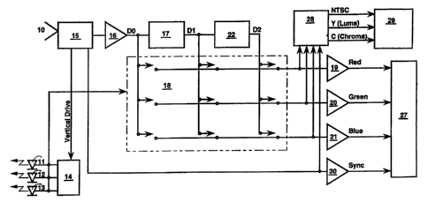
- 2S Figure 1 is a block diagram of a first embodiment of the
sequential color video processing apparatus of the present
invention, in which the light source, sensor, and processing
section are in one unit.
Figure 2 is a bloc~ diagram of the video head-
transmitter unit of a second embodiment of the present
invention, in which~ analog video data is transmitted to a
remotely located receiver-processor unit.
Figure 3 is a block diagram of the receiver-processor
unit of the second embodiment of the present invention.
Figure 4 is a block diagram of t~e video head-
transmitter unit of a third embodiment of the present
~'
W094/0X~ PCT/US93/~r~;
2115647
invention in which data is digitized and transmitted to a
remote receiver-processor unit.
Figure 5 is a block diagram of the receiver-processor
unit of the third embodiment of the present invention.
Figure 6 is a diagram showing the timing relationship
among the respective LED driving signals, standard television
video field periods, and output signals from the A/D and
delay units.
BEST MODE FOR CARRYING OUT THE INVENTION
Referring to Fig. 1, there is shown by block diagram
representation a first embodiment of the apparatus of the
present invention, as well as the basic method by which an
object to be viewed is illuminated and color video image data
is processed. The method begins by illuminating an object
(not shown) with light from a first primary color light
source 11, a red light emitting diode (LED) for example, for
a period of time typically equal to a standard television
field period. Conventionally, this period is 1/60 second.
The red first primary light source 11 is acti~ted for this
field period by one of three outputs from the divide by three
ring counter 1~, which has been selected by the vertical
drive signal of the sensor 15, preferably a conventional
charge coupled device (CCD) assembly, such as the model
CCB/M27 from Sony Corporation of America. However, any
appropriate photo sensor array can be used. The light
reflected from the object is focused onto sensor 15 by a lens
system 10, also of conventional design.
As shown on Figure 6, at the end of the first field
period the vertical drive signal makes a transition and
thereby selects the~ second output of the ring counter 1~,
resulting in the deactivation of the first light source 11
and the activation of the second primary lig~t source 12, a
green LED for example, for one field period. During this
second field period, analog data measuring the response of
sensor lS to first light source 11 is captured by analog-to-
... . ... .
211~6~7
~94/~54 PCT/US93/0605~
.
s
digital (A/D) converter 16 while integration of the second
signal (from second light source 12) is occurring in sensor
15. The output from A/D 16 is provided both to a first
digital delay unit 17 and a matrix switch 18. The first
S delay 17 delays the digitized signal for a time period equal
to one field period.
The output signals of ring counter 1~ are timed and
synchronized such that matrix switch 18 connects the output
of A/D 16 (reference dO on Figure 6) to first digital-to-
analog converter (DAC) 19. First DAC 9 converts the first
captured and digitized primary color signal corresponding to
the first primary color, from first light source 11, back to
analog form, to be used as the odd field video data of the
first primary color signal, red for example.
Following the second field period, the object is
illuminated by a third ?rimary color light source 13, a blue
LED for example, for a third period of time equal to a field
period. This is accomplished by the vertical drive signal i
from the sensor 15 making a transition, thereby deactivating
second light source 12 and activating third light source 13.
During this third field period, the third primary color light
reflected from the object is focused onto sensor 15.
Simultaneously with integration of the third primary color
signal in sensor 15, the analog video signal corresponding
to the level of reflected second primary color light is
captured and digitized by A/D 16. At the beginning of this
third field period, the outputs of the ring counter 14 are
in such a state as to connect the output from the A/D 16 (DO)
to a second DAC 20, and the output from first delay 17 (Dl
on Figure 6) to first DAC 19. Thus, response of the sensor
15 to the first primary color signal, from LED 11, is again
presented at the output of first DAC 9 for the even field
period of the first primary color. The output of second DAC
20 is the analog video signal corresponding to the second
primary color from LED 12, green for example.
Following the third field period, the object is again
:
,
WO 94/009~ 1 7 PCT/US93/~
illuminated with first primary color light source 11 for a
fourth period of time equal to a standard field period. This
is accomplished by the vertical drive signal of sensor 15
making a transition which causes third light source 13 to be
deactivated and first light source 11 to again be activated.
The third color analog signal is captured from sensor 15 and
digitized by the A/D 16 during this fourth field period,
while the first color light signal is again being integrated.
The second color captured and digitized signal is
delayed by first delay 17 and the first color digitized
signal is further delayed by one field period by a second
delay unit 22. At the beginning of the fourth field period,
the outputs of ring counter 14 are such that A/D 16 output
(D0) is connected to a third DAC 21, the output of the first
delay 17 (Dl) is connected to second DAC 20, and the output
of second delay 22 (D2 on Figure 6) is connected to first DAC
19. Also during this fourth field period, the second color
-~ digital signal is reconverted to analog format by second DAC
20 and becomes the odd field of the second color signai, as
shown on Fi~ure 6. Likewise the captured digitized third
primary signal (not delayed) is reconverted to analog format
by third DAC 21 and becomes the odd field of the third color
video signal.
The process continues, in the manner previously
described, according to the timing shown in Figure 6, with
repeated successive second, third, and fourth illumination
periods. It will be apparent to those skilled in the art
that the first field or illumination period is operationally
iden~ical to the seventh field period, except that the first
illumination period begins with sensor 15 and related devices
in a starting or "Q-state" condition. In Figure 6 is shown
the relationship among the drive signals to light sources ~1,
12, and 13, the outputs of A/D 16 (D0), delay 17 (Dl) and
delay 22 (D2), and the even/odd fields of the generated RGB
video field. It should be noted that if precise field period
analog delay lines were available it would not be necessary
~ 94/009~ 2 1 1 5 6 4 7
to digitize the output of sensor 15 and then reconvert it to
analog format. Rather, the sequential analog signals could
be merely switched by matrix switch 18 to their respective
color signal outputs. As an alternative to using an RGB
monitor, the digitized primary color signals and sync signal
can be sent to the inputs of a standard NTSC format
modulator/encoder unit 28, for display on a standard NTSC
format television receiver 29.
The output signals from DAC's 19, 20, and 21, after
processing in the manner described, now correspond to
standard video signals capable of display by a conventional
RGB color television monitor 27, in conjunction with a
standard television synchronization signal obtainable from
sensor 15, through driver-amplifier 30. Accordingly, in the
preferred embodiment, the resulting video image will comprise
conventional odd and even frames or fields of data comprising
typically 262.5 horizontal lines each which are interlaced
and displayed for one standard field period (1/60 second)
each, producing a completed television video image of 525
horizontal lines
Referring to Figures 2 and 3, a second embodiment of the
apparatus of the present invention is shown in which a
separate light source/sensor unit (Figure ~) includes a
transmitter for sending analog color level signals to a
remote receiver-processor unit (Figure 3). In this
embodiment, data from sensor 15 is tagged with a color
identifier signal from ring counter 1~ by means of a
conventional add color ID circuit 23, which tags the video
signal with an identifying pulse denoting which primary color
is then represented by the video signal. The output of the
add ID circuit 23 is then coupled to a wireless transmitter
24 (also of conventional design) from which it is transmitted
to a remote site. Add ID circuit 23 and transmitter 2~ can
be incorporated in the device either prior to or after A/D
16. In the former case the transmission is of analog video
data and in the latter case digital data is transmitted. A
2 1 1 5 6 4 7 PCr/US93/0605 "
conventional color sync signal is also transmitted from sync
driver-amplifier 30.
Referring now to Fig. 3, the transmitted data is then
received by conventional wireless reaeiver 25. A
conventional sync separator circuit 2C strips off the
television synchronization signal, the vertical drive signal,
and the color ID signal. The latter two signals control ring
counter 14 for selecting the appropriate connections to DAC
units 19, 20, and 21. Otherwise the method is identical to
that described with reference to the first embodiment of
Figure 1.
Figures 4 and 5 show yet a third embodiment of the
present invention in which the apparatus of Figures 2 and 3
is modified by relocation of A/D 6 such that transmission
of digital rather than analog data occurs between the
transmitter and receiver units.
Although a variety of conventional electronic components
and sub-systems can be readily adapted for use in the present
invention, in one embodiment A/D 16 is a Brooktree BT208,
delay units 17 and 22 are type NEC 42270, DAC units 19, 20,
and 21 are each a ~rooktree BTl06, counter 1~ is a National
Semiconductor Model CD 4022, and driver-amplifier 30 is an
F.L2020 from Elantec. Matrix switch 18 is a tri-state buffer
type 74HCT244 from Texas Instruments. Of course, it will be
appreciated by those skilled in the art that the resolution
and sensitivity of the apparatus and method of the present
invention are a function in part of the resolution of the A/D
and DAC units, the output levels from light sources 11, 12,
and 13 ! and the sensitivity of sensor 15.
It should be noted that a conventional CCD, as used in
the present inventi~on, is an integrating device, meaning that
its output is not only a function of the intensity of the
light it receives, but such output will continue to increase
for as long as tl~e light source remains on. Consequently,
depending on the sensitivity needed, and the available
intensity of the light sources, it is possible and, in some
21156~7
PCT/USg3/0~5
cases preferable, to activate the primary light sources o~
the present invention for le~s than a complete standard field
period. From a timing point of view in the present
invention, it is only necessary that one primary light source
be activated during each standard field period, for a period
of time equal to or less than such period. Thus, references
herein to an "illumination period" are intended to refer to
the fixed period of time during which a light source will be
activated, and not necessarily the duration of illumination.
Thus, although there have been described particular
embodiments of the present invention of a new and useful
Single Sensor Video Imaging System and Method Using
Sequential Color Object Illumination, it is not intended that
such references be construed as limitations upon the scope
of this invention except as set forth in the following
claims. Further, although there have been described certain
components used in the preferred embodiment, it is not
intended that such references be construed as limitations
upon the scope of this invention except as set forth in the
following claims.
~ ' .