Note: Descriptions are shown in the official language in which they were submitted.
,..".
21 15693 .
TITLE OF THE INVENTION
READER WITH A/D CONVERSION AND
HIGH PRECISE AND HIGH SPEED MODES
BACKGROUND OF THE INVENTION
1. Field of the Invention
The present invention relates to a reader using an image
sensor such as a CCD (charge-coupled device) sensor.
2. Description of the Related Art
Recently, a reader using a CCD sensor has been widely used
as a means for inputting documents and graphic data to a
computer, or an inputting means of each of a digital copying
machine and a facsimile telegraph.
Fig. 9 is a block diagram of a CCD sensor used in such a
reader. In this reader, signals of odd series analog shift
registers and even series analog shift registers are finally
synthesized in a line and outputted. Each of SI, S~, -- , SN
designates a light receiving portion. Each of OSRI, OSR2, -- ,
OSRN/2 designates an odd side shift register for shift-out of
an analog output of each of odd side light receiving portions
arranged in an odd series. Each of ESRI, ESR~, -- , ESR,~~~
designates an even side shift register for shift-out of an
analog output of each of even side light receiving portions
arranged in an even series. BUFF designates a buffer
amplifier. SH designates a start pulse for starting a shifting
operation of each of the shift registers. Each of ~I and ~t~
designates a transfer pulse. ~Q designates a reset pulse.
I
i
-- ~1 15893
CCDOUT designates an output of a charge coupled device (CCD).
Fig. 5 shows a CCD sensor having two output channels.
This CCD sensor can perform a scanning operation at a speed at
least two times in comparison with the charge coupled device
(CCD) shown in Fig. 9. Each of Sl, S2, ---, SN designates a
light receiving portion. Each of OSRl, OSR2, ---, OSRN/2
designates an odd side shift register for shift-out of an
analog output of each of odd side light receiving portions
arranged in an odd series. Each of ESRl, ESR2, ---, ESRN/2
designates an even side shift register for shift-out of an
analog output of each of even side light receiving portions
arranged in an even series. OBUFF designates an odd side
buffer amplifier. EBUFF designates an even side buffer
amplifier. SH designates a start pulse for starting a shifting
operation of each of the shift registers. Each of ~fl and
designates a transfer pulse. Each of SIRE and pIRO designates a
reset pulse. OCCDOUT designates an output of a charge coupled
device (CCD) in each of the odd side light receiving portions.
ECCDOUT designates an output of a charge coupled device (CCD)
in each of the even side light receiving portions.
There is an image reader using such a CCD sensor having
two output channels. In this image reader, each of an odd side
output and an even side output is converted to a digital signal
by an independent AD converter to increase a scanning speed.
Fig. 3 is an explanatory view for explaining the relation
in position between a linear fluorescent lamp 33 and a CCD
2
X1.15693
sensor 37 in a reader. In Fig. 3, an original 31 is arranged
on a glass table 32. The original 31 is separated from the
glass table 32 in this figure. However, in reality, the
original 31 comes in close contact with the glass table 32.
Light is emitted from the fluorescent lamp 33 arranged in a
state in which a longitudinal direction of the fluorescent lamp
33 is perpendicular to a paper face. This light is transmitted
through the glass table 32 and is irradiated onto the original
31. Light reflected on the original 31 is again transmitted
through the glass table and is reflected on a mirror 35. Light
reflected on the mirror 35 is converged by a lens 36 and is
irradiated on a light receiving face of the CCD sensor 37. An
optical unit 34 includes the mirror 35, the lens 36 and the CCD
sensor 37. Reference numerals 38 and 39 respectively designate
a pulse motor and a cabinet.
Fig. 4 is a block diagram of a general reader. In Fig. 4,
reference numeral 40 designates the CCD sensor shown in Fig. 9.
The CCD sensor 40 is connected to an input portion of a buffer
41 through a capacitor C. A power of 5 volts is connected to
this input portion of the buffer 41 through a transistor ASW.
An output portion of the buffer 41 is connected to an input
portion of an AD converter 42. Terminal portions of outputs DO
to D7 of the AD converter 42 are connected to a control circuit
43. A FLON output portion of the control circuit 43 is
connected to an input portion of a lighting device 48. An
output portion of the lighting device 48 is connected to an
3
~1 15693
input portion of a fluorescent lamp 33. If FLON shows value
"1", the fluorescent lamp 33 is turned on.
Terminal portions of outputs TSTEP and FOWARD of the
control circuit 43 are connected to an input portion of a pulse
motor driving circuit 46. An output portion of the pulse motor
driving circuit 46 is connected to an input portion of a pulse
motor 38. When the pulse motor driving circuit 46 receives one
TSTEP pulse at the time of FOWARD = "1", the pulse motor
driving circuit 46 rotates the pulse motor 38 such that the
optical unit 34 and the fluorescent lamp 33 shown in Fig. 3 are
advanced by one step. Similarly, when the pulse motor driving
circuit 46 receives the TSTEP pulse at the time of FOWARD =
"0", the pulse motor driving circuit 46 rotates the pulse motor
38 such that the optical unit 34 and the fluorescent lamp 33
are retreated.
The control circuit 43 has an oscillator 44 and a clock
generating circuit 45 connected to the oscillator 44. The
oscillator 44 oscillates a basic clock signal t0. The clock
generating circuit 45 divides a frequency of the basic clock
signal t0 and generates various kinds of clock signals SH, ill,
~2, ~R and TCLAMP. The clock signals SH, ~1, ~2 and ~R are
transmitted to the CCD sensor 40. The clock signal TCLAMP is
transmitted to a transistor ASW as an analog switch.
Fig. 2 shows timings of clock signals SH, ~1, ~!2 and ~1R as
driving signals transmitted to the CCD sensor 40, a CCD output
signal CCD~UT' a signal TCLAMP for clamping the CCD output
4
~ 1 156 9 3 - _ ___ __ _
signal, and an input signal ADIN transmitted to the AD
converter 42.
Operations of the transistor ASW and the capacitor C shown
in Fig. 4 will next be described with reference to Fig. 10. No
output CCDOUT of the CCD sensor 40 is normally determined with
respect to a direct current (DC) voltage. As shown in Fig. 2,
for example, the output CCDOUT is transmitted in a minus
voltage direction with 4 volts as a reference. This output
CCDOUT is dispersed from 4 V to a voltage value such as 3.5 V
or 4.5 V in accordance with CCD sensors. However, the AD
converter converts an analog potential equal to or lower than 5
V to a digital potential. Therefore, it is necessary to shift
a DC voltage level such that a voltage equal to or lower than 5
V is outputted to the AD converter by the capacitor C and the
transistor ASW. Accordingly, 1 volt is applied to the
capacitor C at any time.
There is a load in a long transmission path of the output
CCDOUT' Accordingly, an amplifier is normally used to amplify
the output CCDOUT' Therefore, noises of this amplifier are
included in this output CCDOUT at random. For example, the DC
voltage level of the output CCDOUT is normally set to 4 V.
However, when this DC voltage of the output CCDOUT is changed
to 3.8 V by the above random noises as shown in Fig. 11, 1.2 V
must be rapidly applied to the above capacitor C. Namely, 1.2
V greater than the normal 1 V by 0.2 V must be rapidly applied
to the capacitor C. Accordingly, when a clamping time t is set
21 15893 .
to 300 nsec and a turning-on resistance R of the analog switch
ASW is set to 50 S~, a capacity of the capacitor C satisfies the
following condition.
CXR « t
C ~ 3 0 0 n s a c / 5 0 S~ = 6 0 0 0 p F
In a general scanner, the capacity of the capacitor C is
selectively set to be equal to or smaller than 1000 pF. As is
well known, an image having reduced random noises can be
obtained in a reader by reliably clamping a DC voltage level of
each of outputs of the CCD sensor. However, as shown in Fig.
2, it is necessary to further set a stabilizing period of the
output CCDDUT before and after the clamp signal TCL~P so that
a basic clock signal is slowly transmitted and a scanning speed
is finally reduced.
As mentioned above, an image having reduced random noises
can be obtained in a reader by reliably clamping the DC voltage
level of each of outputs of the CCD sensor. However, it is
necessary to further set a stabilizing period of the output
CCDCUT before and after the clamp signal TCL~P so that an
operating speed of the reader is reduced.
When two AD converters are used to increase the operating
speed of the reader, AD-converting characteristics are
different from each other in accordance with the AD converters
so that periodic image stripes are caused on odd and even sides
of the AD converters.
6
21 15893 ~~
SUMMARY OF THE INVENTION
It is therefore an object of the present invention to
provide a reader in which a high precise mode or a high speed
mode can be selected in accordance with necessity, and a
reading speed of the reader is increased at a time of the high
speed mode, and a reading operation of the reader can be
performed with high image quality at a time of the high precise
mode.
The above object of the present invention can be achieved
by a reader having a high precise mode and a high speed mode
and comprising animage sensor for separately outputting outputs
of light receiving portions arranged in odd and even series; a
first AD converter corresponding to one of the odd and even
series outputs; a second AD converter corresponding to the
other of the odd and even series outputs; and means for
supplying the other of the odd and even series outputs to the
first AD converter when the high precise mode is selected.
Further, the above reader as a first reader preferably
comprises output selecting means for inputting outputs of the
first and second AD converters thereto. The output selecting
means alternately outputs the outputs from the first and second
AD converters in the high speed mode. The output selecting
means outputs the output from the first AD converter in the
high precise mode.
The above object of the present invention can be also
achieved by a reader having a high precise mode and a high
7
21 15693
speed mode and comprising animage sensor; DC level clamping
means for clamping a DC voltage level of each of image sensor
outputs in the high precise mode and clamping a DC voltage
level of animage sensor output in a unit of one line period in
the high speed mode; and an AD converter for digitally
converting the image sensor output clamped at the DC voltage
level.
In this reader as a second reader, the clamping means
preferably has switching means connected to a clamp voltage
source and a capacitor having a capacity variable in accordance
with the high precise mode and the high speed mode. Further,
the clamping means preferably has clamp pulse generating means
for controlling an operation of the switching means. The clamp
pulse generating means outputs a plurality of clamp pulses
before the image sensor outputs on line in the high speed mode.
No clamp pulse generating means outputs a clamp pulse during
the image sensor outputs on one line in the high speed mode.
Further, the second reader preferably comprises timing
generating means for generating a driving signal of the image
sensor. The frequency of a basic clock signal supplied to this
timing generating means in the high speed mode is preferably
higher than that in the high precise mode.
In the first reader, outputs of the light receiving
portions arranged in odd and even series of the image sensor
are alternately supplied to the first AD converter in the high
precise mode. For example, the output of a light receiving
8
21 1693 v
portion arranged in the odd series is supplied to the first AD
converter in the high speed mode. Further, the output of a
light receiving portion arranged in the even series is supplied
to the second AD converter in the high speed mode.
In the second reader, each of image sensor outputs is
clamped in the high precise mode. The image sensor outputs are
clamped in a unit of one line period in the high speed mode.
Further objects and advantages of the present invention
will be apparent from the following description of the
preferred embodiments of the present invention as illustrated
in the accompanying drawings.
BRIEF DESCRIPTION OF THE DRAWINGS
Fig. 1 is a block diagram of a reader in accordance with
one embodiment of the present invention, in which Fig. 1
comprises Fig. 1 (i) and Fig. 1 (ii) ;
Fig. 2 is a timing chart of signals of a general reader;
Fig. 3 is a schematic view of a reader;
Fig. 4 is a block diagram of the general reader;
Fig. 5 is a block diagram showing the construction of a
charge coupled device (CCD) having two output channels;
Fig. 6a is a timing chart of the reader at the time of a
high precise mode;
Fig. 6b is a timing chart of the reader at the time of a
high speed mode;
Fig. 7a is a basic timing chart of the reader at the time
9
21 15693 -; -
of the high precise mode;
Fig. 7b is a basic timing chart of the reader at the time
of the high speed mode;
Fig. 8a is a diagram of a basic timing generating circuit
at the time of the high precise mode in accordance with one
embodiment of the present invention;
Fig. 8b is a diagram of a basic timing generating circuit
at the time of the high speed mode in accordance with one
embodiment of the present invention;
Fig. 8c is a diagram of an odd side clamp signal
generating circuit at the time of the high precise mode in
accordance with one embodiment of the present invention;
Fig. 8d is a diagram of an even side clamp signal
generating circuit at the time of the high precise mode in
accordance with one embodiment of the present invention;
Fig. 8e is a diagram of the basic timing generating
circuit at a final stage in accordance with one embodiment of
the present invention;
Fig. 9 is a block diagram of a charge coupled device (CCD)
used in the general reader;
Fig. 10 is a view for explaining operations of an analog
switch ASW and a capacitor C; and
Fig. 11 is a view for explaining random noises.
21 15693
DESCRIPTION OF THE PREFERRED EMBODIMENTS
The preferred embodiments of a reader in the present
invention will next be described in detail with reference to
the accompanying drawings.
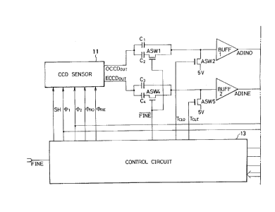
Fig. 1 is a block diagram of a reader in accordance with
one embodiment of the present invention. In this embodiment,
the reader has two operating modes composed of a high precise
mode for reading an image with high precision and a high speed
mode for reading the image at a high speed. The high precise
mode is set when a signal FINE supplied to a control circuit 13
from its exterior shows value "1". The high speed mode is set
when this signal FINE shows value "0". Reference numeral 11
designates a CCD sensor shown in Fig. 5. A terminal portion of
an odd side output OCCDOUT of the CCD sensor 11 is connected to
one ends of capacitors Cl and C2. The other end of the
capacitor C1 is connected to an input portion of a buffer
BUFF1. The other end of the capacitor C2 is connected to the
input portion of the buffer BUFF1 through a transistor ASW1. A
negative output portion of the signal FINE of the control
circuit 13 is connected to a gate of the transistor ASW1. A
drain of a clamp transistor ASW2 is connected to the input
portion of the buffer BUFFl.
An output portion of an odd side clamp signal TCLO °f the
control circuit 13 is connected to a gate of the clamp
transistor ASW2. A source of the clamp transistor ASW2 is
connected to a power source of 5 V. An ADINO output portion of
11
2~1~69~
the buffer BUFF1 is connected to a drain of a transistor ASW3.
A terminal portion of a signal ~2 is connected to a gate of the
transistor ASW3. A source of the transistor ASW3 is connected
to an input portion of a buffer BUFF3. An ADIN1 output portion
of the buffer BUFF3_is connected to a data input portion of an
AD converter AD1. Each of terminal portions of outputs AD~1 to
AD71 of the AD converter AD1 is connected to each of terminal
portions of inputs A~ to A~ of a data selector 12. A T~1
output portion of the control circuit 13 is connected to a T-
input portion of the AD converter AD1.
A terminal portion of an even side output ECCD~UT of the
CCD sensor 11 is connected to one ends of capacitors C3 and C4.
The other end of the capacitor C3 is connected to an input
portion of a buffer BUFF2. The other end of the capacitor C4
is connected to the input portion of the buffer BUFF2 through a
transistor ASW4. A negative output portion of the signal FINE
of the control circuit 13 is connected to a gate of the
transistor ASW4. A drain of a clamp transistor ASW5 is
connected to the input portion of the buffer BUFF2. An output
portion of an even side clamp signal TCLE of the control
circuit 13 is connected to a gate of the clamp transistor ASWS.
A source of the clamp transistor ASW5 is connected to a power
source of 5 V.
An ADINE output portion of the buffer BUFF2 is connected
to a source of a transistor ASW6 and a data input portion of an
AD converter AD2. A drain of the transistor ASW6 is connected
12
~1~15693.
to the input portion of the buffer BUFF3. A terminal portion
of a signal ~1 is connected to a gate of the transistor ASW6.
Each of terminal portions of outputs AD02 to AD72 of the AD
converter AD2 is connected to each of terminal portions of
inputs BO to B7 of the data selector 12. A T~2 output portion
of the control circuit 13 is connected to a T-input portion of
the AD converter AD2. A SELECT signal is supplied from the
control circuit 13 to a SEL input portion of the data selector
12. Each of terminal portions of outputs DO to D7 of the data
selector 12 is connected to an input portion of the control
circuit 13.
Figs. 8a to 8e show a timing generating circuit arranged
within the control circuit 13. Reference numeral 801
designates an oscillator for generating a reference clock
signal. Reference numerals 802 and 807 respectively designate
a counter for 1/12 frequency division and a counter for 1/6
frequency division. Each of reference numerals 803 and 808
designates a decoder. Each of reference numerals 805 and 810
designates a counter for 1/K frequency division. In this case,
K is set to 2048 + 32 = 2080. Each of reference numerals 818
to 822 designates a D-flip flop circuit which can be set and
reset. Terminal portions of outputs QA1, QB1, QC1 and QD1 of
the 1/12 frequency dividing counter 802 are respectively
connected to terminal portions of inputs A1, B1, C1 and D1 of
the decoder 803. The following Table 1 shows the relation
between outputs of the 1/12 frequency dividing counter 802 and
13
2115693 J
the decoder 803.
Table 1
v~ C1.~v~ bt ct dl ct al
I vo o~ a ~ a ht
ai al ~
I ~ tt
a~o o o~ ~
L~ it
~~ct
~
a
a~o~o
o~o~a
L L 0 0 0 0 L 0 0 0 0 0 0 0 0
~ ~ I I I I ~ I
0 0
( f
o L 0 o ( a L o a o o a a a
i , ~ o ~ I i i I ~
o a
~ I
3 L 0 0 0 0 I I , 0 0 0 0 0
( I 0 0 I I ( I
L I I 0
I 0 I
I
l I
II C
IyL 1 0 : ~ 0 0 0 0 0 0
~ ~ 0 ; ( ~ ( ~ ~
0 0 L
i ~
0 0
~ j
The following Table 2 shows the relation between outputs
QA2, QB2, QC2 and QD2 of the 1/6 frequency dividing counter 807
and outputs of the decoder 808.
Table 2
c2.1 d2 e~
9 ~ C ~ ~
f2
0 0. o o.. I.~ o_ o o a
~ ~ ~
o
1 I _0 ~ 0 ~ 0 0 0 0
~ I
2 0 1 0 0 0 1 0 0 0
~ I ~ (
3 I~~ I I 0 0 0 I ~ I 0
( 0 I 0
'
4 0 0~ , 1 0 0. 0 4 ~ 0
0 I
~
~ I 0 I i 0 0 ~ ~ I 1
1 ~ - 0 ~0 0
After the 1/K (in reality 1/2080) frequency dividing
counter 805 is reset, an output OUTl of this counter 805 rises
to a high voltage level by a fall of 2080-th T111. Immediately
14
~1 15693
after this rise, the voltage of an inverted signal T1~1 of
this output OUT1 is reduced to a low voltage level. Thus, each
of the counters 802 and 805 is reset and the flip-flop circuit
819 is set.
After the 1/K frequency dividing counter 810 is reset, an
output OUT2 of this counter 810 also rises to a high voltage
level by a fall of 2080-th T52. Immediately after this rise,
each of the counters 807 and 810 is reset and each of the
flip-flop circuits 821 and 822 is set by an inverted signal
T1~2 of this output OUT2.
After the flip-flop circuit 822 is set by T1~2, this
flip-flop circuit 822 is reset by a rise of output Q2 of the
counter 810. This output Q2 rises from value "0" to value "1"
by a fall of third T52 after the counter 810 is reset.
The decoder 803 generates CCD sensor driving signals y~REl
and ~RO1, an odd side AD converter sampling signal T~O1 and an
even side AD converter sampling signal T~E1 at a time of the
high precise mode. The D-flip flop circuit 818 generates CCD
sensor driving signals X11 and X21 at the time of the high
precise mode. The D-flip flop circuit 819 generates a CCD
sensor driving signal SH1 at the time of the high precise mode.
An OR gate 823 generates an odd side clamp signal TCL01 at the
time of the high precise mode. An OR gate 824 generates an
even side clamp signal TCLE1 at the time of the high precise
mode.
The decoder 808 generates CCD sensor driving signals p~RE2
z~ ~5g93 r
and ~R02, an odd side AD converter sampling signal T~02 and an
even side AD converter sampling signal T~E2 at a time of the
high speed mode. The D-flip flop circuit 820 generates CCD
sensor driving signals p~12 and X122 at the time of the high
speed mode. The D-flip flop circuit 821 generates a CCD sensor
driving signal SH2 at the time of the high speed mode. An OR
gate 825 and an AND gate 827 generate an odd side clamp signal
TCL02 at the time of the high speed mode. An OR gate 826 and
an AND gate 828 generate an even side clamp signal TCLE2 at the
time of the high speed mode.
Reference numeral 831 designates a data selector. A SEL
input portion of this data selector 831 receives a FINE signal.
When FINE = "1" is formed, Yi = Ai is formed. In contrast to
this, when FINE = "0" is formed, Yi - Bi is formed. Terminals
A1, A2 and A3 of the data selector 831 are respectively
connected to terminal portions of signals SH1, X11 and ~t21.
Terminals A4, A5 and A6 of the data selector 831 are
respectively connected to terminal portions of signals ~RO1,
~RE1 and TCLO1. Terminals A7, A8 and A9 of the data selector
831 are respectively connected to a terminal portion of signal
TCLE1° a terminal portion of a logical OR output of signals
T~O1 and T~E1, and a terminal portion of signal T~E1.
Terminal A10 of the data selector 831 is connected to a power
source of 5 V.
Terminals B1, B2 and B3 of the data selector 831 are
respectively connected to terminal portions of signals SH2, t~12
16
21 15693
and X122. Terminals B4, B5 and B6 of the data selector 831 are
respectively connected to terminal portions of signals ~R02,
~RE2 and TCL02' Terminals B7, B8 and B9 of the data selector
831 are respectively connected to terminal portions of signals
TCLE2' TAD02 and T~E2. Terminal B10 of the data selector 831
is connected to a terminal portion of signal ~tl.
Terminals Y1, Y2 and Y3 of the data selector 831
respectively output signals SH, ~J1 and p~2. Terminals Y4, Y5
and Y6 of the data selector respectively output signals SRO,
ARE and TCLO. Terminals Y7, Y8 and Y9 of the data selector 831
respectively output signals TCLE° T~1 and T~2. Terminal Y10
of the data selector 831 outputs signal SELECT.
When the signal FINE shows value "1", the above signals
are respectively set to the following values.
S H=S H1. , ~1 =~1 1 , ~2-=~2 1 , ~RD=~RO1 , $RE=~RE1 ,
T CLO T CLO ' ~ T CLE - T CLE 1 , T AD1 = T ADO ~ '
1 1 0 R . T ADE 1
T 2~ = T 1 SELECT= 5 V
AD ADE
In contrast to this, when the signal FINE shows value °0",
the above signals are respectively set to the following values.
SH=SHZ, '2 2 ~__ 2 __ 2
.~1 ~1 ' ~2 -~2 ' SRO SRO ' ARE ARE '
2 1 __ 2 2 __ 2
T CLO~ T CLO ' T CLE - T CLE ' T AD T ADO ' T AD T ADE '
SELECT= ~ 1
An operation of the reader in the embodiment shown in Fig.
1 will next be explained. In this embodiment, the reader has
17
~1 15893 -
two operating modes composed of a high precise mode for reading
an image with high precision and a high speed mode for reading
the image at a high speed. An operation of the reader in the
high precise mode will first be described. When the high
precise mode is set, signal FINE = "1" is formed. When FINE =
"1" is formed, a negative signal of FINE shows value "0" so
that each of transistors ASW1 and ASW4 is turned off. Only
capacitors C1 and C3 for clamping fulfill their functions at
the time of the high precise mode. For example, capacities of
the capacitors C1 and C3 are equal to each other and are
respectively set to the same constant 1000 pF as a general
scanner. Transistors ASW3 and ASW6 alternately transmit
signals ADINO and ADINE to the ADIN1 input portion of the AD
converter AD1. When FINE = "1" is formed, the SELECT signal of
the data selector shows value "1". Accordingly, at this time,
the data selector outputs an output of the AD converter AD1 at
any time. Namely, DO = ADO1, D1 - AD11, ---, D~ = AD71 are
f o rmed.
In this case, only the output of the AD converter AD1 is
used since no AD converters AD1 and AD2 have the same AD-
converting characteristics and the AD-converting
characteristics are periodically dispersed with respect to odd
and even converters when both the AD converters AD1 and AD2 are
used.
An output OCCDOUT of the CCD sensor 11 is clamped and set
to 5 V by the capacitor C1 and the transistor ASW2. A clamped
18
21 ~15g93
signal is amplified by the buffer BUFF1 and is outputted as
signal ADINO. An output ECCDOUT of the CCD sensor 11 is
clamped and set to 5 V by the capacitor C3 and the transistor
ASW4. A clamped signal is amplified by the buffer BUFF2 and is
outputted as signal ADINE. The signals ADINO and ADINE are
respectively inputted by the transistors ASW3 and ASW6 to the
buffer BUFF3 alternately with respect to time. An output of
the buffer BUFF3 is converted to a digital signal by the AD
converter AD1. Digital signals AD~1, _--, AD~1 are selected by
the data selector 12 and are outputted as D~, ---, D7 to the
control circuit 13.
An operation of the reader in the high speed mode will
next be described. FINE = "0" is formed when the high speed
mode is set. A negative signal of FINE shows value "1". Each
of the transistors ASWl and ASW4 is turned on and capacitors C2
and C4 function as capacitors for clamping. An output OCCDOUT
of the CCD sensor 11 is clamped by the capacitors C1 and C2 and
the transistor ASW2. A clamped signal is amplified by the
buffer BUFF1 and is transmitted to the buffer BUFF3 through the
transistor ASW3. The clamped signal amplified by the buffer
BUFF3 is converted to each of digital signals AD~1, __-, ~,~1
by the AD converter AD1. The digital signals are outputted as
D~, ---, D~ by the data selector and are transmitted to the
control circuit 13. An output ECCDOUT of the CCD sensor ll is
clamped by the capacitors C3 and C4 and the transistor ASW5 and
is amplified by the buffer BUFF2. The amplified signal is
19
~1 15893
converted to each of digital signals AD02, __-, AD~2 by the AD
converter AD2. The digital signals are outputted as D0, ---,
D~ by the data selector and are transmitted to the control
circuit 13.
Figs. 7a and 7b are respectively timing charts of the
reader at the times of the high precise mode and the high speed
mode. Figs. 7a and 7b show timings of a reference clock signal
t0, CCD sensor driving signals ~1 and ~1R0, a CCD sensor odd
side output OCCDOUT and an odd side clamp signal TCLO'
A time of the basic clock signal of the CCD sensor is set
to 12 x t0 in the high precise mode and is set to 6 x t0 in the
high speed mode. The time of the basic clock signal of the CCD
sensor in the high speed mode can be reduced since no clamp
pulse is generated with respect to one output of the CCD sensor
and an output period of the CCD sensor is reduced. A period
about the basic clock signal on one line is calculated as
follows. The number N of pixels of the CCD sensor is set to
2048. 2048 + 32 = 2080 = K basic clock signals of the CCD
sensor are used as one period with respect to a start pulse SH.
In this case, the line period is set to 2080 x 12 x t0 x 1/2 in
the high precise mode and is set to 2080 x 6 x t0 x 1/2 in the
high speed mode. Namely, an operating speed of the reader in
the high speed mode is twice that in the high precise mode. At
the time of the high speed mode, each of the transistors ASWl
and ASW4 is turned on and capacitors for clamping (shifting DC
voltage levels) are constructed by capacitors C1 + C2 and
21 -15~ ~ 9 3 w
capacitors C3 + C4. If t0 is set to 100 nsec, one scanning
period in the high speed mode is set to 0.6 msec. When input
resistances of the buffers BUFF1 and BUFF2 are set to 1 M ~,
capacities of the capacitors C1 + C2 are provided as follows.
(C1+C2) xlMS2»0. 6ms a c
C1+C2~600PF
C1+C2=0. luF
Since C1 « C2 is formed, it is necessary to set C2 to
about 0. 1 ,u F. Simi lady, C4 is selectively set to 0. 1 f.~ F. 1
~ F is about 150 times 600 pF.
Fig. 6a is a timing chart of the reader in the high
precise mode. Fig. 6a shows timings of CCD sensor driving
signals SH, s~l, SRO and ~dRE, a CCD sensor odd side output
OCCDOUT' a CCD sensor even side output ECCDOUT' an odd side
clamp signal TCLO' an even side clamp signal TCLE' an output
ADINO of the buffer BUFF1, an even side AD converter sampling
signal TAO, an output ADINE of the buffer BUFF2, an odd side
AD converter sampling signal TAE, an output ADIN of the buffer
BUFFS, and a sampling signal T~ of the AD converter AD1.
Fig. 6b is a timing chart of the reader in the high speed
mode. Fig. 6b shows timings of CCD sensor driving signals SH,
~1' SRO and ARE, a CCD sensor odd side output OCCDOUT' a CCD
sensor even side output ECCDOUT' an odd side clamp signal TCLO'
an even side clamp signal TCLE' a sampling signal T~1 of the
AD converter AD1, and a sampling signal T~2 of the AD
21
21 15893
converter AD2.
As can be seen from Fig. 6b, only two clamp pulses are
outputted on each of the odd and even sides in the high speed
mode before the CCD outputs on one line. No clamp pulse is
outputted in the high speed mode during the CCD outputs on one
1 ine.
As mentioned above, a reader of the present invention has
a CCD sensor for separately outputting outputs of light
receiving portions arranged in odd and even series; a first AD
converter corresponding to one of the odd and even series
outputs; a second AD converter corresponding to the other of
the odd and even series outputs; and means for supplying the
other of the odd and even series outputs to the first AD
converter when a high precise mode is selected. Accordingly,
no periodic image stripe is caused in the high precise mode by
differences between AD-converting characteristics of the AD
converters so that an image having a high quality can be read.
In the present invention, the reader also has DC level
clamping means for clamping a DC voltage level of each of CCD
outputs in the high precise mode and clamping a DC voltage
level of a CCD output in a unit of one line period in a high
speed mode. Accordingly, the reader can output an image having
reduced random noises in the high precise mode and can output
an image at a very high speed in the high speed mode.
Many widely different embodiments of the present invention
may be constructed without departing from the spirit and scope
22
2115693
of the present invention. It should be understood that the
present invention is not limited to the specific embodiments
described in the specification, except as defined in the
appended claims.
23