Note: Descriptions are shown in the official language in which they were submitted.
211!~73.~
~ 1 -
INTEGRATED CIRCUIT DEVICES WITH
SOLDERABLE LEAD FRAME
Technical Field
This invention concerns integrated circuit devices in which an integrated
5 circuit unit and a lead frame are sealed within a protective enclosure.
Background of the Invention
Integrated circuit (IC) devices, having an integrated circuit (IC) unit and
a lead frame which are sealed within a protective enclosure, find wide use in
products including consumer electronics, household appliances, computers,
10 automobiles, telecommunications, robotics and military equipment. The IC unitencompasses integrated circuit chips and hybrid integrated circuit modules whichinclude one or more of the IC chips and other electronic components on a plastic or
ceramic support base.
A means to electrically interconnect an IC unit to circuitry external of
15 the IC device takes the form of a lead frame. The lead frame is formed from a highly
electrically conductive material, such as copper, copper alloy or an iron-nickel alloy,
by stamping or etching a metal blank into a plurality of leads (or lead fingers)defining a central area in which the IC unit is mounted. The lead frame comprises
typically a mounting paddle and a plurality of separate lead members extending
20 away from a location adjacent to the paddle. In those instances where the paddle is
absent, the leads are formed so that the IC unit is supported by the ends of the leads
or the ends of the leads are positioned in an abutting or spaced position with the IC
unit or the ends of the leads are overlapping the periphery of the IC unit.
The blanked lead frames are, typically, plated in a conventional manner
25 with a layer of nickel over the surface of the lead frame. Nickel plating was intended
to serve as a barrier to diffusion of copper to and formation of reactive copperproducts, such as copper oxides and sulfides, on the surface of the lead frame.
Unfortunately, nickel layer in thickness of less than 400 microinches (10.2
micrometers) contains pores through which migration and diffusion of copper to the
30 surface of the lead frame takes place. However, a layer having thickness of greater
than 400 microinches tends to crack when the leads are eventually bent.
An attempt to elimin~te or at least reduce effects of diffusion of copper
through a less than 400 microinches thick nickel layer was made by depositing a thin
layer of palladium or palladium/nickel alloy on top of the nickel layer. (See
35 European Patent Application No. 0 250 146 published December 23, 1987).
However, copper corrosion products, including oxides, sulfides and other reaction
211~732
products of copper, continued to appear on the lead frame, discoloring the surface of
the lead frame and degrading its solderability. A further attempt to overcome these
shortcomings was made by plating the copper base with a plurality of layers
including, in an ascending order from the copper base, a S microinch (127
S nanometers) thick nickel strike layer, a 3 microinch (76 nanometers) thick
palladium/nickel alloy layer, a nickel layer and a palladium layer. The nickel strike
layer and the palladiurn/ nickel alloy layer were intended to act as a barrier to copper
ion migration to the surface of the lead frame so as to permit the use of a thinner
(less than 400 microinches) nickel layer. (See European Patent Application No. 010 335 608 published October 4, 1989). However, this combination of layers also did
not lead to a product which could withstand the effects of processing steps required
in the process of fabrication of the encapsulated devices. Therefore, there is a need
for a coating or a combination of coatings which could provide satisfactory coverage
of base metals.
15 Summary of the Invention
The present invention embodies a packaged device with a lead frame, a
lead frame and an article of manufacture comprising a base metal, a layer of nickel
on the base metal, and a protective composite of metal layers on the nickel. Thecomposite includes, in succession from the nickel layer, a layer of palladium or soft
20 gold strike, a layer of palladium-nickel alloy, a layer of palladium and a layer of
gold. The palladium or soft gold strike layer acts primarily as a bonding (an
adhesive) layer between the Ni and Pd-Ni alloy layers and as a layer that enhances
reduction in porosity of subsequent layers, Pd-Ni alloy layer acts as a trap for base
metal ions, Pd layer acts as a trap for Ni ions from the Pd-Ni alloy layer, and gold
25 layer synergistically enhances the quality to the Pd layer. The various layers are in
thickness sufficient to effectively accomplished each of their designated roles,depending on the processing and use conditions. Pd or Au strike may be depositedin thickness from I to S microinches, Pd-Ni alloy from 4 to 100 microinches, Pd
from I to 100 microinches and the outer gold layer from I to 100 microinches in
30 thickness.
Brief Descr;ption of the Drawin~s
FIG. I is a schematic representation of a top view of a typical lead frame
with an IC unit mounted thereon;
FIG. 2 is a schematic cross-sectional side view of a portion of an
35 encapsulated device taken along the 2-2 line of FIG. I;
211~732
- 3 -
FIG. 3 is an enlarged schematic representation of a cross-section of a
small longitudinal portion of the lead showing the layers of the composite plating
according to the invention;
FIG. 4 is a plot of an Auger depth profile analysis of a composite
5 according to the invention after being subjected to heat treatment at 250~C for S
hours; and
FIG. 5 is a plot of an Auger depth profile analysis of a composite
without gold flash after being subjected to heat treatment at 250~C for 5 hours.Detailed Description
FIGURE I illustrates a top view of a typical lead frame, 10, for use with
an integrated circuit (IC) unit, I l . The lead frame includes a paddle, 12, on which
the IC unit is bonded, and leads, 13. Dam bars, 14, which interconnect leads 13 at
this stage, are trimmed away after a packaging medium has been applied over an
area shown in phantom lines, 15.
For illustration purposes, this invention will be described with reference
to an IC packaging in which the packaging medium is a molded plastic material,
such as epoxy. However, this invention is applicable to such other embodiments in
which the IC unit and the leads are enclosed in a ceramic or a hybrid ceramic and
metallic package.
In FIG. 2 is shown a schematic cross-sectional side view of a package
16. The package includes IC unit 11, paddle 12; and leads 13. The IC unit which is
bonded on the paddle by solder or adhesive, 17, is electrically connected via wires or
tabs 18, to the leads. IC unit 11, paddle 12, wires 18, and portions of the leads
adjacent to the paddle are enclosed in a molded packaging medium, 19. The leads
25 include a base metal, 20, a layer of nickel, 21, on the base metal, and a protective
composite, 22, on the nickel layer.
The base metal, 20, is typically a copper or a copper alloy. Copper
alloys, such as CDA No. 102 (99.95% Cu, remainder including Ag), CDA No. 103
(99.95% Cu, plus 0.001-0.005 P, and Au), No. 151 (99.9 Cu, 0.1% Zn), No. 155
30 (97.8 Cu, 0.034 Ag, 0.058 P, 0.11 Mg), No. 194 (97.5 Cu, 2.35 Fe, 0.003P, 0.12 Zn),
and KLF 125 (94.55 Cu, 3.2 Ni, 1.25 Sn, 0.7 Si), are representative of the materials
being used for the lead frames. Other alloys, such as iron-nickel alloys may also be
used as the base metal.
The above-identified EP patent applications were primarily concerned
35 with metal coatings suitable for preventing or at least reducing diffusion of copper
and copper products from the base metal to the surface of the leads of the lead frame.
~ S ~9 5 ~ 3 2
However, presence of nickel and nickel products, such as nickel oxide, at the surface
of the leads are of greater concern from the solderability standpoint than the presence
of copper and copper products. Presence of as little as 5 atomic percent or less of
nickel on the surface detrimentally affects the solderability of the surface. Nickel
5 and nickel products, due to the effects of various processing steps, including high
temperature and oxidation conditionsj diffuse to and inter-react with metal
components of the overlaying layers. Nickel products, such as nickel oxides,
interfere with soldering and bonding processes. Besides, they are difficult to remove
with conventional acidic cleaning.
This problem is solved by depositing on top of nickel layer 21 protective
composite 22 having a multilayer structure which in a total thickness of about 10
microinches and more prevents or at least substantially reduces migration of copper
and copper products and of nickel and nickel products onto the outer surface of the
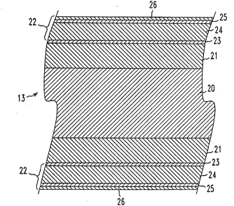
leads. Shown in FIG. 3, is an enlarged schematic representation of a cross-section of
15 a portion of lead 13. Composite 22 includes, in an ascending order from nickel layer
21, a palladium or soft gold strike layer 23, a palladium nickel alloy layer 24, a
palladium layer 25, and a gold layer, 26. The composite is deposited in a total
thickness varying from about 10 microinches to 300 microinches and thicker. The
composite is on a nickel layer ranging typically from 20 to 200 microinches in
20 thickness (510 to 5100 nanometers).
Palladium or soft gold strike layer 23, which acts as a bonding
(adhesive) layer between nickel and palladium-nickel alloy layer is deposited in a
thickness ranging from I to 5 microinches (25 to 102 nanometers). Layers thinnerthan 1 microinch may be insufficient for bonding purposes, while layers 5
25 microinches and thicker would not add any additional advantage. Pd or Au strike
layer is a low porosity layer which, in addition to its bonding characteristics,contributes to an enhancement in growth of subsequent layers with reduced porosity,
which in turn contributes to the reduction in potential diffusion of copper and nickel
toward upper layers. Preferably, Pd strike layer is deposited from a palladium strike
30 solution described in U.S. Patent No. 4,178,475 issued on January 12, 1993 to ~.A.
Abys et al. Examples of compositions and electroplating conditions for depositing
soft gold are disclosed in a book by Frank H. Reed and William Goldie, "Gold
Plating Technology", Electrochemical Publications Limited, 8 Barns Street, Ayr,
Scotland, Third printing 1987, pages 26 and 46.
~ 7 ~ ~
Palladium nickel alloy layer 24 is deposited in a thickness ranging from
4 to 100 microinches (127 to 2540 nanometers). Palladium nickel alloy layer, grown
on the palladium or soft gold strike layer, is a low porosity layer. The main purpose
of this layer is to prevent or at least reduce diffusion of copper, iron and nickel and
5 their products, such as oxides, to the surface of the leads, especially to the surface
which is to be soldered. Layers thinner than 4 microinches may be insufficient to act
as a barrier to diffusion of copper and nickel therethrough, while layers thicker than
100 microinches would not add any additional advantage. The alloy is a Pd-Ni alloy
with nickel content ranging from 10 to 90, preferably from 10 to 30 percent Ni, by
10 weight. The alloy is deposited preferably from a palladium electroplating solution
described in U.S. Patent Nos. 4,911,798 and 4,911,799 both of which were issued on
March 27, 1990 to J.A. Abys et al .
Palladium layer 25, is deposited in a thickness ranging from I to 100
microinches (25 to 2540 nanometers). The main purpose of this layer is to further
1 5 reduce effects of porosity in the under-lying layers and to prevent or at least to slow
down diffusion of nickel from palladium nickel alloy layer 24 to the surface which is
to be used for soldering. Layers thinner than I microinch may be insufficient to act
as a barrier to the diffusion of nickel from the palladium nickel alloy layer, while
layers thicker than 100 microinches would not add any additional advantages. The2 0 thickness of this layer depends on the thickness and the Ni content in the Pd-Ni alloy
layer. The higher the Ni content in the alloy layer, the thicker the Pd layer should be
to prevent or at least to slow down the diffusion of Ni into and through the Pd layer.
The alloy is preferably deposited from palladium electroplating solution described in
U.S. Patent 4,911,799 issued on March 27, 1990 to J.A. Abys et al.
2 5 Gold layer 26 is deposited in a thickness ranging from I to 100
microinches (25 to 2540 nanometers). Layers thinner than I microinch may be
insufficient to provide in combination with the other layers of the composite a
desired diffusion barrier effect while layers thicker than 100 microinches may add
additional expense of the costly gold without adding any additional advantages in
3 0 solderability, solder wettability and bondability of the outer surface. For economical
reasons, the use of the expensive gold layer may for most purposes, be kept at aminimum such as at I or 2 microinches (25 to 51 nanometers). The gold layer may
deposited from any conventional solutions for electroplating gold. Preferably, the
gold layer is deposited as a soft gold strike. Examples of compositions and
211S732
~ - 6 -
electroplating conditions for depositing soft gold are disclosed in a book by Frank H.Reed and William Goldie, "Gold Plating Technology", Electrochemical Publications
Limited. 8 Barns Street, Ayr, Scotland, Third printing 1987, pages 26 and 46.
When the composite is to be used in processing at temperatures of
5 250~C and less, Pd or Au strike layer may be deposited in a thickness of at least one
microinch, the Pd-Ni alloy layer in a thickness of not less than 4 microinches, the Pd
layer in a thickness of at least l and preferably at least 3 microinches, and the outer
gold layer in a thickness of at least l microinch. For processing requiring
temperatures approaching 450~C, the Pd or Au strike may be within the range of
10 from I to 5 microinches, while the minimum thickness of the Pd-Ni alloy layer, Pd
layer and outer gold layer are increased to a range of from 20 to 30 microincheseach.
After completing the metal deposition, the lead frames undergo the IC
unit mounting process. IC units l I are mounted on paddle portions 12 of lead frames
15 l O in a known manner, e.g., by solder or by an adhesive. The electrical connection is
made between the IC units 11 and leads 13 by means of wires or tabs 18. It is
important that the surface of the leads be bondable to the wires. A solderable
surface, which is free of undesirable products of copper and/or nickel, will be also
suitable for bonding of wires thereto. A surface with undesirable products of copper
20 or nickel may not be wire bondable or may be poorly bondable so that a viableconnection may not be established or if established it could become disconnected in
operation. Especially poor contact would be made if the outer surface of the lead at
the place of bond has a thin layer of nickel oxide. Copper products, such as oxides
and sulfides, are removable by cleaning the surface prior to the IC unit mounting,
25 wire bonding and soldering. However, such nickel by-products as nickel oxides are
quite tenacious and are hard to remove with conventional cleaning solutions.
Each assembly is then placed in a molding apparatus, and plastic
encapsulating material is injected around each IC unit and adjacent parts of the leads
and forms an external IC unit package. After removing the assembly from the
30 molding apparatus, the molded IC packages are separated from the lead frames by
separating the ends of the leads from the lead frame and by removing dam portions
between the leads. The leads are then bent into a desirable configuration, e.g., gull
wing, "J" or butt form. Portions of the leads exposed from the molding compound
are cleaned by acid washing and soldered to pads on a mounting board. In one
35 instance the cleaned leads are placed in contact with solder bumps or solder paste on
the mounting board and are soldered to pads on the board by refluxing. In another
211S732
~ - 7 -
instance, the cleaned leads are immersed into a molten bath of solder and then areplaced in contact with fluxed terminal pads on the mounting board.
It is imperative that to have reliable connection between the IC unit and
the mounting board, the leads should have solderable surface. This means that the
5 surface of these portions of the leads which are to be secured to pads on the board
should be capable to receive a substantially continuous coating of solder. A surface
with a solder coating covering 95% or more of the area to be soldered is acceptable
as being solderable. Also, the surface should have a solder coverage with a low
count of pores per square centimeter, such as fewer than 28-30, preferably fewer than
10 25 pores per square centimeter.
In the process of fabricating the encapsulated device, the lead frame
undergoes numerous processing operation steps including those which contribute to
oxidation, interdiffusion contamination, contamination by vapors, cracking, and
contamination surface damaging. The processing steps include injection molding of
15 thermoplastic material to form a plastic frame (150 ~C, 30 minutes), circuit
attachment, heat spreader attachment (150 ~C, 30 minutes), trim and form leads,
oxygen plasma clean or laser H 2 ~ 2 clean to remove any organic impurities, device
attachment including die bond epoxy cure (165 ~C, I hour), cover attach (165 ~C, 1
hour), and burn-in (125 ~C/24 hours) to effect structure stress release and integrity
20 test. These processing steps are well known in the art and do not need any further
detailing. Formation of plastic molded packaging and soldering steps may involvetemperatures as high as 250~C. The processing of ceramic packaging which includes
encapsulation with low-melting glasses may exceed 400~C, falling into a
temperature range of 400 to 800~C for a period of 0.5 hour and longer. These
25 processing steps and resultant unfavorable thermal and oxidation effects on the
material of the lead frame result in reduced solderability quality of the lead frame.
To determine whether or not the surface of the lead frame would be
suitable for a reliable connection, the lead frames with or without the encapsulating
material are subjected to reliability tests. One of the tests is a Military Specification
30 883C, Method 2003 which is used as a qualifying criterion for acceptability. This
standard involves steam aging at 95 ~C and 95% relative humidity for 4, 8 or 16
hours. This is presumed to simulate a shelf life of at least 6 months. Thereafter, the
samples are subjected to an application of non-activated rosin-flux to exposed metal
leads and immersion in solder at 250 ~C for 5 seconds. Samples are then evaluated
35 for solder coverage at 10x magnification. Coatings to be solderability acceptable
must have at least 95% coverage of high-quality smooth solder with a porosity count
211~732
~ - 8 -
of fewer than 28-30, preferably fewer than 25 pores per square centimeter. Although
developed for typical solder finishes, the steam aging test method is applicable in
testing non-solder finished substrates as well. The testing is conducted as if the
surface being tested would receive a coating of solder. The porosity testing is
5 conducted using SO2 vapor as outlined in ASTM B799-88, November 1988, pages
463-465.
Since many applications include thermal exposure of the coated lead
frame, diffusion of metal between the layers under thermal aging conditions may
cause a loss of surface quality if the underlying metal diffuses into the more noble
10 surface layer, e.g., nickel into gold. Therefore, in addition to steam aging, it is
desirable to subject the plated surfaces to a thermal aging. Standardized thermal
aging requirements do not exist at the present time. In order to judge the suitability
of the coatings according to this invention for solderability under different thermal
conditions, the coatings were subjected to thermal testing at 150~C, 200~C and
15 250~C for a period of 1, 2 and 5 hours, and at 450~C for one hour.
The thermal testing was conducted on copper panels having a 20
microinch thick nickel layer coated with a composite having a total thickness of 11
microinches. The composite included, in succession from the nickel layer, a 3
microinch Pd strike layer, a 4 microinch Pd-Ni (80/20) alloy layer, a 3 microinch Pd
20 layer and a I microinch soft gold flash. The sample had greater than 98% solder
coverage, as plated. The sample retained its >98% solder coverage when thermallytreated at 200~C for a period of 1, 2 and 5 hours and at 250~C for a period of 2 and 5
hours. The solder coverage also remained as high (>98%) when the sample was
steam aged (95~C, 95% humidity) for 8 hours.
For comparison, samples were tested having the same Pd strike, Pd-Ni
alloy and Pd thicknesses, but no outer soft gold flash. These samples, rated >98%
solder coverage, as plated, were rated at greater than 98% when exposed at 200~Cfor periods of 1 and 2 hours, and greater than 95% when exposed at 200~C for a
period of 5 hours but fell to an unacceptable value of less than 90% when exposed at
a temperature of 250~C for periods of 2 and 5 hours. Steam aging for 8 hours also
reduced the solderability to a value of less than 90%.
In FlGs. 4 and 5 are shown plots of an Auger depth profile analysis of a
composite having the multilayer composition with in succession from a 20
microinch nickel layer, a 3 microinch Pd strike layer, a 4 microinch Pd/Ni alloy(80/20) layer, a 3 microinch Pd layer and I microinch of soft gold layer. The
composite was subjected to a thermal heat treatment at 250~C for 5 hours. The
- 2 1 1~732
g
sputtering for analysis after the heat treatment was conducted at a rate of 20
nanometers per minute. It is seen from FIG. 4 that no nickel is detected in the Pd
layer for a period of about 3.5 minutes which corresponds to a Pd layer thickness of
about 70 nanometers (approximately 3 microinches). However, FIG. 5 reveals that
5 when a composite with Pd strike layer, Pd-Ni alloy layer and Pd layer of the same
thickness as above, but without an outer soft gold layer, is analyzed, Ni is present at
the surface of the Pd layer. Thus, in 5 hours at 250~C nickel from Pd-Ni alloy will
diffuse into the surface layer of a 2-3 microinches thick palladium layer and interfere
with solderability. However, a I microinch thick layer of gold on top of the
10 palladium layer prevents such diffusion and allows perfect solderability. A similar
situation would arise when the composite with and without the outer gold layer is
subjected to much higher temperatures. For example, in another experiment after I
hour at 450~C, nickel penetrated through 20 micr~inches of Pd and 3 microinches of
gold. This penetration was elimin~ted and complete solderability achieved by
15 introducing 20 microinches of gold on top of 20 microinches of palladium. In
comparison, l O0 microinches of gold alone, that is without the Pd strike, Pd-Ni alloy
and Pd layers, on top of nickel could not prevent the loss of solderability after
thermal exposure at 450~C for only 10 minutes.
In another specific exemplary embodiment individual layers of
20 composite 20 were deposited in succession upon the surface of nickel layer 19. The
composite was deposited in a total thickness of about 12 microinches (about 310
nanometers) upon a nickel layer 20 microinches (510 nanometers) in thickness.
Table I
Combination No.
1 2 3
Layer Thickness in microinches
Pd Strike I 1 2
Pd/Ni alloy 7.5 7.5 75
Pd 1 2
Au Strike 2
The following layered finish, identifiable as combination No. 4
representative of prior art coatings, was used as a control:
211~73~
- 10-
Layer Thickness
in microinches
PdNi Strike 3
Nickel 20
Pd 3
Samples were tested for solderability as-plated and following 8 hours steam aging.
Porosity testing was performed on sections cut from the same panel used for the
solderability testing. The solderability and porosity performance results of themultiple layers are presented in Table II.
Table II
Comb.No. 1 2 3 4
% Coverage
as-plated 99 99 98 97
% Coverage
steamaged 98 97 97 85
Porosity
count
pores/ cm2 11 13 23~100
Additional advantages and modifications will readily occur to those
20 skilled in the art. Therefore, the invention in its broader aspects is not limited to the
specific details, representative devices, and illustrated examples shown and
described. Accordingly, various modifications may be made without departing fromthe spirit or scope of the general inventive concept as defined by the appended claims
and their equivalents.