Note: Descriptions are shown in the official language in which they were submitted.
WO93/~67D0 2116128 PCT/U592/07689
DIMMING CONTROL CIRCUIT
BACKGROUND OF THE INVENTION
1. Field of the Invention
This invention relates generally to dimming
control circuits for lighting fixtures and, more
particularly, to dimming control circuits that include ac
power sources and semiconductor power switches.
2. Description of the Related Art
Dimming control circuits of this particular kind
are commonly used in many applications, including theater,
television, and architectural lighting applications. In
such ap]plications, a number of banks of separate lighting
fixture~s are typically included, with the dimming control
circuit independently controlling the light intensity
provided by each fixture or group of fixtures. Continuous
control is generally pxovided, from full intensity down to
zero intensity.
An example of a conventional dimming control
circuit of this particular kind is depicted in FIG. 1. It
includes an ac power source 11, a dimmer rack 13, and a
plurality of lighting fixtures 15a-15d. The power source
delivers ac electrical current over a pair of lines 17 to
the~dimmer rack, and the dimmer rack controllably directs
~selected~amounts of ac current to the various lighting
fixtures over separate pairs of wires l9a-19d. The
lighting fixtures can be connected to their associated
pair of wires by conventional three-prong plugs and
sockets 21a-21d. The third prongs of the associated plugs
and sockets are connected to ground via wires 22a-22d.
The dimmer rack 13 includes separate switching
circuits 23a-23d for controllably switching the electrical
current being supplied to the lighting fixtures 15a-15d,
. .
W093/0670~ - PC~/US92/07689
21~6128 2 ,~
respectively. Each switching circuit includes, in series,
a circuit breaker 25, an inductor or choke 27, and two
silicon-controlled rectifiers (SCRs) 29a and 29b arranged
in parallel, oppo~ed relationship. The SCRs are
controllably switched ON by an appropriate control signal
supplied on line 31a from a controller 33 that is part of
the dimmer rack. Each SCR is switched ON at a selected
time during each successive cycle of the ac electrical
power, to provide the desired degree of dimming. The
choke is provided in each switching circuit to reduce
audible and electrical noise that otherwise could arise
from a rapid change in electrical current magnitude. As
is conventional, the SCRs can be substituted by a single
triac.
FIG. 2 shows several waveform diagrams useful in
understanding how each switching circuit 23a-23d controls
the intensity of light emitted by its associated lighting
fixture 15a-15d. ~his intensity control is achieved by
controlling the time at which the SCRs 29a and 29b are
switched ON during each cycle of the ac electrical power.
Two full cycles of the ac power signal are depicted in
line (a), and the control signal coupled to the control
electrodes of the parallel, opposed SCRs is depicted in
line (b). This control signal includes a series of pulses
of uniform width, each pulse occurring during a separate
half cycle of the ac power signal. Each pulse functions
to switch ON whichever of the two 5CRs is forwardly biased
at that time. Because the same control signal is applied
to both SCRs, and because the two SCRs are connected in
parallel, opposed relationship, they are switched ON in an
alternating fashion and they cooperate to supply a current
like that depicted in line (c) of FIG. 2. The rms value
of this pulsed ~urrent controls the intensity of light
that the associated lighting fixture will emit.
In another prior dimming control circuit,
.
.. - , . . ... ... .. . .
W093/06700 2 ~ 2 8 PCT/US92/076~9
-3-
described in ~.S. Patent No. 5,004,957, the control signal
includes just a single pulse for each cycle of the ac
power signal. Only one SCR of the pair is used in the 0~
to 50~ brightness range, but both SCRs are used in the so%
to lOO~ brightness range. This provides reduced acoustic
and electrical noise, because of the control signal's ~ -
reduced operating frequency.
The conventional dimming control circuits of the
kind described above function generally satisfactorily in
providing a-continuous control of the intensity of light
emitted by a series of lighting fixtures. Nevertheless,
it is believed that these conventional dimming control -~
circuits are unduly inefficient, requiring significantly
more ele!ctrical components and interconnecting power lines -
than are necessary. It should, therefore, be appreciated
that there is a need for a more simplified dimming control
circuit, which can operate to control the light output of -
a number of lighting fixtures, with a reduced number of
electrical components and interconnecting power lines.
The present invention fulfills this need.
SUMMARY OF THE INVENTION
~ This invention is embodied in a dimming control
circuit for a plurality of lighting fixtures, which
operates efficiently in directing selected a~ounts of -~
electrical current from an ac power source to each
lighting fixture. The circuit includes a plurality of
semiconductor power switches (e.g., silicon-controlled
rectifiers, or SCRs), each connected between the ac power
source and a separate lighting fixture, and each adapted
to couple electrical current to its associated fixture in
only one direction. Phase control signal generator means
are provided for generating a plurality of independent
control signals, each for coupling to the control
electrode of a separate semiconductor power switch, to
2 1 ~ 8
. .. . . ~ ..
It also is known to place diodes in series with a light fixture
in non-dimming circuits, to limit the application of electrical
current to just one half of a standard ac power waveform or to `:
jus~ one dc polarity. An example of such a use of a diode is
disclosed in German Patent No. DE 40 05 012 Al. ::
JGi k
~ JJ~
S~J ~
$~ Y
;
.~SUBSTITUTE SHEET
CU 23021 WO PA K~hler, K~ck & Fiener 27. Oktober 1993
W093/067~ 2 1 1 6 1 2 8 PCT/US92/076X9
,
--4--
condition that switch to couple a selected amount of
electrical current to the associated lighting fixture only
during the positive half cycles, or only during the
negative half cycles, of the ac electrical power. In this
fashion, the number of semiconductor power switchçs is
reduced to just one per lighting fixture. In addition to
including a reduced number of electrical components, the
dimming control circuit of the invention couples power to
the lighting fixtures over fewer interconnecting power
lines.
:
In one embodiment of the invention, the hardware
of a conventional dimmer rack is used in an unmodified
form, but the software used in its controller is modified
to provide separately-controlled pulses for the positive
and negat:ive half cycles of the ac power coupled to an
associated pair of lighting devices. Thus, positive
current pulses of selected duration are interleaved with
negativ-e--~ current pulses, of independently-selected
durationj for coupling over a common pair of power lines
to an associated pair of lighting fixtures. At the
location of those lighting fixtures, two diodes arranged
in reverse directions couple either the positive current
pulses or the negative current pulses to the appropriate
lighting fixture;
In an alternative embodiment, a separate
semiconductor power switch is connected to couple
electrical power directly to each lighting fixture,
without the need for an additional diode. Like the first
embodiment, electrical current is supplied to the lighting
fixture only during either the positive half cycles or the
negative half cycles of the ac power. In this case, the
semiconductor power switches are preferably located
remotely, at the sites of the lighting fixtures being
controlled, and the chokes can be located either
centrally, in the dimmer rack itself, or remotely, at the
` ` 2 1 ~ 8 .
. .
sites of the lighting fixtures..
Other features and advantages of the present
invention should become apparent from the foliowing ~- ;,.
description of the preferred embodiments,' taken in
conjunction with the accompanying drawings, which
illustrate, by way of example, the principles of the
invention.
.
BRIEF DESCRIPT~ON OF THE DRAWINGS
FIGS. 1 and lA are simplified schemati.c bloc~
diagrams of a conventional dimming control circuit, for
providing independent dimming control for four separate
lighting fixtures.
FIG. 2 is a timing diagram showing the ac power
signal and an exemplary control pulse signal and the
resulting switched power signal for one lighting. fixture
in the dimming control circuit of FIG. 1. ~ :
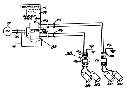
FIGS. 3,. 3A and 3B are .simplified schematic
block diagrams.of a first embodiment of a dimming control , . .'
: circuit.in accordance with the invention, th~s embodiment
.
utilizing the hardware of a conventional dimming 'control
circuit like that of FIG. 1, but requiring only one-half
the number of switching circuits to ::control the same
numbex of lighting fix~ures. ,.,'.
.FIGS. 4 and 4A are simplified sche~atic block
diagrams of a second em~odiment of a d'imm'ing, ~ontrol
circuit in accordance with'the in,~ention, this embodiment
having. its controller an~ semiconductor 'power 'cwitches
located remotely, at"or near the sites of the lighting
fixtures being controlled.
,
FIG. 5 is a timing diagram showing various
`
W093/06700 ~ PCT/~S92/~7689
2 ~ 2 8
-6-
exemplary signal waveforms present in the dimming control
circuits of FIGs. 3 and 4.
DESCRIPTION OF THE_PREF_RRED EMBODIMENTS
... . -~
With reference now to the drawings, and
particularly to FIG. 3, there is shown a dimming control
circuit for supplying controlled amounts of ac electrical
current to a plurality of remote lighting fixtures, four
of which are identified by the reference numerals 35a-35d.
The dimming control circuit includes an ac power source 37
and a dimming rack 39 for independently controlling the
amount of electrical current coupled to each of these
lighting fixtures, thus controlling the intensity of light
emitted by these lighting fixtures. The hardware portion
of the dimmer rack is identical to that of the
conventional dimmer rack depicted in FIG. 1. However, the
software portion of the di~mer rack, which is implemented
by its controller 41, operates such that each of the ;
dimmer rack's switching circuits is conditioned to supply
controlled amounts of electrical current, independently,
to two separate lighting fixtures, rather than merely one.
Two of these switching circuits are identified in FIG. 3 -
by the reference numerals 43a and 43b.
;'~;
Power is delivered to the two switching circuits
43a and 43b from the ac power source 37 via lines 45,
includi~g a supply line and a return Iine, and two sets of
power lines 47a and 47b, each including a supply line and
a return line, supply el~ctrical power from the two ~ -~
switching circuits to their associated pairs of remote
lighting fixtures 35a and b and 35c and d. The two sets
of power lines supply the power to a remote socket 49a or
49b for each pair of lighting fixtures, and a special
adapter 51a or 51b plugs into each socket to separate the
supplied power into two separate power signals, one for
each lighting fixture. ~hus, a substantial reduction in
2~1~128
W093/06700 PCT/US92/076~9
.:
-7-
hardware components and interconnecting wiring is
provided.
More particularly, each switching circuit 43a or
43b in the dimmer rack 39 includes a circuit brea~er 53,
an inductor or choke 55, and first and second silicon-
controlled rectifiers (SCRs) 57 and 59 arranged in
parallel, opposed relationship. The controller 41, which
is part of the dimmer rack, provides a control pulse
signal on line 61a or 61b to the control terminals of the
two SCRs, to controllably switch the SCRs ON at selected
times during each half cycle of the ac power signal.
In the dimming control circuit of FIG. 3, the
controller 41 provides a separate control pulse signal for
each switching circuit 43a or 43b that independently
controls the two SCRs 57 and 59 in each switching circuit.
Thus, the successive pulses of the control pulse signal
that are associated with the positive half cycles of the
ac power signal have durations determined in accordance
with the desired light intensity for the first lighting
fixture 35a, while the pulses associated with the
successive negative half cycles have durations determined
in accordance ~with the desired intensity of the second
liyhting fixture 35b.
An exemplary control pulse signal is depicted in
FIG. 5(b), where it will be noted that the puIses
associated with the positive half cycles are substantially
narrower than the pulses associated with the successive
negative half cycles. Consequently, the switched ac power
signal provided by the switching circuit 43a will be as
shown in FIG. 5(c). This pulsed power signal is
transmitted over lines 47a to the remote socket 49a. As
previously mentioned, an adapter 51a can be plugged into
the socket to separate out the alternating positive and
negative pulses, for coupling to the respective lighting
:
. ~ .
2~1~128
.
., . ;
- . . .
-8- ' ~'
fixtures 35a and 35b. . .:
As shown in FIG. 3B, the adapter 51a ~ :
accomplishes this separation in a straightforward'manner
using first and second diodes 63 and 65. The adapter
itself includes two sockets 67 and 69, to which the
respective lighting ~ixtures 35a and 35b can be releasably
connected. One of the two incoming power lines 47a is
connected through the first diode 63 to on'e terminal of ,
,the first socket 67, while that same incoming,power.line
is connected through the second diode 65 to one terminal
of the second socket 69. The other of the incoming power :~
lines 47a is connected through the adapter directly to .
second t:erminals of the two socXets 67 and 69, while a :;:~
ground line 71a likewise is connected through the adapter
directly to third terminals of the two sockets.
The first diode 63 of the adapter 51a transmits
to the ~irst socket 67 only the positive pulses of the ~ '
alternating positive and negative power pulses of the ,
pulsed power signal on lines 47a (FIG. 5(c)), while the ,':
second diode 65 transmits to the second socket 69 only the
negative power pulses of that pulsed power signal. Thus, .
the first diode transmits to the first socket a power
signal like that depicted in FIG. S(d), while the second
:diode transmits to the secand socket a power signal like
~ that depicted in FIG. 5(e). It will be appreciated that
the rms power supplied to the first lighting fixture 35a
is thus. controlled by the duration of ~he control pulses : ~'
occurring only during the positive half cycles of the ac ,;,,,
power signal supplied by,the powèr source 37, while the
rms power supplied to the second fixture 35b is controlled
by the duration of the pulses occurring during the
negative half cycles. Because these pulse durations are
independently controlled, the light intensities provided ' .
by the two fixtures li~ewise are independently controlled. -~
In addition, because each lighting fixture receives
W093/06700 2 1 1 6 1 2 8 PCT/U~92/07689
electrical current pulses having a frequency equal to the
fundamental frequency of the ac power signal, typically 60
Hz, rather than double that fundamental fre~uency, audible
noise and electrical noise are reduced.
.. . : ,
It also will be appreciated that the dimming
control circuit of FIG. 3 provides a marked reduction in
the number of electrical components over the conventional
dimming control circuit of FIG. 1. In particular, each
switching circuit 43a or 43b is adapted to controllably
power two separate lighting fixtures, as contrasted with
one such switching circuit required in the past to power
each fixture. In addition, just a single pair of power
lines 47a or 47b is required for each pair of lighting
fixtures, as contrasted with a separate pair of power
lines required in the past for each lighting fixture.
Because t:he lighting fixtures frequently can be located at
great distances from the dimmer rack 39, this reduction in
wiring can lead to significant cost savings. In the U.S.,
most building codes require the use of a minimum wire size
having a current-carrying capability, or ampacity,
significantly greater than the needs of each lighting
fixture. Consequently, because the invention enables two
fixtures to be independently serviced by the same pair of
power lines, the lines' excess ampacity can be utilized
and a greater cost efficiency therefore can be achieved.
Further, because the hardware of the dimmer rack 39 is
identical to that of conventional dimming control
circuits, the invention lends itself to a convenient
~ retrofit of circuits already in use.
Still another advantage of the dimming control
circuit of FIG. 3 is that coupling current to the lighting
fixtures only on alternative half cycles of the ac power
reduces the rms voltages applied to the fixtures. This
can lead to a greater operating efficiency, because it is
known that reducing the applied rms voltage, while
W093/06700 PCT/US92/076Xg
211~128 -- -
-10- ~,
correspondingly increasing the electrical current so as to
maintain the same wattage, will provide increased emitted
lumens. Moreover, this reduced rms voltage is achieved
without the need for a step-down transformer.
. . :
With reference now to FIG. 4, there is shown an
alternative embodiment of a dimming control circuit in
accordance with the invention. This embodiment includes
an ac power source 73 and a circuit breaker panel 75 for
supplying electrical power to a plurality of lighting
fixtures, four of which are identified by the reference
numerals 77a-77d. In this embodiment, SCRs for providing
pulsed electrical current are not located in a central
dimmer rack, but rather are located remotely, at the sites
of the lighting fixtures being controlled. This
lS eliminates the need for separate diodes, as in FIG. 3 -
embodiment, to provide positive current pulses ~to one
lighting fixture and negative current pulses to another. ~
' . ':
More particularly, the circuit breaker panel 75 ~;
of the dimming control circuit includes a plurality of
circuit breakers, two of which are identified by the
reference numerals 79a and 79b. These circuit breakers
pro~ide power to separate, remote switching circuit 81a or
81b, which in turn provide controllably switched power to
a plurality, e.g., four, of lighting fixtures. The
25 switching circuits are controlled by a controller 83 that -~
is located remotely, in the general vicinity of the -~ ~-
lighting fixtures 77a-77d. Ac power is delivered from the
ac power source 73 to the circuit breaker panel on lines
85, and the circuit breaXer panel in turn supplies power
to the two switching circuits 81a and 81b on pairs of
lines 87a and 87b, respectively.
:; ~ .
Each of the switching circuits 81a and 81b
includes a single inductor or choke 89 and two SCRs 91 and
211~12~
W093/06700 PCT/US92/07689
,__
93, for controllably supplying pulsed electrical current
to two sockets 95 and 97, to which can be selectively
connected two separate lighting fixtures. In particular,
one line of the pair of power lines 87a or 87b is
connected through the first SCR 91 to one terminal of the
first socket 95, and through the second SCR 93 to one
terminal of the second socket 97. The second line of the
pair of power lines 87a or 87b is connected directly to
separate terminals of the two sockets 95 and 97, and a
ground line 99a likewise is connected directly to separate
terminals of the two sockets 95 and 97. The control
electrodes of the two SCRs 91 and 93 receive a control
pulse signal supplied on line lOla from the controller 83.
It will be appreciated that the dimming control
circuit embodiment of FIG. 4 operates similarly to the
circuit embodiment of FIG. 3,~ except that the diodes 63
and 65 of the FIG. 3 ~bodiment are eliminated because the
output t;erminals of the two SCRs 57 and 59 are no longer
ganged together. Thus, for a control pulse signal of the
form depicted in FIG. 5(b), the first SCR 91 will transmit
to the first socket 95 an electrical current signal like
that depicted in FIG. 5(d), and the second SCR 93 will
transmit to the second socket 97 a current waveform like
that depicted in FIG. S(e).
The FIG. 4 embodiment is configured such that
the controller 83 can be located closer to the sites of
the switching circuits 81a-b and the lighting fixtures
77a-d. This significantly reduces the need for using long
runs of control lines. In addition, the circuit breaker
panel 75 can be a standard, off-the-shelf item. In this
embodiment, the chokes must be selected to emit reduced
audible noise, because they are located at or near the
W093/06700 PCT/US92/07689
211~2~
-~2-
sites of the lighting fixtures, rather than in an isolated
control room.
In another alternative embodiment, similar ~o
FIG. 4 but not shown in the drawings, the chokes ar~ ~oved
from the switching circuits back to the circuit breaker
panel. This configuration is desirable in situations
where low-noise chokes are unavailable and where acoustic
noise at the sites of the lighting fixtures must be
minimized.
lo In a variation of all of the embodiments
described above, each choke and SCR can be substituted by
a series-connected diode and transistor. Suitable
transistors include bipolar transistors, field-effect
transistors (FETs), and insulated-gate bipolar transistors
15 (IGBTs) . By operating the transistors in a linear mode,
the equivalent function of an inductor can be effected.
:'':
It should be appreciated from the foregoing
description that the present invention provides an
improved dimming control circuit that can provide
controlled amounts of pulsed ac power to a plurality of
lighting fixtures, with substantially fewer electrical
components and interconnecting power lines. Several
circuit embodiments are disclosed, all of them including
a single semiconductor power switch, e.g., a silicon-
controlled rectifier, for coupling controlled amounts ofpulsed electrical current in just a single direction,
either positive or negative, to each lighting fixture.
Although the invention has been described in
detail with reference only to the presently preferred
embodiments, those of ordinary skill in the art will
appreciate that various modifications can be made without
departing from the invention. Accordingly, the invention
is defined only by the following claims.