Note: Descriptions are shown in the official language in which they were submitted.
WOg3/04541 PCT/USg2/07030
21~228
MULTIPORT Mn~TIDROP DIGITAL SYSTEM
BACKGROUND OF THE INVENTION
This is a continuation of U.s. Serial No. 07/749,897,
which is hereby incorporated by reference in its entirety
herein.
1. Field of the Invention
This invention relates generally to telecommunications
systems. More particularly, it relates to digital multiport
multidrop systems where a plurality of hosts are coupled via a
single line to a digital telecommunications network and
communicate with data terminals, where a first group of data
terminals are coupled via a first single line to the digital
telecommunications network and a second group of terminals are
coupled via a second single line to the digital
telecommunieations network.
The invention is particularly applicable in the banking
industry where it may be desirable for banks to have
information from tellers, ATMs and security systems on a
single line at various branches communicating with separate
hosts for tellers, ATMs and security systems at a single
different location. -
- ' '
2. State of the Art ~
Different multiport multidrop systems have been proposed.
U.S. Patent number 4,858,230 to Duggan, for example, discloses
an analog system where outbound messages from hosts are
multiplexéd and sent on a constant earrier over a single line
to data terminals. Return messages from~data terminals are
similarly sent. However,~since only onè data terminal can use
the line at any given time, responses from different terminals
need to be delayed.
W093/04~l PCT/US92/07030
21i6228 2
Recently, digital multiport multidrop systems have been
proposed by Racal-Milgo and Paradyne. Digital systems do not
use a carrier. Rather, as suggested by prior art Figure 1,
data f~om multiple hosts 12a, 12b, 12c are multiplexed by a
multiplexer 14 and are output by a data service unit.(DSU) 16
in digital format to the digital network 22. The digital
network, which is maintained by the telephone company,
includes a number of office channel units (OCUs) 24a, 24b,
24c, 24d, etc. and at least one multiple junction unit (MJU)
28. The MJU combines data from the OCUs (e.g., 24b, 24c, 24d)
based on information supplied to the MJU through the OCU. The
OCU tells the MWV whether the OCU is in data send mode or in
an idle mode (based on whether the OCU 24 is receiving data
from any of the drops 42a-42i of ports 43a-43c via
multiplexer/demultiplexers 44a-44c and DSUs 36a-36c). There
are essentially two ways in which the OCUs can tell the MJU
which branches are idle. These are referred to as "polling
disciplines", as defined in AT&T Publication 62310, page 27
(1987).
The two known polling disciplines are often referred to
as "data mode idle" and "control mode idle". In the case of
data mode idle, OCUs signal an idle state by transmitting
continuous digital ones. Data bits received by an MJU from
the OCUs are combined in a logical AND so that all of the OCUs
supplying continuous logical ones are effectively idle and the
OCU supplying a varying bit stream of ones and zeros is passed
thr~ugh by the NJU. Data mode idle has a disadvantage,
though. If there is a bit er~or from any one of the idle
OCUs, it is combined with the data stream from the active OCU
and thus, the opportunity for corrupted data is enhanced.
Control mode idle avoids the possibility of data corruption by
consigning the MJU to ignore idle channels. In control mode
idle, an OCU signals the MJU that it is idle via network
~ignalling known in the art. So long as the idle sequence is
received~ data from that OCU is ignored (i.e., not ANDed).
W093/04541 PCT/US92/07030
21 l~;X -
In any polled application, it is the responsibility of
the control (master) station to guarantee that only one
tributary station (remote terminal) responds at any one time.
Therefore, it is true to say that Drop-l channel-1 will always
be inactive while Drop-2 channel-l is responding or yice
versa. But with a number of independent applications running
simultaneously, one at each channel, collision between
channels (e.g. Drop-l channel-l and Drop-2 channel-2) is a
real possibility.
- SU~ARY OF THE INVENTION ;.
It is therefore an object of the invention to provide a
substantially error-free polled digital multiport multidrop
system.
It is another object of the invention to provide a -
digital multiport multidrop system which utilizes a control
mode idle polling discipline.
It is a further object of the invention to provide a
digital multiport multidrop system which utilizes a framing
scheme which multiplexes groups of bytes from each data
terminal and which separates these groups of bytes with at
least one guard band byte.
Another object of the invention is to provide a digital
multiport multidrop system w~ich monitors the delay in signals
from data terminals and adaptively adjusts accordingly.
In accordance with these objects, a digital polled multiport
multidrop system which utilizes a public digital
telecommunications network is provided and generally comprises
a multiplexer/demultiplexer for receiving outbound information
from a plurality of hosts and for providing a time division
multiplexed output to a data service unit and for receiving
inbound information via the data service unit from a number of
wo93/o4s4l PCT/US92/07030
21162~ 4
remote sources and demultiplexing the inbound information for
the hosts, and a microprocessor for controlling the
multiplexer/demultiplexer to multiplex outbound information
from the hosts according to a first frame and for
demultiplexing inbound information from the data service unit
according to a second frame. The second frame is designed
such that one or more of bytes of data are received from a
particular remote source followed by at least one guard band
byte followed by one or more of bytes of data from another
remote source. The remote sites are polled by the
microprocessor to determine different delays between the host
and the remote sites. In response to a measured delay, the
remote sites are programmed by the microprocessor to send data
at desired times so that synchronized time division
multiplexing is maintained. While this synchronization
technique is obvious to one skilled in the art, the present
invention also provides continuous monitoring of the time
delay so that synchronization can be constantly maintained and
corrected "on-the-fly". The guard band of the invention
permits "on-the-fly" corrections as it is capable of absorbing
bit slips.
The guard band may include a bipolar violation which is
passed by a remote DSU to an OCU and is used by the OCU to
inform the NJU whether the OCU is sending data. That is, the
guard band can contain a bipolar violation, if the following
time slot does not contain data fxom a remote terminal. ~he
guard band also helps prevent errors associated with time
delays at remote terminals. With the guard band in place, if
the timing of a remote terminal slips so that it is sending
data either too early or too late, it will be sending data
during the guard band interval, the data will interfere with
the guard band, but not with other incoming data. If the
guard band comprises a plurality of marks (digital ones), the
worst case situation will be that the system operates in data
mode idle until the slippage of the remote termihal is
corrected.
W093/0454~ ? 2 8 PCT/US92/07030
If data is received during a guard band interval, the
master microprocessor will determine that there has been a
change in delay from a remote terminal. In order to determine
which remote terminal has changed delay, the microprocessor
monitors incoming and outgoing frames. The frames are
constructed with one or more bytes of control information
which includes substantially continuous polling of the remote
units to determine delay. The microprocessor informs the
delayed remote unit to change its timing and this information
is included in the control information portion of the frame.
In order that the guard band not utilize too much bandwidth, a
plurality of bytes from a remote terminal are sent between
guard bands.
Additional objects and advantages of the invention will
become apparent to those skilled in the art upon reference to
the detailed description taken in conjunction wit the
accompanying drawings.
BRIEF DESGRIPTION OF THE DRAWINGS
Figure 1 i8 a prior art drawing of a digital multiport
multidrop cystem which interfaces with a digital
teleco D unications'network.
Figure 2 is a representative functional block diagram of
a component which is used at the master and at each remote to
implement the polled digital multiport multidrop system of the
invention.
Figure 3 is a more detailed block diagram of a portion of
the component of Figure 2.
Figure 4 is a block diagram of the custom LSI used in
construction of the component shown in Figures 2 and 3.
wos3/04s4l PCT/US92~07030
211G22' 6
Figure 5 i~ a flowchart of the master unit component
power up procedure.
Figure 6 is a flowchart of the remote unit component
power up procedure.
Figures 7a and 7b are framing format diagrams of the
outbound (master to remote) frame and the inbound (remote to
master) frame.
Figures 8a and 8b are flowcharts of the delay measurement
procedures of the master and remote units upon power up.
Figure 9 is a flowchart of the delay monitoring process
of the system.
DETAILED DESCRIPTION OF THE PREFERRED ENBODIMENT
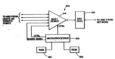
The basic building block or component 100 of the
invention is seen in Figure 2. As shown, the component (which
i~ also referred to as the NMS 464) comprises a
multiplexer/demultiplexer 114, a microprocessor 154 with
~ccompanying RAN 162 and RON 166, and a DSU 116. The DSU is
well known in the art, and is sold by the assignee of the
present application as General Da*aComm, Inc. NMS 510.
Co~ponent 100 is utilized for both the master (host) site and
the remote sites, and as shown in Figure 2 is ge~eric. The
. .
microproce~or 154 controls the multiplexer/demultiplexer 114
according to a program which can be stored in ROM 166. Where
the oomponent 100 is used in conjunction with the master s-ite,
the multipl xer multiplexes data from the host terminals in
accord with control information generally generated by the
microprocessor. However, where the component 100 is used in
con~unction with remote sites, the multiplexer 114 not only
multiplexes data from different terminals together with
W093/0454l 2 1 i. ~ 2 2 ~ PCT/US92/07030
control information, but also multiplexes a guard band which
is described in detail below.
Referring now to Figure 3, additional features of the
non- DSU portion of component 100 are seen in more detail. As
shown, microprocessor 154 is preferably a 68302 microprocessor
package having a 68000 microprocessor and several parallel to
serial and.serial to parallel converters 154b, 154c, 154d.
The multiplexer/demultiplexer 114 is preferably constructed of
several LSIs 114a, 114b, 114c, 114d which are used for various
multiplexer functions well known in the art. -.
The LSI chips are manufactured by the assignee of the
present application and are designated "MAFIA (Multiplexer
Asynchronous FIF0 Interface Adapter) Custom LSI Chip".
Fi ~-e 4 shows a basic block diagram of the NAFIA chip. The
NAFIA LSI can be divided into five main functional blocks:
PLL and Baud Rate Generation (902-912); Aggregate SCC Control
932; Data Path (914, 916, 918, 922, 924, g28, 930); DTE Status
Monitor 920; and Nicroprocessor Control (926).
The PLL and Baud Rate Generation generally includes one
PLL 902 ana two independent tLming chains 908, 910 connected
by routing logic 906. The timing chains may also be driven by
external phase-locked high frequency clocks.
The Digital Phase Lock Loop 902 operates from a.master
clock source of 16.128 MHz which is provided externally and
which may be selectively divided by a timing reference select
904.
The baud rate generators must generate four different
clock~ as selected at the -clock selection circuit 912:
Aggregate Transmit Clock; Channel Transmit Clock; Channel
Receive Clock; and an Independent Supplementary clock.
W093/~ ~I PCT/USg2/0~0~
2116228
The Aggregate Control 932 is the interface with the 68302
multi-protocol processor referred to above. It functions as a
dedicated interface to the serial communication controllers,
SCCl and SCC2 and timers of the 68302.
The Data Path is where the serial user data passes
through the LSI. It performs two main functions: Async to
Sync conversion 916 and V.13 simulated controlled carrier 918.
The Async-Sync Converter 916 inserts or deletes stop bits
to handle overspeed or underspeed situations when input da~a
from the DTE is asynchronous and must be re-synchronized to
the system's internal bit clock.
The V.13 Simulated Controlled Carrier 918 is described in
CCITT recommendation V.13. Serial - Parallel conversion is
provided by 922 and 924 because data is processed by the
multiplexer in eight bit bytes and user data is in serial
form. Part of the conversion requires In and Out FIF0 buffers
928 and 930.
To allow flexible external clocking of transmit data, an
elastic buf*er 914 i8 provided in the data path. The range of
elasticity should be _8 bits and the size of the buffer should
be 16 bit~.
In order to support many diagnostic functions it is
nece~ry that ~ignals at the~DTE be monitored. To
accommodate-this need, activity monitors such as the DTE
Statu~ Monitor 920 shown in Figure 4 are provided. These
monitor~ are es~entially edge triggered latches which will
capture a transition and remain in state until reset by the
microproce~or.
WO 93/04s4l PCr/USg2/07030
2~i6228 -
The MAFIA LSI is designed l~o interface to a
microprocessor through an 8-bit bus 934. The LSI has 15 write
registers and 4 read registers to enable the host
microprocessor to control every function of the LSI circuit.
The MAFIA LSI provides an interrupt request output 926 for
interfacing with the host microprocessor.
The multiplexer is a time division multiplexer which
works with packets of bytes. It has a storage facility and is
programmed according to a frame where packets of bytes are
taken from one source before packets of bytes are taken fr;om
another source.
Figures 5 and 6 show the different start-up procedures
for component 100 when used as master or remote units. During
the start-up procedure, the master and remote units cooperate
in order to permit a measurement of delay.
Referring now to Figure 5, the master unit upon power-up
402 determines if any remotes are installed 404. If not, it
waits for a user command 408 to install the first remote. If
remotes are installed, the master broadcasts an outbound
"Disable Transmitter" co~mand 406 to all remotes. The master
then performs delay measureDIents 410, 412, 414 (described
below) on each remote.
. ~ .
After all delay measurements are made, the master
broadca~t~ an outbound "Enable Transmitter" command 416 to all
remotes and normal user data transmission 418 begins.
Referring now to Figure 6, the remote unit on power-up
502 first di~;ables its transmitter 504 waits for a poll from
the ~a~ter 506. If it does receive a poll from the master, it
respond~ 508 and if the master acknowledges 512, the remote
~nables its transmitter 518 and begins normal operation 520.
If no poll from the master unit is received 506 or if the
WO 93/04541 PCI`/US92/07030
21162~ lo
master does not acknowledge 512 the response by the remote 508
to the master's poll, the remote waits for delay measurement
request 510. If no delay measurement reguest is received 510,
the remote again waits for a poll from the master unit so4.
If a delay measurement request is received from the master
510, delay measurement is performed 514 and the remote waits
for the "enable transmitter' command 516 from the master.
When the command is received, the remote enables its
transmitter 518 and begins normal operation 520.
The delay measurement procedures for the master and
remote units upon power-up are shown in more detail in Figures
8a and 8b, respectively and described below in the discussion
of Propagation Delay Compensation. The delay measurement is
used to provide information about the time delay of the
different remote units so that data sent from the remote units
can be synchronized one relative to the other. Since each
remote site might experience different delay and data from a
plurality of sites is to be time division multiplexed, account
must be made for the delay from each site. As mentioned
above, the basic technique of synchronizing the remote sites
to account for delay is known in the art.
Turning to Figure 7a, the framing of outbound data is
~hown. The outbound frame is assembled in a generally
~tan~a~d manner and i8 preferably 10 msec in length. It
include~ sync and control information in addition to data from
one or more channels. Outbound frames are transmitted
continuou~ly or in what is referred to as "constant carrier
mode". The number of bytes in an outbound frame is determined
by the data rates of the channels. For example, the table
below indicates the number of bytes generated by a channel in
10msec at data rates from 2.4 kbps to 64.0 kbps:
WO g3/04541 ,2: 1 1i6`%,`2 ~ PCr/USg2/07030
11
Data Rate Bits/lOmsec BYtes/lOmsec
2.4k 24 3
4.8k 48 6
7.2k 72 9
9.6k 96 12
12.Ok 120 15
14.4k 144 18
16.8k 168 21
19.2k 192 24
38.4k 384 48
56.Ok 560 70
64.Ok 640 80
If for example, the outbound frame is to eontain data
from 4 ehannels and the data rates of the 4 channels are
9.6 kbps, 2.4 kbps, 2.4 kbps, and 38.4 kbps, the agqregate
data stream must have a rate of 56 kbps. This means that
the outgoing frame may eomprise 70 bytes. The total number
of data bytes is 66: ehannel 1 has 12 bytes per frame,
ehannels 2 and 3 eaeh have 3 bytes and ehannel 4 has 48
bytes. In general, a minimum of 3 bytes are needed for
~ynehronization, Neteon diagnostie and "inband" master-to-
remoté eo D unieation whieh will be deseribed in more detail
below.
The lOm~ee aggregate outgoing frame must be assembled
before it ean be sent. Input buffers for eaeh ehannel
aeeu~ulate the appropriate number of bytes needed for eaeh
frame eyele. With this input~buffer arrangement, it is
elear that all input data ineur a minimum delay of lOmsec
due to the holding time in the buffers. In order to reduce
this buffer delay, the lOmsee frame may be further divided
into tbree equal data segments so that the buffer delay
that any one ehannel will suffer is between 3.33 and
6.67m~ee. Therefore, in the 4 ehannel example above, the
aggregate outgoing frame strueture ean be seen in the table
below:
W093/04~l PCT/US92/07030
21~22~ 12
Byte 1 FRAME sync byte
Byte 2 Netcon/Control BYTE 1 Sync Header
Byte 3 Netcon/Control BYTE 2
Byte 4 Not u~ed
.
Byte 5 Channel 2 data
Byte 6 Channel 3 data
Byte 7 Channel 1 data
Byte 8 Channel 1 data Data Segment 1
Byte 9 Channel 1 data (21 bytes)
Byte lO Channel 1 data ..
Byte 11 Channel 4 data
Byte 12 Channel 4 data . -~:
Byte 25 Channel 4 data
Byte 26 Channel 4 data
Byte 27 Channel 2 data
Byte 28 Channel 3 data
Byte 29 Channel 1 data
Byte 30 Channel 1 data Data Segment 2
Byte 31 Channel 1 data (21 bytes)
Byte 32 Channel 1 data
Byte~33 Channel 4 data
Byte 34 - Channel:4 data
- ~ : -
- -
Byte 47 Channel 4 data,
Byte 48 Channel 4 data
Byte`49 Channel 2 data
Byte 50 Channel 3 data .
Byte 51 Channel l data
Byte 52 Channel 1 data Data Segment 3
By*e 53 Channel 1 data (21 bytes)
Byte 54 Channel 1 data
W093/0454l PCT/US92/07030
2 ~ 8
13
Byte 55 Channel 4 data
Byte 56 Channel 4 data
Byte 69 Channel 4 data
Byte 70 Channel 4 data
It will be appreciated that for channel rates 56 kbps
and 64 kbps, the number of bytes, 70 and 80 respectively,
are not divisible by 3. To maintain the three data segment
division of the frame, one segment may be prearranged to ;
have one byte more than the others. This is not a problem
so long as the demultiplexing scheme does exactly the
reverse.
The multiplexed frame of 70 bytes shown above is one
example. The frame is con~tructed and transmitted
repeatedly. At another aggregate rate, the multiplexed
~rame ~ay take on different organizations.
At the receiving end of such a multiplexed data
stream, the reverse process is performed and the channel
data i~ rea~sembled. In order to perform thi~ process, it
i~ e~enti~l to locate the beginning of each frame. Thus,
a-known 8-bit pattern is sent as the FRANE SYNC byte at the
~tart o~ eNch frame. In the above example, therefore,
FRANE SYNC bytes are separated by 70 bytes or 560 bits. As
i~ known in the art, the receiver circuitry is capable of
performing some form of auto-correlation on the aggregate
signal to obtain synchronization.
,
The FRANE SYNC byte is preferably ¢onstructed so that
the probability that some ~ser data appearing identical to
it frame-after-frame îs sufficiently low. A sample FRAME
8XNC byte is shown in the table below:
w093/04~l PCT/US92/07030
~ ..
~ 14
bit 1 x Modulo-4 counter
bit 2 x incremented once per frame
bit 3 1
bit 4 1 Fixed
bit 5 1 six-bit
bit 6 o pattern
bit 7 o
bit 8 1
In accordance with the invention, it is desirable that
every third outbound frame be designated a Superframe.
Superframes will contain control information for
~ynchronization, Netcon and auxiliary communication as
described in more detail below.
Turning to Figure 7b, the inbound framing is seen.
Because the data contained in the inbound frame is provided
in response to polling, it will be appreciated that the
inbound frame functions according to a "Switched Carrier
Mode".
In any polled application, it is the responsibility of the
ra~ter (control) station that only one tributary ~tation
(remote terminal) respond at any one time. Therefore, it
i~ true to cay that Drop-l channel-1 will always be
inactive while Drop-2 channel-l is responding or vice
ver~a. But with a nu~ber of independent applications
running ~imultaneously, one at each channel, collision
,
between channels (e.g. Drop-l channel-l and Drop-2
ch~nnel-2) is a real possibili~ty.
In order to prevent data collisions, a standard "time-
~licingn ccheme is adopted for the inbound (from remote to
master) aggregate transmission (frame). For example, given
so~é arbitrary time reference tO = 0, a first time slot may
be defined as tO to tl, which can be reserved for responseæ
from channel 1. Similarly, a second time slot tl to t2 can
be re~erved for responses from channel 2, etc, until a
complete cycle is performed allowing for responses from
WOg3/04~1
PCT/US92/07030
each channel. This example is shown more clearly in the
table below:
If one assumes that all inbound propagation delays on
this exemplary multipoint line are identical, then by
arranging all remote drops to adopt the same time-slicing
boundaries, collisions can be avoided.
To establish a common time reference tO among all
remote drops, the outbound signal from the master to the
remotes is used. As mentioned above, the outbound signal
from the master has a frame cycle of lOmsec. All of the
remotes which are receiving the outbound signal, therefore,
may derive a co D on "clock" that ticks once every lOmsec.
Noreover, every one out of X (preferably 3) outbound frames
contains a tag to identify it as a Superframe. At each
remote receiver, Superframe timing information is extracted
to establish the time reference tO for use in the time-
slicing scheme described above.
To ~urther enhance collision protection, adjacent
channel time-slots are separated by gaps, so that minor
~itters of an integer number of bits can be tolerated
without resulting in overlapping of adjacent channel
responses. Such a scheme of gaps is shown for example in
the table below where the gaps are shown with the letter G:
Image
W093/~ ~I PCT/US9~/07030
16
At the receiver of the master multiplexer, the
boundaries of channel time-slots are established using the
master's own transmit signal Superframe timing as
reference.
The gaps between time slots are preferably 3 bytes and 21
bits of those three bytes are designated as the guard band.
As mentioned above, the guard band enhances collision
protection, but also enables the efficient use of "control
mode idle", prevents errors during bit slippage of a remote
port, and provides means for "on-the-fly" correction of
time delay of remote ports.
The guard band is normally 21 marks, i.e. twenty-one
bits, all 1. The remaining 3 bits in the 3 byte gap
distinguish whether the time slot following the gap is the
start, middle or end of a channel response. The first bit
(bit 6 of the third byte) works like a "s,art bit" and is
always set to "0" if there is data present. The second and
third bits (bit 7 and bit 8 of the third byte) are used as
status flags to inform the receiver of the following
conditions:
bit 7 bit 8 The subsequent data carried in this
0 0 ,time-slot is a complete response
0 1 the start of a response
1 0 the middle section of a response
1 1 the end section of a response
These last two bits of thè third byte in the qap are
normally followed by an 8-bit "byte count" at the start of
each time slot which informs the receiver of the length of
the subsequent data stream. When bit 7 = 1 and bit 8 =`0,
however, the byte count can be omitted since it is apparent
that the data stream spans the entire time-slot.
Additional ~byte count" bytes may be needed for high data
rates.
WO93/045~l 2 1 1 ~ 2 2 ~' PCr/USg2~07030
17
It can be seen that the gaps between time-slots
consume bandwidth. To minimize loss and maximize bandwidth
efficiency, therefore, the inbound frame time cycle should
be as long as possible. On the other hand, if the time
cycle of the inbound frame is too long, transaction
response time is increased. A compromised value of 3Omsec
is preferred.
In the four channel example described above with reference
to the outbound frame, a 30msec inbound frame can comprise
1680 bits (56 x 30) or 210 bytes of data. An illustration
of the organization of such an inbound multipoint frame is
shown below where the binary representations in Bytes 3,
24, 36, 48, and 207 are shown LSB first:
Byte 1 FF hex, start of 21-bit guard band
Byte 2 FF hex,
Byte 3 SS011111 bin, 0=start of data, SS are status flags
Byte 4 "Byte Count" or data byte 1
Byte 5 Channel 1 data byte 1 or 2, (4.8 kbps)
Byte 21 Channel 1 data byte 17 or 18
Byte 22 FF hex, start of 21-bit guard band
Byte 23 FF hex,
Byte 24 ~ SS011111 bin, 0=start of data, SS are status flags
Byte 25 "Byte Count" or data byte 1
Byte 26 Channel 2 data byte 1 or 2 (2.4 kbps)
Byte 33 Channel 2 data byte ~ or 9
Byte 34 FF hex, start of 21-bit guard band
Byte 35 FF hex,
Byte 36 SS011111 bin, o=start of data, SS are status flags
Byte 37 "Byte Count" or data byte 1
Byte 38 Channel 3 data byte 1 or 2 (2.4 kbps)
Byte 45 Channel 3 data byte 8 or 9
wos3/04~l PCT/US92/07030
~ 18
Byte 46 FF hex, start of 21-bit guard band
Byte 47 FF hex,
Byte 48 SS011111 bin, o=start of data, SS are status flags
Byte 49 "Byte Count" or data byte 1
Byte 50 Channel 4 data byte 1 or 2 (38.4 kbps)
Byte 192 Channel 4 data byte 143 or 144
Byte 193 FF hex, 6 more bytes of marks reserved for use as
: : "gaps" for two or more additional channels
Byte 198 FF hex
Byte 199 Not used, (1.6k of bandwidth is not used)
Byte 204 Not used
Byte 205 FF hex, start of 21-bit guard band
Byte 206 FF hex,
Byte 207 SS011111 bin, 0=start of data, SS are status flags
Byte 208 Control/Diagnostic Channel data byte 1
Byte 209 Control/Diagnostic Channel data byte 2
Byte 210 Control/Diagnostic Channel data byte 3
Figure 7b shows this arrangement of the inbound data
frame in a ~chematic way and also shows an additional control
channel C sent at the end of each frame. In the frame
described above, the control channel is the last 3 bytes of
the frame (Bytes 208-210 in th~ table above). The control
channel, like the data channels, is bracketed with gaps
including guard bands. The control or diagnostic data time
slot shown in Figure 7b may be used as shown in the flow chart
of Figure 9 (which is discussed in detail below) to monitor
delay while data is being sent.
WO 93/~1 2 1 ~ 6 2 2 8 PCT~US92/07030
19
In a real network, propagation delays will be different
from drop to drop. These delays must be "equalized" in order
for the signals to be synchronized. Equalization i8
accomplished by a circuit initialization procedure during
which each remote drop is polled and propagation delay is
measured. The measured values are then sent back to each
remote for adjusting the time reference tO. The flow charts
in Figures 8a and 8b show this procedure generally.
Turning now to Figures 8a and 8b, the master first at 602
broadcasts a command to disable al~ remotes (hold mark) and
then at 604 waits a reasonable time for all remotes to acquire
frame synchronization. the remotes receive the disable
transmitter command at 622 and disable their transmitters at
624. Next at 606, the master sends a "prepare for delay
measurement" co D and to a specific remote and waits until the
transmission of the next Superframe to start a counter at 608
which is clocked by the aggregate TX clock. Then the master
waits at 610 for the remote response. Meanwhile, the remote
at 626 receives the "prepare for delay measurement" or if none
is received, enables its transmitter at 634. After receiving
the Hprepare for delay measurement" at 626, the the addressed
remote at 628 waits for the next Superframe sync pattern.
When the Superframe sync pattern is detected, a response is
i D ediately sent back to the master which receives it at 610.
If no response is received by the master at 610, the master
broadcast~ an enable transmitter command to all remotes at
618. If the master receives the response from the remote at
610, the master stops the counter at 612 and records the count
on the counter and calculates the delay equalization value for
the specific remote at 614.
The count is proportional to the round-trip propagation
delay for the ~elected remote drop. Based on the measured
value, the master at 616 s~nds back to the remote a Delay
Egualization Count which may have the value
N - Count, if Count S N or,
2N - Count, if Count S 2N or,
3N - Count, if Count 5 3N or, etc.
WO93/04~l PCT/USg2/07030
~116~2~ 20
where N = (3 x Aggregate Speed)/100. The value 3 is used here
assuming that there is one Superframe for every 3 frames.
This is a good value to use since it represents an optimized
compromise between Available User Bandwidth and Response Time.
The number of Superframes may be different, however, under
different circumstances.
The selected remote then receives at 630 the Delay
Equalization Count, delays its current time reference tO by
that amount, and waits at 634 for the enable transmitter
command from the master. If the remote does not receive a
Delay Equalization Count at 630, it suspends normal data
transmission and waits at 632 for the next delay measurement.
The master repeats the steps at 606 through 616 for each
remote and then broadcasts at 618 an "Enable Transmitter" and
begins normal operation at 620.
E~ch remote, after receiving the "Enable Transmitter" at
634 proceed to normal data transmission at 636. If a remote
does not receive an "Enable Transmitter" command at 634, it
waits at 626 for a "prepare for delay measurement" command
from the master.
The procedure i8 carried out when the master i8 first
powered on or when a new remote drop is being installed. It
can al~o be initiated by a command from the Netcon controller.
The control channel discu~sed above and shown schematically in
Figure 7b can al~o be used to permit a substantially
continuous monitoring of propa`gation delay so that remote
terminals can be adjusted and kept in sync.
Figure 9 shows a flowchart of how the master monitors the
propagation delay of the remote units and adjusts the
transmitter off~et of the remote units to compensate for
change in delay. The master unit at 704 polls the first
remote and sets a timer to measure the arrival time of the
response from the first remote. The master also starts a
wo 9~,04541 2 I 1 6 2 2 $ PCI /US!~2/1~7030
time- out timer at 706. If no response at 708 is received
from the first remote within the time-out interval at 710, the
master skips to the next remote at 718. If a response is
received at 708 before time-out at 710, the master calculates
at 712 whether the arrival time is less than 5 bits (five
aggregate clock periods) different from the nominal time
associated with the first remote. If the arrival time is
within 5 bits of the nominal time, the master at 714 sends a
"good" acknowledgement to the first remote. If the arrival
time is more than 5 bits different (either earlier or later)
than the nominal time, the master at 716 orders the first
remote to shift its transmitter offset to compensate for the
change in delay. The master then at 718 repeats this
procedure for all remotes.
This monitoring is slow but substantially continuous and
it pro ides enough protection so that a determination can be
made and corrective action taken before the system needs to be
shut down due to errors.
The correction command is sent to the remote unit in the
control information section of the outbound frame. Correction
is not made unless the difference between the measured and
nominal values of Tl is significant (preferably > 5 bits)
since small differences may be the result of a temporary
glitch and not require corrective action.
As mentioned above, the outbound frame includes two
control bytes in its header. ~hese bytes are preferably
constructed according to the table below:
wos3/04~l PCT/US92/07030
21~2~ 22
BYTE 1:- Status Flags
bit 2 - 1, (21)
oo = Not a Superframe
01 = Superframe A
10 = Superframe B
11 = Superframe C
bit 3, Not used
bit 6 -4, (654)
000 = Next byte is Netcon data
001 = Next byte is Aux. Ch data
011 = Next byte is Ctl data
101 = Next bvte is Start of Ctl data
110 = Next byte is End of Ctl data
bit 7, 0 = Unit is a Diagnostic Remote, as set by DSU
1 = Unit is a Diagnostic Master, as set by DSU
bit 8, 0 = Expects Constant Receive Carrier
1 = Expects Switched Receive Carrier
BYTE 2:- Netcon, Aux'y Channel or Control data
The first byte is used as a status indicator. It
~peoi~ies whether the second byte~is Netcon data, Auxiliary
Channel data, or Control data~and it indicates whether the
current frame is a Superframe. In the case of a Superframe,
~tatus bits are also assigned to distinguish if it is a
Superframe A, Superframe B, or Superframe C. The distinction
is~required to coordinate the inbound responses from the three
separate sources mentioned above. Bit 7 indicates to the
remote receiver, the unit's master/remote status as told by
its DSU. Bit 8 lets the remote receiver know what receive
carrier mode this unit expects. For example, if the remote
WO 93/04541 PCI~/US92/07030
21i.6~
23
receiver is to be used in a point to point mode, bit 8 is set
to 1. However, for purposes of this invention, bit 8 is set
to 0, as a constant carrier is expected from the master.
Since each outbound frame carries only one byte of control
data, a complete command may span a number of outbound frames
and errors may be detected through the use of a checksum byte.
Three bytes are available for inband communication in the
30msec inbound frame. These bytes are preferably constructed
according to the table below:
BYTE 1:- Status Flags.
bit 3 - 1, (321)
000 = Next byte is a Netcon character
001 = Next two bytes are Netcon char's
010 = Next byte is Aux'y Channel data
011 = Next two bytes are Aux Channel data
100 = Next byte is Control data.
101 = Next two bytes are Control data.
bit 8 - 4, Not assigned
BYTE 2:- Netcon, Auxiliary Channel or Control data
BYTE 3:- Netcon, Auxiliary Channel or Control data
The master normally addresses each remote by its Drop
Number. Responses from the remote to the master are always
two bytes at a time.
As will be appreciated,-the guard band is a critical
~spect o~ this invention. During the guard band, the remote
DSUs can inform the OCUs to which they are coupled whether
they will be sending data or not in the time slot following
the guard band. m is information is then used by the OCU to
inform tbe NJU of the same so that the NJU can shut off the
OCU data input to the MJU if the OCU is not sending data. In
this manner, the "data mode idle~ discipline is avoided and
the syctem i~ not susceptible to noise. By sending the
"control mode idle" command in the guard band (as well as in
W093/0454l Pcr/US92/07~30
21~2X 24
the non-data carrying time-slot following the guard band), any
lagging response by the OCU can be compensated for. Noreover,
the guard band also guards against errors which would
otherwise result from a change in the delay from a remote
terminal to the master. With the guard band, should data from
one OCU be received slightly earlier or later than expected,
it will not conflict with data from another remote terminal.
In other words, the untimely OCU will, because of the guard
band, begin transmission with 21 bits of marks (the guard
band) and will simply put the untimely OCU from control mode
idle into data mode idle. If data is received during the
transmission of a guard band, signaling that delay from a
remote terminal has changed, the master microprocessor will
determine that there has been a change. Furthermore, as
previously described, the system is provided with monitoring
means in the control signalling in order to determine which
remote terminal has changed its delay.
There have been described and illustrated herein digital
multiport multidrop systems. While particular embodiments of
the invention have been described, it is not intended that the
invention be limited thereby, as it is intended that the
invention be as broad in scope as the art will allow. Thus,
it is understood by those skilled in the art that while a
guard band has been described as preferably having twenty-one
bits, it will be appreciated that a guard band having a
different number of bits can be used, provided there is enough
time for the DSU to communicate to the OCU (and the OCU to the
MJU) that no data will be sent from that DSU during the next
slot in the frame. Also, while particular hardware and
software arrangements have been provided, it will be
appreciated that one, the other, or both can be suitably
changed, but will still provide the same guard band,
monitoring, and other functions. Therefore, it will be
appreciated by those skilled in the art that yet other
modifications could be made to the provided invention without
deviating from its spirit and scope as so claimed.