Note: Descriptions are shown in the official language in which they were submitted.
2116995
- 5260-41
THREE-T~MTN~T CAPACITOR AND A88EMBLY
BACRGROUND OF THE lNV~. ~ ION
1. Field of the Invention
This invention relates to a three-terminal type capacitor, a
three-terminal type capacitor array, and an assembly for removing
jamming signals incorporating the three-terminal capacitor and/or
array. The capacitor and capacitor array of this invention are
suited for removing jamming signals generated by the electric
circuit which includes the capacitor or jamming signals received
from other electric circuits, such as in electrical appliances
like television sets.
2. Description of the Prior Art
Recently, as digital circuits in electrical appliances
become smaller in size and greater in function the parts used in
them for removing jamming signals must also be smaller in size
and have a superior ability to remove jamming signals. As a
representative example of prior art systems for removing jamming
signals, the assembly of FIG. 1 shows a disk-shaped feed-through
capacitor 5 comprising a signal electrode 1, a dielectric 2, and
a ground electrode 3. As shown in FIG. 2, feed-through capacitor
5 is attached to the input/output terminals of a metal shield
case 4 incorporating electric circuits.
In this type of conventional jamming signal removal device,
the spacing of signal lines is determined by the size of the
feed-through capacitor 5. Therefore, when the number of signal
lines increases the number of feed-through capacitors 5 contained
in the metal shield case 4 increases and the size of the jamming
signal assembly becomes very large. Further, the manufacturing
efficiency of the jamming signal assembly is reduced due to the
increased number of feed-through capacitors because each feed-
211699S
t~rough capacitor 5 must be individually soldered to metal shieldcase 4.
Japanese Patent Publication No. 4-32170, represented by the
drawing of FIG. 3, discloses a reduced size assembly for removing
jamming signal comprising a terminal strip mounting a printed
type capacitor on a metal shield case. The terminal strip is
made by sequentially forming a first electrode layer 12, which is
a ground electrode of the capacitor, on a ceramic substrate 11
having a penetration hole 15, and a dielectric layer 13. A
second electrode layer 14 is soldered on dielectric layer 13 and
around penetration hole 15, and a pin terminal 16 is inserted
into the penetration hole 15. The terminal strip is fixed in a
metal shield case (not shown) by a protrusion 17 of the metal
shield case. Although the terminal strip of FIG. 3 can be
reduced in size, the performance of jamming signal removal is
reduced because the dielectric layer 13 is not wrapped in first
electrode layer 12 structurally.
The devices described above provide important advantages in
operation. Nevertheless, none of these devices provide the
important advantage of both superior jamming signal removal in a
small size assembly.
8UMMARY OF THE lNv~..lON
According to this invention, a reduced size three-terminal
type capacitor is provided for removing jamming signals from an
electrical signal. The three-terminal type capacitor comprises a
ceramic substrate with a first ground electrode layer formed on
the ceramic substrate and a first dielectric layer formed on the
first ground electrode layer. On the first dielectric layer
extending at least from one end of the first dielectric layer to
the other end is a signal electrode. A second dielectric layer
is formed on the first dielectric layer to surround the signal
electrode together with the first dielectric layer, and a second
ground electrode layer is formed on the second dielectric layer
together with the first ground electrode layer. The second
ground electrode layer is electrically connected to the
first ground electrode layer. The first and second ground
electrode layers have different thicknesses.
In another embodiment of this invention, a reduced
size three-terminal type capacitor array removes jamming
signals from electric circuits. The three-terminal type
capacitor array is characterized by disposing a plurality
of the three-terminal capacitors of this invention on a
ceramic substrate and connecting at least one of the first
ground electrode layer and second electrode layer in one
three-terminal type capacitor and at least one of the first
ground electrode layer and second ground electrode layer in
another three-terminal type capacitor.
Furthermore, this invention provides an assembly for
removing jamming signals characterized by using an
insulating substrate to form a first conductive pattern for
grounding and a second conductive pattern for grounding
electrically connected to the first conductive pattern on
the surface of the insulating substrate. As least one of
either the three-terminal type capacitor and/or three-
terminal type capacitor array are mounted on the first
conductive pattern of the insulating substrate, and at
least one of the first ground electrode layer and second
ground electrode layer of the three-terminal type capacitor
and/or three-terminal type capacitor array is electrically
connected to the first conductive pattern of the insulating
substrate. A metal shield case is then fixed to the
insulating substrate so that the second conductive pattern
of the insulating substrate and the bottom end of the metal
shield case make contact with one another.
Additionally, this invention provides a method of
making a three-terminal type capacitor or three-terminal
type capacitor array. The method of making a three-
terminal type capacitor comprising the steps of forming a
ceramic substrate and forming a first ground electrode
layer on the ceramic substrate. 'On the first ground
_ electrode forming a first dielectric layer having two ends
followed by a signal electrode extending at least from one
end of the first dielectric layer to the other end. A
second dielectric layer is then formed on the first
dielectric layer to surround the signal electrode together
with the first dielectric layer, and a second ground
electrode layer is formed on the second dielectric layer to
surround the first dielectric layer and second dielectric
layer together with the first ground electrode layer, the
lo second ground electrode being electrically connected to the
first ground electrode, where the first and second ground
electrode layers have different thicknesses.
The method of making a three-terminal type capacitor
array is similar to the method of the making the three-
terminal type capacitor, except that a plurality of three-
terminal type capacitors are formed on the ceramic
substrate and are then electrically connected through at
least one of the first ground electrode layer and the
second ground electrode layer in one three-terminal type
capacitor and at least one of the first ground electrode
layer and second ground electrode layer in another three-
terminal type capacitor.
As pointed out in greater detail below, the three-
terminal type capacitor of this invention provides greater
advantages over the above prior art devices. The three-
terminal type capacitor and three-terminal type capacitor
array are of a laminar structure wrapping the dielectric
layer with the ground electrode layer, and therefore
provide the important advantages of a thin structure and
excellent jamming signal removal performance. In
particular, by varying the thickness of the first ground
electrode layer and thickness of the second ground
electrode layer, the potential difference between the two
ground electrode layers due to high frequency components
can be eliminated and excellent jamming signal removal
performance achieved.
.
211699~
_
The assembly for removing jamming signals mounting the
three-terminal type capacitor and/or three-terminal type
capacitor array is excellent in improving jamming signal removal
performance, and the spacing of signal lines can be narrowed so
that the size of the assembly can be reduced. In particular, in
the assembly electrically connecting the connection member of the
three-terminal type capacitor array and the first conductive
pattern of the insulating substrate suppresses the generation of
crosstalk occurring when the spacing of the signal lines is
narrowed.
The invention itself, together with further objects and
attendant advantages, will best be understood by reference to the
following detailed description taken in conjunction with the
accompanying drawings.
BRIEF DEBCRIPTION OF THE DRAWINGB
FIG. 1 is a perspective view of a conventional feed-through
capacitor.
FIG. 2 is a perspective view of a conventional assembly for
removing jamming signal incorporating the feed-through capacitor
of FIG. 1.
FIG. 3 is a perspective exploded view of a terminal strip
including a conventional printed type capacitor.
FIG. 4 is a perspective view of the preferred embodiment of
a three-terminal type capacitor of this invention.
FIG. 5 is a sectional view along line A-A of FIG. 4.
FIG. 6 is a sectional view along line B-B of FIG. 4.
FIG. 7 is a cross sectional view of an alternative
embodiment of a three-terminal type capacitor of this invention.
FIG. 8 is a perspective view of a three-terminal type
capacitor array of this invention.
FIG. 9 is a sectional view along line C-C of FIG. 8.
FIG. 10 is a perspective exploded view of an assembly for
removing jamming signals having a three-terminal type capacitor
2116995
array mounted on a printed circuit board in accordance with this
invention.
FIG. 11 is a perspective exploded view of an assembly for
removing jamming signal having a three-terminal type capacitor
array mounted on a multilayer printed circuit board in accordance
with this invention.
DE8CRIPTION OF THE PREFERRED EMBODIMENT8
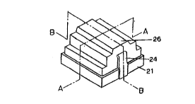
Turning now to the drawings, FIG. 4 shows the overall view
of a first embodiment of the three-terminal capacitor of this
invention and FIGs. 5 and 6 represent sectional views of the
three-terminal capacitor along lines A-A and B-B, respectively.
The three-terminal capacitor of this invention is of a laminar
structure and comprises a first ground electrode layer 22 formed
on a ceramic substrate 21 and a first dielectric layer 23 formed
on first ground electrode layer 22. A signal electrode 24,
formed in the middle of first dielectric layer 23, is covered by
a second dielectric layer 25 formed on first dielectric layer 23
and signal electrode 24. A second ground electrode layer 26
surrounds a second dielectric layer 25 so that both ends of
second dielectric layer 25 contact and communicate with the first
ground electrode layer 22.
As shown in FIG. 4, the signal electrode 24 extends from one
side of the ceramic substrate 21 to the other end of the ceramic
substrate 21 above the first dielectric layer 23. In the
preferred embodiment, each layer of the three-terminal capacitor
is formed by using thick film printing technology where the
capacitor is produced by printing the electrode layer on the
ceramic board and sintering the electrode layer and then printing
and sintering the dielectric layer. Another suitable method to
produce the invention uses dielectric green sheets instead of
printing the dielectric layers or the various layers of the
three-terminal capacitor can be formed by printing electrode
layers and dielectric layers alternately and then sintering them.
' 211699~
Unlike the conventional printed type capacitor, the
structure of three-terminal type capacitor is such that the first
and second dielectric layers 23 and 25 are surrounded by mutually
conducting first and second ground electrode layers 22 and 26.
By surrounding the dielectric layers with the electrode layers,
the inductance of the capacitor is reduced. Therefore, the high
frequency performance of the capacitor is improved and the
assembly incorporating the capacitor has superior ability to
remove jamming signals.
In an alternative embodiment shown in FIG. 7, the three-
terminal type capacitor comprises a second ground electrode layer
27 which is thicker than first ground electrode layer 22. Second
ground electrode layer 27 is of variable thickness with its
thickest point being above second dielectric layer 25.
In a flat capacitor as shown in FIG. 4, a high frequency
current flows from first and second dielectric layers 23 and 25
into first and second ground electrode layers 22 and 26. When
this high frequency current is flowing in first and second ground
electrode layers 22 and 26, if the first ground electrode layer
22 is connected to an external ground terminal, the impedance of
the second ground electrode layer 26 further from the external
ground terminal is slightly larger than the impedance of the
first ground electrode layer 22. Accordingly, a potential
difference exists between first ground electrode layer 22 and
second ground electrode layer 26, thus lowering the performance
of the three-terminal capacitor.
On the other hand, in the embodiment of FIG. 7, when the
second ground electrode layer 27 is of a thickness greater than
the first ground electrode layer 22, the impedance of the second
ground electrode layer 27 decreases. Accordingly, when a high
frequency current flows, the impedance is balanced between first
ground electrode 22 and second ground electrode 27, and
generation of a potential difference between first and second
2116995
g~Found electrode layers 22 and 27 is suppressed. Therefore, when
the first ground electrode layer 22 is connected to an external
ground terminal, it is preferable to use a second ground
electrode layer 27 that is thicker than the first ground
electrode layer 22 to achieve even greater jamming signal removal
performance.
In yet another variation depicted in FIGs. 8 and 9, a three-
terminal type capacitor array comprises a first ground electrode
layer 32 formed on a ceramic substrate 31. Two first dielectric
layers 33 are formed on first ground electrode layer 32, and each
first dielectric layer 33 has a signal electrode 34 formed in the
middle thereon. Two second dielectric layers 35 are formed on
first dielectric layers 33 to cover each signal electrode 34. A
second ground electrode layer 36 is formed to cover second
dielectric layers 35 and to contact and communicate with first
ground electrode layer 32. Each signal electrode 34 extends from
one side to the other of the ceramic substrate 31 (i.e.
perpendicular to line C-C) above each first dielectric layer 33.
Alternating with signal electrodes 34, on the side of ceramic
substrate 31, are ground terminal parts 37 which extended from
the second ground electrode layer 36. In this embodiment, each
layer of the three-terminal type capacitor array is formed by
employing thick film printing technology. However, any other
suitable method known to those skilled in the art can be used.
In yet another variation, the three-terminal type capacitor
array of FIG. 8 can be incorporated in an assembly for removing
jamming signals as shown in FIG. 10. The assembly of FIG. 10
comprises a printed circuit board 41 with a three-terminal type
capacitor array 47 disposed near the input and output unit of the
printed circuit board 41. A metal shield case 48 fits over the
printed circuit board 41 such that the entire board including the
three-terminal type capacitor array 47 is covered.
2116995
.,.
In the preferred embodiment, the etching method is used to
place a first conductive pattern 42 and a signal lead-out pattern
44 on the surface of printed circuit board 41. First conductive
pattern 42 is for grounding and comprises a terminal connection
part 43 for connecting the ground terminal of the three-terminal
type capacitor array with ground. The signal lead-out conductive
pattern 44 conducts the signal from an electric circuit (not
shown in FIG. 10) disposed on the printed circuit board 41 to the
three-terminal type capacitor array 47 by connecting with the
signal electrode of the three-terminal type capacitor array 47.
on the surface of the printed circuit board 41, an insulator
layer 45 is formed across and above the signal lead-out
conductive pattern 44. A second conductive pattern 46 is formed
on the insulator layer 45, and serves as a ground and contacts
the bottom end 49 of the metal shield case 48. The signal lead-
out pattern 44 is positioned below the second conductive pattern
46, and is separated from the second conductive pattern by the
insulator layer 45. Both ends of the second conductive pattern
46 are soldered to the first conductive pattern 42.
The above described structure provides superior ability to
closely connect the bottom end 49 of the metal shield case 48 and
the second conductive pattern 46. Further, it is easier to
fabricate the metal shield case 48 and the printed circuit board
41. If the signal lead-out pattern 44 were positioned above the
second conductive pattern 46, another insulator member would have
to be placed between the signal lead-out pattern 44 and the
bottom end 49 in order to insulate them. Therefore, the
structure of FIG. 10 provides superior connection and
fabrication.
The three-terminal type capacitor array 47 is mounted on the
first conductive pattern 42 at a position adjacent to the signal
lead-out pattern 44, and the ground terminal part and signal
electrode of the three-terminal type capacitor array 47 are
21 16995
respectively connected to the terminal connection part 43 and the
signal lead-out conductive pattern 44. In the preferred
embodiment, the three-terminal type capacitor array 47 is mounted
using a method of passing a reflow oven after applying cream
solder. However, other suitable methods known to those skilled
in the art can be used.
After mounting the three-terminal type capacitor array 47 on
the printed circuit board 41, metal shield case 48 with an open
bottom end 49 is mechanically attached to printed circuit board
41 so that bottom end 49 and second conductive pattern 46 contact
each other. Bottom end 49 of metal shield case 48 is folded over
like a spring to enhance the contact and electric conductivity
between the bottom end 49 and second conductive pattern 46.
In order to remove jamming signals from an electric circuit,
the three-terminal type capacitor array of FIG. 10 conducts a
signal from an electric circuit (not shown) on the printed
circuit board 41 to the signal electrode 34 of the three-terminal
type capacitor array 47. This signal includes the both the
jamming signal and the original signal. The frequency of the
jamming signal is usually different from that of the original
signal. When the jamming signal passes the three-terminal type
capacitor array 47, it goes to the first conductive pattern 42
through the ground terminal part 37. The apparent filter
matching the frequency of the jamming signal is composed of
capacitance of the three-terminal type capacitor array 47 and
impedance of the electric circuit, and the jamming signal is
attenuated by this filter, thus causing the three-terminal type
capacitor array to remove the jamming signals. Once the jamming
signal is removed, the signal is conducted to the signal lead-out
conductive pattern 44.
This assembly utilizing the three-terminal type capacitor
array provides a thin device with excellent performance in
removing jamming signals. Moreover, since the ground terminal
-- 10 --
211G995
p~rt disposed between signal electrodes of the three-terminal
type capacitor array 47 is directly connected to terminal
connection part 43 of first conductive pattern 42 generation of
crosstalk is suppressed. Further, the number of elements
comprising the a~ssembly is small, thus, manufactur'e using
soldering by a reflow oven is feasible.
As discussed above, the three-terminal type capacitor array
can be used in an assembly for removing jamming signals, as can
the various embodiments of the three-terminal type capacitor.
However, it is easier to incorporate the three-terminal type
capacitor array in an assembly than a plurality of three-terminal
capacitors because where the gap between the signal electrodes is
narrow, crosstalk is likely between the signal electrodes when
three-terminal type capacitors are used as opposed to three-
terminal type capacitor arrays.
Further, if the gap between the signal electrodes is verynarrow, crosstalk is likely to occur between signal lines in a
printed circuit board mounting the three-terminal type capacitor
or three-terminal type capacitor array. However, by connecting
the ground electrode pattern of the printed circuit board and
ground terminal parts 37, generation of crosstalk between the
signal lines can be suppressed. Thus, in the assembly for
removing jamming signals, particularly where the spacing of the
signal electrodes is narrow, it is preferable to use the three-
terminal type capacitor array.
In yet another variation depicted in FIG. 11, a multilayerprinted circuit board 51 having an internal conductive pattern
can be used in an assembly for removing jamming signals. On the
surface of a multilayer printed circuit board 51 is a grounding
conductive pattern 52. Grounding conductive pattern 52 is made
by integrally forming a first conductive pattern 53, mounted with
a three-terminal type capacitor array 47; a terminal connection
part 54, to be connected to the ground terminal part of the
-- 11 --
2116995
t~ree-terminal type capacitor array 47; and a second conductive
pattern 55, to tightly contact the bottom end 49 of metal shield
case 48. Furthermore, on the surface of multilayer printed
circuit board 51, a first signal lead-out pattern 56 connected to
the signal electrode of the three-terminal type capacitor array
47 and a second signal lead-out pattern 57 connected to an
external circuit do not contact the second conductive pattern 55.
On the other hand, inside of the multilayer printed circuit
board 51, a signal lead-out conductive path 58 is provided
beneath second conductive pattern 55 and both ends of signal
lead-out conductive path 58 are connected to a through-hole 59.
The first signal lead-out pattern 56 and second signal lead-out
pattern 57 are electrically connected by way of through-hole 59
and signal lead-out conductive path 58.
The assembly using the multilayer printed circuit board 51,
the three-terminal type capacitor array 47, and metal shield case
48, can be manufactured using the reflow method or any other
suitable method known to those skilled in the art.
Variations of the embodiments described above are possible.
For example, in the three-terminal type capacitor array shown in
FIG. 8, two capacitors are shown, but three or more capacitors
may be formed on the array as needed. Additionally, the
assemblies shown in FIGs. 10 and 11 show two three-terminal type
capacitor arrays, but one or three three-terminal type capacitors
may be used or a mixture of three-terminal type capacitors and/or
three-terminal type capacitor arrays may be used. Further, FIG.
10 shows an example using one-sided printed circuit boards, but
two-sided printed circuit boards may also be used.
The embodiments of the invention described above provide a
number of significant advantages. By using a three-terminal type
capacitor of this invention, first and second conductive layers
(i.e. dielectric layers) are surrounded by mutually conducting
first and second electrode layers so that jamming signal removal
' 211699~
,.~
is superior to that of the conventional printed type capacitor.
Further, in the assembly incorporating the three-terminal type
capacitor or array, electrically connecting the connection member
of the three-terminal type capacitor array and the first
conductive pattern of the insulating substrate suppresses the
generation of crosstalk occurring when the spacing of the signal
lines is narrowed, thus keeping the size of the jamming signal
removal assembly small. Finally, because the size of the
assembly is small, the solder reflow method of manufacture can be
used, thus increasing manufacturing efficiency.
Of course, it should be understood that a wide range of
changes and modification can be made to the preferred embodiments
described above. It is therefore intended that the foregoing
detailed description be understood be regarded as illustrative
rather than limiting and that it be understood that it is the
following claims, including all equivalents, which are intended
to define the scope of this invention.
- 13 -