Note: Descriptions are shown in the official language in which they were submitted.
2117~ 6~
'TITLE OF INVENrION
Multi-cell Battery Monitoring System With Single Sensor Wire.
FIELD OF INVENTION
The present invention relates to a muti-cell monitoring system for
detecting the condition of individual cells within a serially connected bank of
batteries.
BACKGROUND OF THE INVENTION
It is known that the condition of a bank of serially connected
battery cells is dependent upon the condition of the individual cells within thebank. In order to detect a deteriorating one of the cells the condition of a given
cell must be measured individually or as part of a plurality of different groupsof cells. In particular, to monitor battery voltages, it has been common to use a
differential multiplex method in which flying capacitors or high voltage
multiplexes are used to collect voltage from different cells. In either case, atleast one wire per measured cell has been used to provide a sensing voltage for
the multiplexing circuitry. The disadvantage of such a system lies mainly in
- the number of sensing wires.
United States Patent No. 5,099,211 permits measurements of
multi-cell arrangements with a single sensing wire. According to this patent
one lead of a single voltage response switch is connected to each of the inter-
connecting battery termin~ and a common terminal. In addition, the switch
is connected between this common terminal and one of the end termin~l~ of
the bank of batteries. A ramp voltage is then applied between the other end
terminal and the common terminal, the ramp voltage being such as to extend
from zero to a voltage in excess of the total voltage of the bank of batteries. As
the voltage is ramped up each switch is opened then closed, in succession.
This arrangement gives rise to current pulses and both ramp voltage and
instantaneous current through this arrangement are coordinately provided as
output. The voltage between discrete pairs of pulses are an indication of the
-2- 2117166
cell voltage.
A serious drawback of the invention disclosed in United States
Patent No. 5,099,211 is that it is difficult to accurately measure voltages below a
few volts due to the nature of the switching. The method is also noise sensitive5 and might have problems in proper operation in the presence of a ripple
voltage. Furthermore, it employs a rather complicated switching circuit
which has to be built into every battery sensing wire connector.
It is an object of the present invention to provide a multi-cell
battery monitoring system, method and apparatus ut.ili~ing a single sensing
10 wire which is capable of accurately measuring voltage, including voltages
below one volts, in a manner which is resistant to noise and the effects of a
ripple voltage.
Further and other objects of this invention will become apparent to
a man skilled in the art when considering the following summary of the
15 invention and the more detailed description of the preferred embodiments
illustrated herein.
SUMMARY OF THE INVENTION
According to one aspect of the invention there is provided an apparatus
for monitoring the condition of individual cells within a serially connected
20 multicell battery system comprising:
a battery assembly including a plurality of batteries connected in
series;
a plurality of reference terminals including first and second
reference terminals located at the beginning and end of the batteries assembly,
25 respectively, and a plurality of intermediate reference terminals each
interconnecting a plus (+) terminal of a respective one of said batterys to the
negative (-) terminal of an adjacent one of said batterys;
a common sensing lead;
a plurality of voltage and/or current responsive non-linear
- 3 - ~ 6
component switching means, each intermediate terminal and the second
reference terminal being connected to said common sensing lead through a
respective one of said non-linear component switching means, the non-linear
component switching means cooperatively adapted to serially effect a change in
5 the state of each of the respective non-linear component switching means in
response to a predetermined voltage/current present at said common sensing
wlre;
voltage/current generating means for supply to said common
sensing wire a predetermined voltage/current;
means for detecting a change in impedance of said common sensing
wire;
means for instantaneously measuring the voltage and/or current
and/or impedance of said common sensing wire upon detection of said rapid
change of impedance.
means for providing output indicating the condition of at least a
deteriorating one of said individual batteries based on the instantaneous
voltages and/or currents and/or impedances measured. Preferably said non-
linear component switching means sensors are a capacitor and a series
connection of a diode and a resistor. In one embodiment said voltage/current
20 - generating means is capable of injecting into said common sensing wire a
continuous series of incrementally increasing voltages/currents of
predetermined range of magnitude and polarity. In another embodiment said
voltage/current generating means is a RC network connected to a discharge
switch.Preferably said non-linear component switching means further~5 comprises: a MOSFET connected in series with the diode and resistor, the
MOSFET located proximal to the common sensing wire for receiving a
voltage/current impulse from the voltage/current generating means; and
a capacitor connected in parallel between the MOSFET gate an
4 ~117 166
~source and resistor for receiving a charge through an internal diode of the
MOSFET and supplying a voltage to the gate of the MOSFET;
the components of the non-linear component switching means
cooperating to allow serial conduction through a single MOSFET at a time
5 beginning with the MOSFET located to the second reference terminal. In anotherembodiment said non-linear component switching means further comprises a
second diode operatively connected to the MOSFET for limiting the voltage
applied to the gate. Preferably said second diode is a Zener diode. In another
embodiment said non-linear component switching means further comprises a
10 speed up diode placed across the resistor to assist in charging the capacitor.
Preferably said output is in human readable form. In another embodiment said
output includes a voltage reading of each of the individual batteries.
According to yet another aspect of the invention there is provided a
method for detecting the condition of the individual cells of a bank of serially15 connected battery cells using a single common sensing wire connected through
respective non-linear component switching means to respective reference
terminals located between adjacent batteries and at the end of the battery
assembly, which method comprises:
injecting into the common sensing wire a voltage or current of
20 magnitude, polarity and duration sufficient to serially alter the common state of
the respective switching means;
detecting an instantaneous rapid change of impedance at points of
transition of the sate of the individual switches;
determining the voltage and/or current of the common sensing
25 wire at the points of rapid change of impedance; and
providing output indicating the condition of at least a deteriorating
one of said individual batteries based on the voltage and/or current determined
at the points of rapid change of impedance. In one embodiment the voltage or
current injected into the common sensing wire includes a small AC ripple at a
~5~ 211~ 1~ 6
~requency gréater t~Lan the frequency of the serial transition of said switches and
the change in impedance, for example the point of opening of said switches,
being monitored by synchronous detection of the non-injected parameter with
double frequency to detect even harmonics of injected frequency. Preferably the
5 detection of instantaneous change in impedance of the common sensing wire is
accomplished by including the impedance in the resonant circuit of an oscillatorand detecting the change in the free-running oscillation frequency of the circuit
attributable to changes in the impedance. In another embodiment the
instantaneous rapid change in impedance is detected by monitoring the changes
10 in voltage and current in the common sensing wire during the period over
which the respective switches are opened, plotting the change in voltage relative
to change current for that period and comparing the plot against a reference plot.
According to yet another aspect of the invention there is provided a
in combination:
a pair of first and second termin~
a battery assembly connected between said termin~l~ comprising
a plurality of serially arranged batteries having a pair of plus and minus
battery termin~
a plurality of intermediate terminals each interconnecting a plus
20 terminal of one said batteries to the negative terminal of an adjacent said
batteries
a common electrical lead;
voltage generating means;
a plurality of the voltage responsive switching means each
25 connected between said common electrical lead and a discrete battery terminaland each responsive to a voltage difference between a discrete battery terminal
and said sensing wire, said voltage responsive switching means cooperating to
permit measurement of the respective voltage of one or more battery terminals
through a single series of sequential changes in the individual states of
-6- ~11716~
~respective switchi~g means, wherein the respective switching means change
from a common state individually, once in succession, until each respective
switching is in the opposite common state; and
a voltage sensing for means detecting the potential between said
5 common sensing wire and said first terminal;
means for providing an output responsive to the said potential
detected by said common sensing wire.
According to yet another aspect of the invention there is provided a
in combination:
a pair of first and second termin~
a battery assembly connected between said termin~ comprising
a plurality of serially arranged batteries having a pair of plus and minus
battery termin~ls;
a plurality of intermediate termin~l~ each interconnecting a plus
terminal of one said battery module to the negative terminal of an adjacent
said battery module;
a common electrical lead;
charging pulse generating means for generating a DC charge
pulse from approximately zero to a voltage slightly exceeding a voltage of said
serially arranged plurality of battery modules, said charge voltage being
connected between said first terminal and said common electrical lead and
wherein said battery voltages at said second terminal with respect to said firstterminal and said ramp voltage at said common lead with respect to said first
terminal are of like polarity;
a plurality of the switching means, each connected between said
common electrical lead and a discrete battery terminal for effecting a closed
circuit during said charge pulse and some time after removal of the said
charge pulse whereby said switching means are all closed during said charge
pulse but open discretely and separately as a function of time;
7 ~117lG~
a volt'age sensing means of the said common electrical lead and
indicating means responsive to said voltage sensing means.
In one embodiment said switching means comprises:
voltage between said common electrical lead and said terminal for
5 providing a first closing responsive to a potential between said common
electrical lead and open in response to the last said potential and the time
constant of the control input.
In another embodiment said switching means is a field effect
transistor and diode, the drain and source leads of which are connected in
10 series with said diode between said common lead and on of said termin~ , and
the resistor connected between GATE and the last said terminal. Preferably
said resistor and the total capacitance between GATE and DRAIN of the said
field effect transistor form the said time constant of the said control input.
BRIEF DESCRIPTION OF THE DRAWINGS
Further object and advantages of the invention will be apparent
from the ensuing detailed description of preferred embodiments of the
invention and the accompanying drawings, of which:
Figure 1 is a schematic representation of the invention showing a
circuit capable of measuring individual cell voltages within the multi-cell
20 battery monitoring system.
Figure 2 is a block diagram of the first preferred embodiment of
the invention.
Figure 3 is a composite of Figures 3a - 3d.
Figure 3a is a block diagram of a further preferred embodiment of
25 the invention.
Figure 3b is a block diagram of a further preferred embodiment of
the invention.
Figure 3c is a block diagram of a further preferred embodiment of
the invention.
-8- Zl~ 71~
Figure 3d is a block diagram of further preferred embodiment of
the invention.
Figure 4 is a graph of the voltage of the common sensing wire over
time in the preferred embodiment described in Figure 3A to 3d.
DETAILED DESCRIPTION OF PREFERRED EMBODIMENTS OF
THE INVENTION
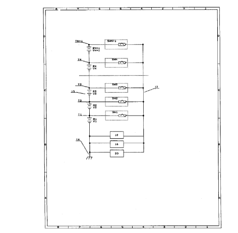
Referring first to Figure 1, a battery assembly 10 is shown
comprising a series of battery modules B1 through B N+l connected in series. It
is to be understood that the terms "battery assembly" and "battery module" are
used throughout the specification to refer to a series of battery cells, or to one or
more interconnected including holders, battery hold, battery receptacles,
housing or clips etc., adapted to house a plurality of individual battery cells in
series. A common sensing wire 12 is shown connected to a series of reference
termin~ T 1 T N+l including end reference terminal N+1 through respective
switching means SW 1 to SW N+l associated with respective battery module B 1
through B N+l. The respective non-linear component switching means SW 1 to
SW N+l are adapted to serially open the switching means between the sensing
wire and successive reference termin~l~ in response to injections of voltage or
current in the form of pulses or continuous outputs, including
voltages/currents of successively increasing magnitude supplied by a
voltage/current generating means 16, for example, a voltage/current step
generator. The common sensing wire is connected to means for detecting a
rapid change in impedance 18 which may be embodied in a variety of forms, as
discussed below. The invention also includes means 20 for instantaneously
measuring voltage and or current in response to a rapid change of impedance
and, combined therewith or separately therefrom, means to provide output
indicating the condition of at least a deteriorating one of said individual
batteries cells based on the instantaneous voltages and/or currents and/or
impedance measured, preferably by displaying the output in human or
9 211 71B6
computer readable form.
The apparatus and method of the invention will now be explained
with reference to Figure 2 showing a preferred embodiment of the invention in
which each non-linear component switching means NLC 1 to NLC N+l
5 comprises a resistor and diode. The respective resistors and diodes are
identified in Figure 2 as RS1 through RSN and DS1 to DSN, respectively. In
operation, when voltage supplied by the capacitor 16 approaches the voltage
equal to V1 the diode DSl will stop conducting and the impedance of common
sensing wire 12 will rapidly change. Voltage and current of the common
10 sensing wire 12 is then measured. The first measured voltage V1 and/or
current of the sensing wire is then stored for further calculation.
Subsequently, through further charging of the capacitor the voltage of the
common sensing wire 12 incrementally rises again and the next sudden
change in the impedance occurs since the diodes DS2 has stopped conducting.
15 The voltage V1 + V2 can be measured at that moment and a simple algorithm
permits V1 and V2 to be calculated. This process is repeated until the last stepof the impedance change is detected. Then the voltage injected into the
common wire is reset again to zero using discharge switch 22 by discharging
the capacitor 16 through resistor 24. Voltage and/or current measurements
20 are made by means adapted for instantaneously measuring voltage and/or
current 20 in response to detection of a rapid change of impedance, preferably
in the form of a microprocessor which preferably combines a means for
evaluating the condition of individual battery cells based on the measured
instantaneous voltage and/or currents and/or impedance and a means to
25 provide output indicating the condition of at least a deteriorating one of said
individual batteries cells.
Any method of detecting a rapid change in impedance can be
employed to carry out the invention. According to one preferred embodiment a
small AC ripple of a much higher frequency than the process repetition is
-10- 2117166
~injected into the slensing wire, from the AC generator 26 either in the form of voltage or current. The response is monitored by measuring the
instantaneous value of the non-injected parameter (voltage when current is
injected or current when voltage is injected). Synchronous detection of that
5 parameter with double *equency allows the detection of any even harmonics of
injected frequency.
These even harmonics will be generated during the transition
period, ie. when the diode is about to stop conducting. Hence, detecting the
presence of even harmonics will define the point at which the voltage of the
10 sensing wire is equal to or at least very close to the battery voltage to which the
diode being turned off is connected.
Another preferred method of detection of the transition period is to
include the impedance of the sensing wire into the resonance circuit of an
oscillator and detecting the change in the free-running oscillation *equency of
15 the circuit attributable to changes in the impedance. In this case a
combination of diode, capacitor and resistor might be used as the non-linear
component switching means. As long as the number of conducting diodes
does not change, the *equency of the circuitry doesn't change either. When
the transition occurs (diode will stop to conduct), the change in the frequency
20 will follow and can be easily detected. Similarly, phase detection of the current
versus voltage in the forced frequency generation can be used.
Another preferred method of detecting a change in impedance is
to determine which diodes are conducting by comparing the plot of the voltage
versus the current of the common sensing wire to the reference plot stored in
25 the microprocessor. By mathematically subtracting those two plots, it is
possible to determine where the sudden change of impedance occurred and to
calculate the voltage at that point. It is understood that the term "plot" or
"plotting" is used throughout the specification to refer broadly to any algorithm
which can be used to model the plotting of graphs to calculate the point of
sudden change of impedance.
It is noteworthy that the voltage drop across the diode is
irrelevant. It simply will shift the measured point up by that voltage drop. It
is important that all diodes used in shown in Figure 2 be identical. The most
5 obvious choice for low voltage systems are Schotky diodes and for higher
voltage systems, ordinary diodes.
Described below with reference to Figures 3 and 4 is yet another
method apparatus for carrying out the invention using field effect transistors,
diodes and capacitor networks in conjunction with the common sensing wire.
Multiple switching means 10 are connected between the sensing
wire 12 the respective battery modules 14 as shown in Figure 3a-3d. It is
understood that switching means as illustrated in Figure 3a - 3d can be identified.
Multiple of any type of the switching means illustrated in Figure 3a, 3b, 3c, and
3d may be used. The switching means 10 each comprises a transistor 16 which is
shown in the preferred embodiments of Figures 3a-3d as an N channel MOSFET.
Each switching means 10, also includes a resister 24 and a diode 26. The diode 26
is connected between the source of the transistor 16 and the end of resistor 24
proximal to the respective battery modules 14. The other end of the resistor 24 is
connected to the gate of the transistor 16.
The terminal T0 of the battery string is shown in common with a
voltage supply means preferably in the form of means of applying a charge pulse
20, and voltage sensing and output means 22. However it is understood that
either component maybe located at any point in the overall circuit as long as it is
connected between the sensing wire 12 and a battery module terminal. It is also
understood that the voltage sensing and output means 22 may comprise separate
sensing and output means. Also, the means of applying the charge pulse 20 is
understood to comprise a means of applying a sink or source current.
In an preferred embodiment of the invention the charge pulse has a
negative polarity and its amplitude is higher than the most negative end of the
-12- 2117166
~attery string. However, if P Mos channel transistors are used, the polarity of all
diodes and battery modules and voltages should be reversed. It is also possible to
use J-FETS as a transistor 16. The following description is true for N-channel
MOSFETS BUT APPLIES MUTATATIS mutandisTO P-channel MOSFETS.
Initially, the potential of the sensing wire 12 is raised up by the
means of applying a charge pulse 20 to a level higher that the total voltage of the
battery string. As a result, all internal diodes of the transistor 16 in each
switching means 10 will conduct and provide a charging path for the internal
capacitor ie. GATE-SOURCE of the transistor 16 via resistor 24. As long as the
charging pulse is maintained, all GATE-SOURCE internal capacitors of all
transistors 16 will remain charged. Polarity of this charge is such, that when the
charge pulse is removed, the remaining charge across the GATE-SOURCE of the
internal capacitors of each transistor 16 will maintain the transistors 16 in the
conducting state. As a result of that the sensing wire potential will be
maintained at the level of the total string voltage as long as voltage between the
gate and source of transistor 16 in the switching means 10 most remote from
terminal T0 is sufficient to keep this transistor 16 in the conducting state.
The fact that the other transistors 16 in all remaining switching
means are conducting is irrelevant because all remain diodes 26 will be polarized
in non-conductive direction.
With the charge pulse absent, the internal GATE-SOURCE capacitor
of the transistor of the switching means N+1 will start to discharge until it
reaches a point when this transistor will stop conducting. Only switching means
N+1 will be open because as long as it is conducting, the internal capacitor of the
GATE-SOURCE of the remaining switching means 10 will be maintained in
charge condition. As soon as switching means N+1 ceases to conduct, the
adjacent switch means N will start to conduct and will present to the sensing
wire 12 a voltage equal to the total battery string voltage less one battery module
(BN+1). The process will repeat itself with each respective switching means 10
-13- 21~716~
subsequently ceasing to conduct at successive intervals.
In a preferred embodiment of the invention an external capacitor 28
may be added to increase the discharge time as shown in Figure 3B.
In a further preferred embodiment of the invention, when the
5 battery string voltage is higher than the permitted voltage across the gate and
source of the transistor 16, a Zener diode 30 can be added to the circuit shown in
Figure 3a or 3b between the gate and source of this transistor for protection
purposes preferrably in the manner shown in Figure 3C.
As shown in Figure 3d, an additional resistor 32 and diode 34 can be
10 added to the circuit shown in Figure 3a [or 3(b), or 3(c) - not shown] across resistor
24 in order to enhance charging time. As shown in Figure 4 the sensing wire
voltage will descend in a staircase pattern with the time of each step determined
by value of total capacitance across GATE SOURCE of each transistor 16 and the
discharge resistor 24. If all switching means 10 are identical the duration of each
15 potential step will be approximately the same. It is possible however to enhance
the duration of the potential steps by changing the product of R1 and the total
capacitance between the GATE-SOURCE of each switching means 10, as given by
the formula T= R X C.
Voltage sensing and output means 22 will preferably respond to each
20 discrete step of the voltage, with individual cell voltages being the difference
between each step, thereby providing accurate measurement of each cell in the
battery string.
DESCRIPTION OF FIGURE 4:
Figure 4 represents a graph of the sensing wire voltages in the
25 circuit when N channel MOSFET transistors are used.
This drawing represents the voltage of the common sensing wire 12
with respect to the battery (any point of the battery string). Y-axis representsvoltage and X-axis represents time.
At the time A a charge pulse is applied of amplitude bigger than the
~ -14- 21~171~
total voltage of the battery Vn. Polarity of this pulse depends of the type of the
transistors used in the switching means and polarity of the battery. Figure 4
shows the case when negative pulse is applied for the duration required to
charge all gate source capacitors of each switching means.
When this pulse is removed at the time B, total voltage of the
sensing wire collapses to a level equal to approximately Vn+l. At that moment,
the gate source capacitor of the switching means 10 connected between Bn and
sensing wire 12 will start to discharge. Some time after, at the moment C, this
capacitor will discharge to such a level that switching means can not conduct
anymore.
As result of this, voltage of the common sensing wire 12 will drop
further to the level D which is the total voltage of all battery cells from Vl to Vn-
1. The difference of the voltages measured at the point C&D represents absolute
value of the voltage of the cell Vn.
The process then repeats itself until point E at which time the
voltage of the sensing wire 12 will reach zero and all gate source capacitors of all
switching means will be discharged.
At point G, the charge pulse is again applied in preparation of the
circuit to repeat the process again.
As many changes can be made to the invention without departing from
the scope of the invention, it is intended that all material contained herein byinterpreted as illustrative of the invention and not in a limiting sense.