Note: Descriptions are shown in the official language in which they were submitted.
''O 94/06267 PC~r/US93/07937
-
-- 1 --
I
HEAT SINK
Field of the Invention
This invention relates to the field of heat sinks
; 5 and in particular to heat sinks for use in small
electronic devices or devices in which there is little
clearance for heat sinks.
Backqround of the Invention
A great deal of effort in the electronics industry
10 today is devoted to trying to produce the electronic
product in the smallest possible package, while at the
same time enhancing the product's performance. Nowhere
is this trend more evident than in the computer field,
where personal computers have become increasingly smaller
15 over the last few years. At the same time, the
manufacturers have also tried to make the smaller
computers as fast and as powerful as possible. This
creates a problem in terms of heat dissipation.
In general, the more powerful the electronic semi-
20 conductor, the more heat it generates. Unless the heatis dissipated, the semiconductor may fail. There are a
variety of well known devices for dissipating such heat.
These include various finned heat sinks, which dissipate
heat through the surface area of metal fins, and which
25 may be and often are in connection with computers used in
conjunction with electric fans, which drive air through
the fins to enhance their cooling effect. Other types of
heat sinks are also used, as well as other cooling
devices such as cooling tubes, which extend around the
30 devices and which carry a flow of some cooling medium.
The problem with these existing devices is that they tend
to take up a good deal of space. In fact, in many
applications, the heat sinks, fans or other cooling
devices take up more space than the semiconductors they
35 are designed to cool. Moreover, these heat sinks and
other related devices tend to take up "vertical" space. That is they tend to have a
significant height, so that it becomes difficult to put them in a thin electronics
package, at least without so severely downsizing them as to make them generally
ineffective. By the same token, the effort to minimize the package for electronic
devices such as portable computers by making them as thin and small as
possible, while not sacrificing speed and power, makes the need for such heat
dissipation means in these packages all the more acute.
Accordingly, an object of the invention is to provide a heat sink,
which provides a significant amount of heat dissipation, while taking up very little
10 space, particularly very little vertical space.
Summary of the Invention
The invention provides a heat sink dissipating heat from one or more
semiconductors on a printed circuit board comprising: a plate having a top
surface and a bottom surface, said plate being made of heat conductive material;
said plate having at least one chimney means, each said chimney means including
a tapered sidewall defining a first opening in said bottom surface of said plate and
a smaller second opening in said top surface of said plate, so as to convect
heated air from the area adjacent to said bottom surface of said plate to the area
adjacent to said top surface; attachment means connecting said bottom surface of
20 said plate to the semiconductors so that said plate conducts heat generated by the
semiconductors when the semiconductors are in operation; and connecting means
connecting said plate to a printed circuit board.
The plate is adapted to fit over an entire circuit board, contacting the
electronic semiconductors on the board, with the chimneys being spaced
71 770-5
' 1~
7. 7 ~
~~ inbetween. The chimneys are designed to facilitate natural or forced airflow
through the plate by reducing the pressure drop associated with such openings.
When in use, the heat sink of this invention takes up very little space, while
providing effective heat dissipation for a variety of electronic components on a
board.
In the preferred embodiment, a heat sink according to the invention
comprises a flat copper plate coated with an electrically insulating, black epoxy
paint. The plate is sized in relation to the board on which it will be used, but six
inches by 9 inches would be a common size. The plate is 20 thousandths inches
10 thick. The heat sink includes a series of holes interspaced over its surface. The
location of the holes depends upon the
- 2a -
71 770-5
CA ~ l 1 7~7 1
~094/06267 PCT/US93/07937
~.
-
-- 3
configuration of the electronic elements on the board towhich the heat sink is intended to be applied. In
general, however, the holes are disposed so as to be
located above the pathways between the electronic devices
5 on the board, once the heat sink is in place. The holes
are not cylindrical. Instead, they have a wide bottom
and curved, tapering sides extending upwardly to a
narrower open top disposed about a tenth of an inch above
the rest of the plate of the heat sink. The heat sink of
10 the preferred embodiment also includes alignment holes to
assure proper placement of the heat sink on the board
over the electronic devices. Proper placement is also
aided by a series of indents on the underside of the heat
sink, which indents serve to help properly align the heat
15 sink with the electronic devices over which the heat sink
is to be placed. The heat sink is held to the board by
connectors at its corners, and double-faced, heat
conductive tape attaches the semiconductive devices on
the board to the underside of the heat sink of this
20 invention. In operation, the heat sink dissipates heat
from all the electronic devices on the board to which the
heat sink is attached, and the holes or chimneys provide
airflow passages with low pressure drops to facilitate
cooling airflow around the electronic devices to further
25 dissipate the heat they generate. At the same time, the
heat sink of this invention takes up very little vertical
space on the board.
DescriPtion of the Preferred Embodiment
I turn now to a complete description of the preferred
30 embodiment, after first briefly describing the drawings.
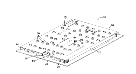
Figure 1 is a perspective view of a heat sink according
to this invention mounted on a printed circuit board;
Figure 2 is a top view of the heat sink of Figure 1;
Figure 3 is an expanded view of a portion of the side of
35 the heat sink of Figure 1;
CA21 1 7271
W094/06267 PCT~US93/079
Figure 4 is an expanded view of one of the
chimneys of the heat sink of Figure l; and
Figure 5 is an expanded view of an edge of the
heat sink of Figure 1.
5 Structure
Referring to Figure 1, a heat sink according to
the invention is shown at 10. The heat sink 10 generally
comprises a plate 20 having a top surface 22 and a bottom
surface 24, with a series of chimneys 30 extending
10 therethrough. The heat sink 10 is shown in Figure 1
attached to a printed circuit board 40, upon which is
mounted a number of semiconductor devices 50 (only
partially shown in Figure 1).
Referring to Figures 1 and 2, the plate 20 is
15 rectangular and has approximately the same length and
width as the printed circuit board 40. In the preferred
embodiment, these dimensions are six inches by nine
inches. Other sizes and shapes are possible without
departing from the invention herein, and it is not always
20 necessary for the heat sink 10 to cover the entire
printed circuit board 40. The plate 20 is made of copper
in the preferred embodiment and is about .020 inches
thick. Other materials may, of course, be used. For
example, aluminum may be used for applications where the
25 heat needed to be dissipated is not as great, or where a
lighter materi~l is needed. Other metals may also be
used. The plate 10 is coated with a black epoxy paint
which provides electrical but not thermal insulation.
Such a paint is CC3-341 from Cast Coat, Inc. of West
30 Bridgewater, Massachusetts. The paint covers the entire
plate 10 including both the top surface 22 and the bottom
surface 24.
As shown in Figures 3 and 4, all the chimneys 30
on the plate 10 are identical and generally coni¢al in
35 cross section. Each such chimney 30 has a bottom opening
~21 1 7~71
YO94/06267 PClVUS93/07937
,_
_
32 disposed on the bottom surface 24 of the plate.~ In
the preferred embodiment, the diameter of the bottom
opening is .400 inches for each chimney, although other
dimensions are possible. As best shown in Figure 4, each
s chimney 30 has an inwardly curved sidewall 34 which
extends from the bottom opening 32 to a top opening 36.
The top opening has a diameter of .200 inches in the
preferred embodiment, and the sidewall 34 extends .100
inches above the top surface 22. Other dimensions are
10 possible here. With these dimensions, however, the
chimney 30 has an internal area several times greater
than that of a hole with a .200 inch diameter through the
plate 20. In the preferred embodiment, the chimneys 30
are created by a conventional extrusion process.
As best shown in Figure 2, the placement of the
chimneys 30 is not random. In Figure 2, there is shown
in dotted display beneath the plate 20, the location of
the semiconductor devices 50 to be cooled by the heat
sink 10. Also shown in dotted display is the location of
20 other electronic components 60 mounted on the particular
printed circuit board 40 shown in the Figures. This
configuration of semiconductors ~0 and other electronic
components 60 depends upon the printed circuit board 40
with which the heat sink 10 is to be used. The
25 arrangement shown here is for illustrative purposes only.
As is typical of many printed circuit boards, the
semiconductors 50 and other electronic components 60 are
arranged more or less in rows so that open, air-flow
passageways 62 exist between components. In general, as
30 shown in Figure 2, the chimneys 30 are disposed in the
plate 20 above the intersection of such passageways 62 on
the board 40 and above otherwise open areas on the board
40.
As also shown in Figure 2, the plate 20 has a
35 series of location holes 26 therethrough. The location
~ ~ ~'J ~ ~ ~
holes 26 are disposed over opposite corners of the semiconductors 50 when the
heat sink 10 is properly aligned over the board 40. The holes 26 allow a visual
means by which this alignment can be determined. The location of the hole 26
depends, of course, on the location of the semiconductors 50 on the particular
board 40 and thus may vary from board to board. In addition, for key
semiconductors, such as microprocessors, a triangular inspection hole 28 is
provided so that a visual inspection of pin number one of the microprocessor may
be made when the heat sink 10 is in place so that it can be determined whether or
not pin one on the device is properly positioned.
As shown in Figure 3, another alignment means is provided in the
form of ridges 29 which extend from the bottom surface 24 of the plate 20. The
ridges, which are about .030 inches high in the preferred embodiment, are
disposed to be adjacent to each semiconductor 50. As a result, when the heat
sink 10 is put in place, the ridges 29 provide a guide for correct positioning over
the semiconductors 50.
As shown in Figures 1 and 5, the heat sink 10 has a pair of sides
12, 14. The sides 12, 14 extend down the lengthwise sides of the plate 20. As
shown in Figure 5, the sides 12, 14 are formed by folding over the edges of the
plate 20, although other means could be used. Connectors 16 are attached to the
sides 12, 14 at their ends, and the connectors 16 are used to attach the heat sink
10 to the printed circuit board 40. Any standard type of connector may be used.
71770-5
CA~l 1 727~
"O 94/06267 PC~r~US93/07937
It is also possible to have the sides 12, 14
extend completely around the plate 20 so as to partially
close off the ends. While this restricts airflow
somewhat, it is useful in situations where the board
5 needs to be shielded from electro-magnetic radiation
(EMR) or radio frequency interference (RFI).
Operation
In operation, the heat sink 10 is made so that the
chimneys 30, inspection holes 26, 28 and ridges 29
10 correspond, as indicated previously, to the configuration
of the printed circuit board 40 on which the heat sink 10
is to be used. The semiconductors 50, which are to be
attached directly to the heat sink 10, each have a piece
of double-sided, heat conductive tape 52 placed on its
15 exposed upper surface. The heat sink 10 is then lined up
with the semiconductors 50 using the ridges 29 and
inspection holes 26, 28. When properly aligned, the
connectors 16 are attached to the board 40 by inserting
them into holes (not shown) in the board, and the heat
20 sink 10 is then attached to the board 40. The tape 52
thermally connects the semiconductors 50 to the bottom
surface 24 of the plate 20 of the heat sink 10. In
operation, heat from the semiconductors 50 is dissipated
by the heat sink, which has a significant amount of
25 surface area compared to the semiconductors 50. In
addition, to aid in the cooling, the configuration of the
chimneys 30 creates a low pressure drop between the air
adjacent to the bottom surface 24 and the top surface 22
of the plate 20. As a result, air flows easily up
30 through the chimneys 30 from the underside of the plate
10 to the upper side, by means of natural convection,
without the need for forced air blowing. Of course,
forced air blowing may be used with the heat sink 10 of
this invention, and applied at one of the open ends not
35 covered by a side 12, 14.
CA21 1 7271
W094/06267 PCT/US93/079
Other embodiments will occur to those skilled in
the art. What I claim is: