Note: Descriptions are shown in the official language in which they were submitted.
CA2ii7426
WO 93/15524 PCT/US93/00992
FERMI THRESHOLD FIELD EFFECT TRANSISTOR
WITH REDUCED GATE AND DIFFUSION CAPACITANCE
Field of the Invention
This invention relates to Field Effect
Transistor devices and more particularly to high speed
Field Effect Transistors having reduced gate and
diffusion capacitance.
Back4round of the Invention
Field Effect Transistors (FET) have become
the dominant active device for very large scale
integration (VLSI) and ultra large scale integration
(ULSI) applications, because the integrated circuit FET
is by nature a high impedance, high density, low power
device. Much research and development activity has
focused on improving speed and density of FET's, and on
lowering the power consumption thereof. U.S. Patents
4,984,043 and 4,990,974, both to the present inventor
Albert W. Vinal, and both entitled Ferm~. Threshold
Field Effect Transistor, describe a high speed, metal
oxide semiconductor (MOS) FET which has a threshold
voltage which is independent of insulator thickness,
channel length, drain voltage, substrate doping and
temperature to provide a high speed FET. However,
notwithstanding the vast improvement of the Fermi
threshold FET compared to known MbS devices, there is a
CA 02117426 1999-OS-OS
-2-
continuing need to lower the capacitance of the Fermi
FET structure.
German Offenlegungsschrift DE 31 38 747
describes a depletion-mode field-effect transistor
having a depletion region (10) between the source
region (2) and drain region (3) which has the same
conductivity type as the latter, and additional
semiconductor regions (11 and 12) between the source
region (2) and the drain regioh (3), which have the
same conductivity type as the~latter and which form a
common, flat p-n junction (13) with the substrate.
Summary of the Invention
It is therefore an object of an aspect of the
invention to provide an improved Fermi threshold Field
Effect Transistor (FET).
It is another object of an aspect of the
invention to provide a Fermi threshold FET with reduced
gate and diffusion capacitance.
These and other objects of aspects of the
invention are provided, according to the present
invention, by providing a Fermi-FET structure which
allows conduction carriers to flow within the channel at
a predetermined depth in the substrate below the gate,
without requiring an inversion layer to be created at the
surface of the semiconductor in order to support carrier
conduction. Accordingly, the average depth of the
channel charge requires inclusion of the dielectric
constant of the substrate to calculate gate capacity.
Gate capacity is thereby reduced.
The low capacity Fermi FET is preferably
implemented using a Fermi Tub region having
predetermined depth, and with a conductivity type
opposite the. substrate conductivity type and the same
conductivity type as the drain and source diffusions.
The Fermi Tub extends downward from the substrate
suesm'uTE s~~'
CA 02117426 1999-OS-OS
-3-
primarily determined by the depth of the Fenai channel
and the carrier distribution in the channel and is
relatively independent of the thickness of the gate
oxide layer. The diffusion capacity is inversely
dependant on the difference between the sum of the
depth of the Fermi Tub and the depletion depth Y, in the
substrate and the depth of the diffusions. A low
capacity Fermi FET is thsreby provided.
In accordance with one embodiment of the
invention, a field effect transistor comprises a
semiconductor substrate of first conductivity type,
having a first surface;
a tub region of second conductivity type in the
substrate at the first surface;
spaced apart source and drain regions of the
second conductivity type in the tub region at the first
surf ace ;
a gate insulating layer on the substrate at the
first surface, between the spaced apart source and drain
regions; and
source, drain and gate contacts for
electrically contacting the source and drain regions and
the gate insulating layer, respectively;
characterized in that the field effect
transistor further comprises a channel of the second
conductivity type in the tub region at the first surface,
between the spaced apart source and drain regions;
wherein the channel extends a first predetermined depth
from the first surface, wherein the tub region extends a
second predetermined depth from the channel, wherein the
source region extends a third predetermined depth from
the first surface, and wherein the third predetermined
depth is greater than the first predetermined depth and
less than the sum of the first and second predetermined
depths.
CA 02117426 1999-09-16
3a
Figure 1 graphically illustrates substrate
doping as a function of channel length to maintain
breakdown voltage o! 8 volts.
Figure 2 graphically illustrates depletion
area capacity at zero drain voltage as a function of
channel length that corresponds to the doping
concentration shown in Figure 1.
Figure 3 is a cross-sectional view of a known
buried n-channel MOSFBT.
Figure 4 is a cross-sectional view of a Fermi
FET.
Figure 5 is a cross-sectional view of the
Fast Fermi F8T according to the present invention.
Figures 6-10 are cross-sectional views of
channel conduction in the Fast Permi FBT of Figure 5
with increasing Bata voltage.
Figure 11 graphically illustrates a profile
of excess carrier injection as a function of Fermi
channel depth.
Figures 12a and 12b are drain currant plots
for P-channel MOSFETs and Fast Farmi FET devices of
identical size.
Figures 13a and 13b graphically illustrate
gate capacity for a P-channel Fast Fern FET and a P-
channel MOSFET, respectively.
Figure 14 is a plot of the ratio of MOS to
Fsrmi gate capacity as a function of oxide thickness.
CA 2 i i 1426
WO 93/15524 PCT/US93/00992
Figure 15 depicts the electric field diagram
for an N-channel Fast Fermi FET.
Figure 16 graphically illustrates Fermi
channel depth as a function of poly dopant
concentration.
Figure 17 graphically illustrate Fermi Tub
depth versus poly dopant concentration.
Figure 18 graphically illustrates threshold
voltage versus poly dopant concentration.
Figure 19 illustrates delta flatband voltage
versus poly dopant concentration.
Figure 20 is a cross-sectional view of the
depletion region surrounding the diffusions that are
provided by the Fermi Tub.
Figures 21a-21d illustrate measured substrate
body effect and measured source body effect for
conventional MOSFETs and for the Fermi FET transistor.
Figure 22 illustrates the electrical field
diagram for a conventional MOS device.
Figures 23 and 24 graphically illustrate
threshold voltage versus substrate voltage.
Description of a Preferred Embodiment
The present invention now will be described
more fully hereinafter with reference to the
accompanying drawings, in which a preferred embodiment
of the invention is shown. This invention may,
however, be embodied in many different forms and should
not be construed as limited to the embodiment set forth
herein: rather, this embodiment is provided so that
this disclosure will be thorough and complete, and will
fully convey the scope of the invention to those '
skilled in the art. Like numbers refer to like
elements throughout.
An improved Fermi FET structure is disclosed
where gate and diffusion capacitylare substantially
lower than corresponding values attainable from MOS
C~2~i742~
WO 93/15524 PCT/US93/00992
-5-
FET's and prior art Fermi FET device designs. A new
Fermi FET structure is described that allows conduction
carriers to flow within a channel of predetermined
depth in the substrate below the gate. This new
structure was conceived as a result of theory and
experimentation with conventional Fermi FET and MOS FET
structures. The Fermi FET structures are described in
patent Nos. 4,990,974 and 4,984,043 the disclosures of
which are incorporated herein by reference. It was
discovered that certain electrical and physical
conditions must be observed in order for carrier
conduction to flow within a channel region at
substantial depth in the substrate below the gate oxide
layer. In contrast, conventional MOSFET devices
require an inversion layer to be created at the surface
of the semiconductor in order to support carrier
conduction. The depth of the inversion layer is
typically 200 Angstroms or less. Under these
circumstances gate capacity is essentially the
permittivity of the gate insulator layer divided by
it's depth. In other words, the channel charge is so
close to the surface that effects of the dielectric
properties of the substrate are insignificant in
affecting gate capacity. Gate capacity can only be
lowered if conduction carriers are confined within a
channel region below the gate where the average depth
of the channel charge requires inclusion of the
dielectric constant of the substrate to calculate gate
capacity. In general Fast Fermi FET gate capacity is
described by the following equation.
C = 1
1'f Tox ~ l 1 )
ei
CA2ii7426
WO 93/15524 PCT/US93/00992
-6-
Factor Yf is the depth of the conduction channel called
the Fermi Channel, e, is the permittivity of the
substrate, Q is the factor that determines the average
H
depth of the charge flowing within the Fermi Channel
below the surface. R depends on the depth dependant
profile of carriers injected from the source into the
channel. For the Fast Fermi FET, ~~2. Tax is the
thickness of the gate oxide layer and ei is its
permittivity.
According to (1), gate capacity may be
reduced by a factor of 2 by simply controlling the
depth Yf of the Fermi channel and the source injection
profile defined by Q. Specifically, a Fast Fermi gate
capacity is 1/2 the MOS value ei/Tox when:
Yf = Tox ( Z )
~ e9 e~
For this condition, the Fermi channel depth Yf
must be greater than;
~,fZ ~-'sTox~ ( ~ )
ei
Typically, Yf > 6Tox for p=2
The conditions that allow conduction carriers
to flow at substantial distances below the surface of
the semiconductor are not obvious. Considerable theory
supported by experimentation were required to discover
the requirements. There are two primary conditions ,
that must be observed.
1. When excess carrier~conduction occurs, no
perpendicular electric field component should exist in
CA2ii742~
WO 93/15524 PCT/US93/00992
the channel region other than that produced by the
excess carriers themselves.
2. The injection barrier potential KT/q
Ln (NdN~/N12) must be reduced to zero at the bottom of the
Fermi channel before the barrier is lowered at the
top.
3. The dopant density within the source
diffusion, as a function of depth, must decrease at a
prescribed rate in order to support the proper depth
profile for gate induced carrier injection into the
channel.
Dynamic gate capacity can only be measured
using actual transistor structures with drain voltage
greater than zero. Gate area is defined by the area
between the source and drain. The usual technique of
measuring MOS gate capacity fails to reveal real
dynamic gate capacity in Fast Fermi FET devices due to
parasitic stray charge and the lack of an injection
profile. Gate capacity measured from real transistors
is a means of monitoring product and is used as a
process control measurement.
The speed of digital circuits depends
directly on diffusion depletion capacity. Low
diffusion depletion capacity is inconsistent with short
channel MOSFET devices. Depletion capacity is
essentially the ratio of the substrate permittivity and
the total depletion depth surrounding the drain or
source diffusion. There are two components of
diffusion depletion capacity, area and perimeter. Area
capacitance occurs at the bottom of the diffusion.
Perimeter capacitance is known as sidewall capacitance.
Sidewall capacitance can dominate the area capacitance
in MOS devices because of the increased substrate
~ dopant adjacent the diffusions to provide channel stop
regions. The Fast Fermi FET avoids the need for
channel stops.
Sidewall capacity is defined below;
CA2ii7426
WO 93/15514 PCT/US93/00992
-8 _ w-
C'dp=Csw ~ 2 Ld+Zl Xd
Area capacity is defined as
Cda=CaLaZ (4b)
where;
Z = Channel width
Xd = Depth of the diffusion
Ld = Length of diffusion
For the Fast Fermi FET device;
eg
Caw Yo+YP
C.= ee
a t Ycub-Xa) +Yp
Where;
e, is the permittivity of the
semiconductor material and Yn+YP is the total depletion
depth surrounding the drain or source diffusion, Y?"b is
the depth of the Fermi Tub. Yo + YP is the side wall
depletion depth and Xd is diffusion depth.
MOS depletion depth is inversely dependant
on substrate doping concentration N,. In MOS devices
for example a fundamental voltage breakdown condition
exists called Punch-through. The substrate dopant
concentration required for MOSFET's to prevent °
punch-through is given below as a function of channel
length and breakdown voltage.
CA2ii7426
WO 93/15524 PCT/US93/00992
_9_
2
2e$Vo a Va (5)
N = 1+ 1+-.
q 1+a Vo
V = KT 1 NaNs
q ~ Ni
Na
a=
Ns
Diffusion capacity has the following
expression
= qNsesa ~6)
a 2 ( Vo+Va) ( a +1 )
Figure 1 is a plot of substrate doping as a
function of channel length to maintain a breakdown
voltage of 8 Volts.
Figure 2 is a plot of Depletion area capacity
(F/cm2), at zero drain voltage, as a function of channel
length that corresponds to the doping concentration
shown in Figure 1
It is apparent that substrate doping
requirements increase rapidly as channel length is
shortened to cope with the punch-through mechanism.
For short channel MOS devices (0.8u) or less a
diffusion capacity of 0.5x10-' F/cm2 or greater is
typical. This value of diffusion capacity is reduced
by a factor of about 3 by the new Fast Fermi FET
device. Punch-through is eliminated by the unique
Fermi Tub method used to construct the Fast Fermi FET.
Punch-through is eliminated while being tolerant of
variations in diffusion depth. Fqr short channel Fast
Fermi FET devices, a substrate dopant concentration of
1E16 is typical.
CA2ii7426
WO 93/15524 PCT/US93/00992
-10-
The new Fast Fermi FET design simultaneously
solves several fundamental problems characteristic of
short channel FET devices, while providing the solution
to attain low gate capacity.
1. Eliminates punch-through.
2. Virtually eliminates threshold voltage
dependance on oxide thickness.
3. Dramatically lowers area and sidewall
depletion capacity.
l0 4. The Fermi Tub design greatly simplifies
fabrication of P-channel devices.
5. Enhances saturation current for a given
gate voltage despite the reduction of channel charge
per unit gate voltage.
6. P and N channel devices use the same
design criteria.
7. Maintenance of 5 volt power sources.
8. Eliminates drain induced barrier lowering
commonly experienced by buried channel devices.
9. Eliminates threshold voltage off-set due
to a difference in the flat-band voltage between the
poly gate and substrate contacts.
10. Greatly suppresses hot electron
problems.
11. Eliminates the need for channel stops.
12. Allows unique control of threshold
voltage.
13. Provides for extremely low body effect.
Discussion
The operating speed of digital integrated
circuits depends on 6 basic transistor parameters in
addition to parasitic capacitance effects associated
with interconnecting circuits. Logic circuit delay
time ultimately controls the speed of integrated
circuits. It can be shown that delay time in a chain
of logic cells can be compiled into a single equation.
CA2ii742b
WO 93/15524 ~ PCT/US93/00992
-11-
2
Ta=~VaaLo (1+~) aCd Lo +(3 C9+Y Cc Lo o(Wc~) ~ (7l
sa tn
There are six basic transistor parameters that govern
logic delay time and ultimately system speed.
1. Square channel saturation current I*"in~
This term defines drain current that flows in an
N-channel transistor whose width is equal to it's
channel length with maximum gate voltage applied.
2. Channel length Lo; the effective length of
the conductive channel
3. Diffusion depletion capacity Cd*,
Farads/cm2
4. Gate capacity Cg*, Farads/cm2
5. Length of the diffusion Ld
6. Ratio n of an N-channel saturation
current to P- channel saturation current.
Referring to Equation 7, it is clear that the
coefficient for delay time depends on the square of
channel length Lo. The coefficient also shows an
inverse dependance on square channel saturation current
of the N-channel device for C-MOS circuit
configurations. Factor ETA, n, is also a part of the
coefficient. This factor defines the ratio of
N-channel to P-channel saturation currents. Parameter
of Equation 7 is derived in patent # 5,030,853 (Ring
Segment Buffer) the disclosure of which is hereby
incorporated herein by reference. There are three
capacitive terms within the bracket term, Diffusion
capacitance Cd*, Gate capacitance Cg*, and interconnect
capacity C~*. Coefficients a, p, and Y account for the
various logic functions within the logic chain that
account for Fan-in and Fan-out fob example.
There are several means available to reduce
time delay in the logic chain. The usual approach is
CA2iil42b
WO 93/15524 PCT/US93/00992
-12-
to reduce channel length, or attempt to increase drain
saturation current. Scaling down transistor size to
achieve shorter channel length devices unfortunately
has a dramatic effect on increasing gate and depletion
capacitance. See Figure 2. Depletion capacity
increases as a result of increasing substrate dopant
density to prevent Punch-through in short channel
devices. Gate capacity increases as a result of
scaling down the thickness of the gate oxide layer Tox.
The gallium arsenide technology for example,
attempts to decrease delay by increasing drive current
capability. Unfortunately GaAs channel mobility, at
the source end of the channel, approaches the silicon
value as channel length becomes less than 0.8 microns.
The tremendous DC power increase due to N-channel
technology compared to C-MOS to attain speed appears to
be impractical in view of FAST silicon devices.
A second and more practical approach to
increasing speed of integrated circuit technology is to
minimize .the load capacity terms Cd*, C8*, and C~*. All
capacitive terms are Farads/cm2. If these capacitive
terms were all zero, circuit delay time would be zero
independent of channel length Lo or saturation current
I*sazn~ The key to lowering diffusion capacity is to
clearly understand and eliminate the punch-through
mechanism. The Fast Fermi FET design eliminates the
punch-through phenomenon and Drain Induced Barrier
Lowering by use of a Fermi Tub technique that surrounds
the diffusions and defines the Fermi channel region.
This unique device geometry reduces gate and diffusion
capacity by as much as a factor of 2.5 or more. The
details of how the Fast Fermi FET lowers gate and
diffusion capacity is discussed in the Fast Fermi FET
Design Section.
Conductor or interconnect capacity C~* can be
i
lowered by increasing field oxide thickness. For a
majority of digital circuit technology, interconnect
CA2ii7426
WO 93/15524 PCT/US93/00992
-13-
capacity can be handled so as to represent about 10% of
the total load capacity. In ot~~er words, if gate and
diffusion capacity were eliminated altogether, system
speed could be increased by a factor of 10 or more.
The key to high speed digital systems is to
' maximize voltage Slew Rate, the ratio of square channel
current and load capacitance while minimizing power.
Minimizing capacitive load (gate and depletion
primarily) while maintaining or increasing drive
to current, is the only way to achieve high operating
speed with the least power consumption. The concept of
reducing gate capacity while maintaining the same drive
current is intimately involved with the effect mobile
carrier density in the channel has on individual
mobility of carriers in the channel. Since FET drain
current involves the product of gate voltage and gate
capacity, or charge, the Fast Fermi FET technology
achieves the same or better current capability with
substantially less total charge flowing in the channel
per unit current.
Fast Fermi FET Design
There is a fundamental addition to the basic
Fermi FET structure disclosed in the referenced
patents. This addition reduces gate and depletion
capacity according to the present invention. This
basic change can be seen by comparing the new
structure, Figure 5 with the prior art structures of
Figure 3 and Figure 4.
Figure 3 illustrates a basic prior art buried
P-channel MOS device. There are two fundamental
problems with this prior art structure. First, voltage
breakdown occurs due to the punch-through mechanism.
Second, the phenomenon of drain induced barrier
lowering occurs that tends to turn the channel "ON"
when drain voltage is applied. Both problems are a
result of diffusion-gate induced charge sharing in the
CA2ii7426
WO 93/15524 PCT/US93/00992
-14-
substrate depletion region below the buried channel.
This buried channel structure like MOS devices requires
a heavily doped substrate region to minimize these
effects. The result however is to dramatically
increase diffusion capacity. The motivation for the
shallow buried channel device apparently was an attempt
to enhance saturation current for a given gate voltage.
Figure 4 illustrates the prior art Fermi FET
structure. This device design avoids drain induced
to barrier lowering and punch-through when the depth of
the channel Yo equals the depth of the drain and source
diffusions. For this configuration, substrate doping
need not be high and consequently drain diffusion
capacity can be lowered. However, gate capacity for
this structure is only slightly less than a MOS device
despite the depth of the Fermi channel.
The conditions required to control the
distribution of charge in the channel region during
conduction were unknown when the first Fermi FET device
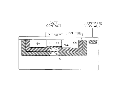
was patented. The structure of Figure 5 depicts the
basic Fast Fermi FET structure of the present
invention. The basic physical difference is inclusion
of a Fermi Tub region labeled in the figure. The Fermi
Tub has the same conductivity type as the drain and
source diffusions and has depth equal to the sum of two
factors, the Fermi channel depth Yf, and depletion depth
Yo. These depth's have specific design criteria and are
discussed subsequently. With this new design, the
Fermi channel Yf is capable of supporting carrier flow
with a unique concentration profile throughout it's
depth. This carrier concentration profile can only be
achieved by the structure design of Figure 5. This
structure also satisfies all of the critical design
criteria required to achieve lower gate capacity.
Referring to Figure 5, the depth c~f the diffusions Xd
must be greater than or equal to the depth of the~Fermi
channel Yf but not to exceed the sum Yf+Yo. Substrate
Cp 2 i i 7426
WO 93/15524 PCT/US93/00992
'""' -15-
depletion depth is labeled Yp in Figure 5. The Fermi
channel Yf is empty of conduction carriers for gate
voltage less than threshold voltage. For this
circumstances gate capacity is quite low and has the
value;
C.= 1
C Yf+Yo+Yp) + Tox L 8 )
eg e1
Diffusion capacity per unit area is also low having the
value
~ es
Cd - C Ytub_Xa) + Yp+ Yn '9'
Channel Conduction Versus Gate Volta4e
Figure 6 through 10 depict the process of
stimulating channel conduction with increasing gate
voltage. All figures illustrate N-channel behavior.
P-channel devices are constructed in identical fashion
by changing all N conductivity type material to P type
and all P type to N type. Figure 6 illustrates the
Fermi Channel completely empty of majority type
carriers. Figures 7 through 9 illustrate ionized
donors in the channel being neutralized from the bottom
up allowing channel conduction to initially commence at
the bottom of the Fermi channel. Excess carriers are
injected from the source for larger gate voltage and
have a unique distribution as shown in Figure 10.
Source to Fermi Channel Injection Profile
Carriers that flow in the channel region of
any FET are injected into the channel region from the
C~2ii7426
WO 93/15524 PCT/US93/00992
-16- ~'
source when gate voltage is applied. Excess carrier
distribution within the depth profile of the channel is
prescribed by the injection mechanism. Majority
carrier injection (or absorption) is a result of the
electric field between the gate electrode and the
surface of the source diffusion facing the channel.
Carriers injected into the end of the channel from the
source must not be restricted to the surface region of
the channel. Instead, injection should be uniformly
to distributed in the depth direction of the Fermi
channel. It is important that the doping profile of
the source diffusion not be uniform but rather the
impurity concentration should be about 2E19 at the
surface and decay with depth by at least 1.0 decade
between the top of the Fermi channel and its bottom.
This gradient is required to achieve a useful
distribution of excess carrier injection throughout the
depth of the Fermi channel thus allowing significant
lowering of gate capacity. Ideally it is desired that
the center of mass of the excess carrier charge lie at
half the depth of the Fermi channel. When the charge
center lies at half the depth of the Fermi channel,
Fast Fermi FET gate capacity becomes:
1
_~
Yf + Tox
2 e$ ei
A typical profile of excess carrier injection
as a function of Fermi channel depth is illustrated by
Figure 11 below.
Dopant concentration at the top of the
diffusion is 2E19 and 5E17at the bottom of the channel.
Notice the unique cusp type of profile. The average
charge position for this cusp distribution is at
approximately half the depth of the Fermi Channel.
CAS ~ ~ ~~~
WO 93/15524 PCT/US93/00992
_17_
Drain Current
Considerable theoretical and experimental
work has been done to prove that drain current is not
sacrificed from the MOS value by the Fast Fermi device
despite substantial reduction of channel charge per
unit of current. The reason is, mobility of conduction
carriers increases in proportion to total charge
reduction. In other words, carrier concentration is
reduced with a corresponding increase in carrier
mobility. Fast Fermi FET channel energy 1/2 CgVg2 is
reduced in proportion to the reduction of gate capacity
along with switching power 1/2 CgVg2f at frequency f.
Figures 12a and Figure 12b are drain current
plots for P-channel MOSFET and Fast Fermi FET devices
of identical size, IrZ=0.8~. and identical oxide
thickness, 165A. The substrate doping for the MOS FET
is 1E17 per cm3 and 1E16 for the Fast Fermi device.
Notice that the Fast Fermi FET conducts more current
than the MOS device for a given gate and drain voltage
despite the fact that gate and depletion capacity are
47% and 30% of the MOS values respectively. The net
result is that the toggle rate of logic circuits
constructed with Fast Fermi FET devices is about 2.5
times the same circuits implemented with MOS FET's for
the same operating power.
Gate Capacity Measurement
There is a vast amount of information in the
literature about MOS capacitance measurements. No
information has been found describing gate capacity
measurements using actual transistor structures.
Perhaps the reasoning has been that the channel charge
is so close to the surface, within a region about 200
angstroms or less, that MOS capacitors tell the story.
This line of reasoning is invalid~for Fast Fermi FET
devices since the injection profile is adjusted for
deep injection depths. The MOS capacitor technique
CA2ii7426
WO 93/15524 PCT/US93/00992
_ 18 _ ..,_
will not reveal gate capacity of the Fast Fermi FET
device. In MOS devices, injection into the ionized
region below the inversion layer is insignificant
because of the barrier height between the source
diffusion and the ionized region facing the diffusion.
Injection however does occur closer to the surface
where the barrier is lowered by the inversion process.
Gate capacity measurements for the Fast Fermi
FET are made using actual transistor structures. A
l0 differential capacity measurement must be made to
remove capacity introduced by contact pads. This
technique is simple and is used to monitor the
manufacturing process. Gate area is well defined as
the product of channel width Z~ and channel length L~.
Transistor structures are required for capacity
measurements since the source injection profile
primarily determines the charge distribution in the
channel and therefore gate capacity. This injection
profile of carriers as a function of depth at the
source end of the channel remains essentially unaltered
in the interval between the source and drain during
transit time. The reason is, there is no vertical
field component across the Fermi channel other than
that produced by the carriers themselves. The vertical
field component resulting from Fermi Tub depletion
across the substrate-Tub junction is zero at the bottom
edge of the Fermi channel and remains zero throughout
the depth of the channel when the Fermi channel is
charge neutral.
Figure 13 a is a plot of gate capacity for a
P-channel Fast Fermi FET and Figure 13b is a similar
plot for a P-channel MOS device.
Referring to Figure 13a for gate voltage with
magnitude below threshold, charge inversion occurs in
the Fermi Channel region. In this region of the plot
gate capacity is
C~ 2 i i 7426
WO 93/15524 PCT/US93/00992
",~ -19-
C.= 1
b + ~'ox ( 11 )
2eg ej
where 6 is inversion depth.
For gate voltage near threshold, gate
capacity is quite low:
C.= 1
9 yo+ yp+ y f Tox ( 12 )
ee ei
For gate voltage above threshold, gate capacity
approaches;
C' = 1
yf Tox (13)
et
Value p depends on concentration gradient
within the source diffusion in the depth direction.
Typically, Q has the value 2Ø
Figure 13b is a plot of dynamic gate
capacitance measured for a MOS transistor. There is
virtually no difference between inversion and
accumulation capacity. The depth of the ionization
region below the gate in the substrate determines the
minimum capacity value for the MOS structure. However
when inversion occurs, capacity abruptly rises to the
conventional value ei/Tox (Area).
In all capacitive measurements that use real
transistors, drain voltage is applied to ensure removal
of parasitic charge and to transport injected charge.
CA2ii7426
WO 93/15524 PCT/US93/00992
-20-
Figure 14 is a plot of the ratio of MOS to
Fermi gate capacity as a function of oxide thickness
given a Fermi channel depth of 1200 angstroms. _
Fast Fermi FET Analysis
The conditions for channel and Tub implant
that will correct for flat-band voltage difference
between the poly gate and the substrate contact will
now be described. Gate and diffusion capacity are
decreased by controlling the depth and dose of the
Fermi Tub region. Figure 15 depicts the electric field
diagram for an N-channel Fast Fermi FET that describes
the mutual depletion of the Tub, channel and substrate
below the gate at threshold conditions.
The electric field component in Figure 15
that rises above the abscissa accounts for the Fermi
channel depth Yf that is included in the Tub implant
depth to minimize the effects of the difference between
the poly gate contact and substrate contact. This
channel depth defines the region that carrier
conduction occurs. This Fermi channel region has
substantial depth and therefore the center of mass of
the conduction charge lies at a substantial depth below
the surface given the correct diffusion-channel
injection profile. These factors account for a
substantial reduction in gate capacity. The threshold
voltage of a prior art Fermi FET is twice the Fermi
potential if the difference between the poly gate and
substrate contact potential is Zero. However in
practice, the dopant concentration in the poly gate
needs to be high in order to eliminate rectifying
contact problems. Therefore the differential flat-band
voltage due to these contact potentials is~
~Q2ii7426
pGT/US93/00992
WO 93/15524
-21-
Of = q 1~~~ (14)
b IN
Where;
Np = Dopant concentration in poly gate.
N, = Dopant concentration in substrate.
This delta flat-band voltage is typically 200
millivolts. Referring to Figure 15, the potential
within the triangle region above the abscissa is:
~= acqNe Yf ( 15 )
2 es
Setting this potential ø to equal delta
flat-band voltage ~fb yields a definition for the depth
of the Fermi channel.
_ 2e90fb (16)
Yf a qNH
Where:
a = N~/N,
N~ = Concentration of contra doping in
Fermi Tub.
N, = Substrate dopant concentration per
cm3
The total depth of the Fermi Tub below the
gate is:
YTub = Yf + Yo % where Yo is the depletion depth in the Tub
due to its contact with the substrate.
2 eg~e ' (17)
Y° qNsOC (ac+1)
CA2ii742b
WO 93/15524 PCT/US93/00992
-22-
Therefore the depth of the Fermi Tub is the sum of Yf
and Yo .
Y 2eg ~+ ~8 (18~
c"b- qNBa ( a +1 )
The prior art Fermi FET patents teach the
fact that the depth of the depletion region in the
substrate YP is as follows;
2e ~ a
( (19)
Yl'- qN8s1 a+1)
Given these conditions, it is important to
calculate the electric field E(0) and potential ~, at
the surface of the channel directly below the gate
oxide layer at threshold. From Figure 15 the surface
field is;
E(o) = qe HYp (20)
8
Since E = - gradient of potential, we
calculate the potential as a function of distance y and
at the surface in particular where y=0.
~ (Y) qNs YZ - f Y~ qaNB y- qN9 Y l dy ( 21 )
y'° 2 eg p o l es eg Jp
Evaluating (21) at the surface we get
~ ~~) - 2e9'Yp a ~Y°+Yf)2+2Yp(Yo+Yf) ~ (22)
CA2i~74~6
WO 93/15524 PCT/US93/00992
°'°' -2 3 -
Using the definitions for Yp, Yf, and Yo we
find the following expression;
z
C O) _~ a - ~+ ~S +2 ~8 ~+ ~s ( 2 3 )
a+1) a+1 a+1 a+1
Collecting terms and simplifying we find
that
~ (O) =~s'~fb (24)
Where;
~s=2~f+Aria
q
Thus, making the Fermi Tub implant depth
equal the sum Yo+Yf reduces the surface potential by
exactly the delta flat-band voltage developed between
the poly gate and substrate contacts. This action
forces threshold voltage to be twice the Fermi
potential. In other words, including depth Yf as part of
the Tub depth requirement, the delta flat-band voltage
off-set is eliminated due to gate and substrate contact
potential differences. The only other modification to
threshold voltage for the Fast Fermi FET is a reduction
in threshold voltage below twice the Fermi value by the
amount of oxide potential at threshold due to flat-band
compensation. Note: the direction of the oxide field
is to force conduction carriers away from the
oxide-silicon interface. This effect enhances the
reduction of gate capacity. The oxide potential is
found to be described by the following equation.
i
V°X= T°" 2 qaNseB~fb
ej
~A~2 i i 7426
WO 93/15524 PCT/US93/00992
-2 4 - """
Note: this oxide voltage term is opposite in
polarity from that due to substrate ionization in a
MOSFET device and has a relatively low value.
The threshold voltage expression for the Fast
Fermi FET is given below.
VC-2 +-ln(a) +-1 ~ -1 ~ -V (26)
q ~ lV8 ) q ~ ps ) ox
Where;
Np = Poly silicon dopant accounted for
Npo = Poly silicon dopant used to
construct wafers
N, = substrate dopant concentration
Design Eciuation Summary
The following equations are used to
design a Fast Fermi FET device.
Tub Implant Depth YT"b Eq ~ ( 18 )
Fermi Channel Depth Yf Eq. (16)
Delta Flat-band Voltage Eq. (14)
Threshold voltage Eq. (26)
Oxide Voltage Eq.(25)
Fermi Channel depth has a maximum value for
Fast Fermi FET's used as enhancement devices;
4e8~f
Ytmax a qrIJB
The predetermined diffusion to Fermi Tub
side-wall spacing Yo is defined as;
CQ2ii7426
WO 93/15524 PGT/US93/00992
~~- -25-
2 ee~g
Yo-
qNBa (a+1)
Figure 16 is Fermi channel depth plotted as a
function of the poly dopant concentration used to
compensate the Fermi Tub implant depth to partially
compensate for the flat-band voltage condition arising
from the difference between the actual poly gate and
substrate contact potential. Figure 17 is a plot of
the Fermi Tub depth for the same condition. Figure 18
is a plot of threshold voltage for the same criteria.
In all cases the substrate dopant is 1E16 per cubic cm.
to and a=1.
The best design procedure is to first choose
the desired threshold voltage. This choice defines the
poly dopant compensation, the abscissa value
corresponding to the chosen threshold voltage. For
example, a threshold voltage of 0.75 Volts requires a
compensation value of 1E18 for the poly dopant value to
be used to define the Fermi Tub depth of 3300 A. The
Fermi channel depth for this threshold voltage is
1245A.
Figure 19 is a plot of the delta flat-band
voltage that will prevail for a given abscissa value.
In all figures 16 through Figure 19 the actual poly
dopant used to fabricate the chip is 6E19.
Diffusion Depletion Capacity
There are two diffusion depletion capacitance
values that must be lowered from MOS values in order to
achieve high speed switching. They are area and
sidewall capacity. Figure 20 illustrates the depletion
regions surrounding the diffusions that are provided by
the Fermi Tub technology.
~A2ii742b
WO 93/15524 PCT/US93/00992
-26-
The diffusion area capacity occurs at the
bottom of the diffusion and for all practical purposes
has the following value.
C eg (LdZ) (28)
da-
Ycub-X a+ Yp
Diffusion side-wall capacity has the value;
Cdsw ~,o ~,pXd(Z+2Ld) (29)
Where;
YTub = Depth of implanted Fermi Tub
Xd = diffusion depth
Z = diffusion width
I,d = length of the diffusion
The total side-wall depletion depth Yo+Yp is
deep enough to reduce or eliminate the need for high
capacity channel stopping techniques. Channel stopping
is normally used in MOS FET devices to prevent surface
inversion and current leakage beyond the diffusion
bounds as the field oxide region increases depth away
from the diffusion edge. The depletion depth in the
Fast Fermi device is deep enough that field oxide
substantially reaches final value within the bounds of
the depletion depth Yo+YP. Surface inversion occurs
when:
_ _ FoX _KT Ns ( 3 0 )
ei q Nt
pCT/ US93/00992
WO 93/15524
.-. -2 7 -
Surface inversion occurs when metal voltage
is 11 volts above ground potential at 30o C given:
Fox (Fox) - 8000A
ei = 3.45E-13 F/cm
Na = 1E16 C
Ni = 1.5E10 cm 3
Body Effect
Understanding threshold voltage and its
dependance on substrate and or source voltage is vital
to proper simulation of circuit behavior particularly
for high speed circuits. There appears to be some
confusion in the technical community with regard tv
specifying and understanding a threshold voltage term
called gamma, y, and how this term relates to body
effect. It is assumed for example that y is directly
proportional to body effect. Its value is usually
specified differently than the source equation requires
in order to satisfy measured results. There is another
problem with y dependant notions. The body effect with
respect to source voltage is not the same as substrate
voltage body effects. This discrepancy can be observed
experimentally. For example, Figure 21a and Figure 21c
illustrate drain current turn-on with gate voltage for
a MOS device for different applied step values of
substrate voltage (0-> 5V.) Figure 21a, or source
voltage Figure 21c. It can be seen that the body
effect with respect substrate voltage dVt/dVsub is less
than the source voltage body effect d(Vt-Vs)/dVs.
The apparent difference is about a factor of
1.5. The same phenomenon occurs in Fermi FET devices.
However both Fermi FET body effect values are about 1/5
as great as those measured for MOS devices. Figures
21a through Figure 21d compare substrate and source
voltage P-channel body effects fob both technologies.
Device construction were similar. Low body effect is a
measurable and distinguishing factor for Fermi FET
CA2ii7426
WO 93/15524 PCT/US93/00992
_28_
devices and becomes more pronounced as channel length
is shortened. The most significant being a low body
effect due to applied source voltage.
MOS Body Effect Anal~rsis
By definition, body effect due to substrate
voltage is the partial derivative of threshold voltage
with respect to substrate voltage, not the partial
derivative of oxide potential with respect to substrate
voltage. Substrate voltage influences both surface
potential and oxide potential. The term Y is nothing
more than a convenient means of simplifying the body
effect equation. By common practice Y is expressed as
follows:
Y = Tax 2 9'Ne E's
ej
Where:
Tox = Thickness of gate oxide
N, = Substrate doping
e, = Silicon permittivity
ei = Insulator permittivity
We will now derive the body effect for MOS
devices. The derivation for the Fast Fermi FET is
considerably more complicated and need not be presented
for purposes of the present invention. Hence, only the
results will be presented. Figure 22 illustrates the
electric field diagram for a MOS device for conditions
below the gate oxide layer.
The depth of the depletion region in the
substrate below the oxide layer is Yp.
2es + ~e~ (31)
Yp= qN ~~s k+1
s
L i-~,
r ~.. ~r
WO 93/15524 PCT/US93/00992
-29-
The factor K related to the substrate voltage
term accounts for the fact that depletion charge is
coming from the inversion region, a pseudo N-type
region, and terminates in the P-substrate region for an
N-channel device. As we shall see, K is not a
constant.
The surface field E, = q N,YP/e, is given
below.
2qN9~~8+ ~aub~ (32)
e8 l K+1
Using the divergence theorem at the oxide
interface we obtain an expression for oxide potential.
V Tox 2 q1V e~~ + KVsub ~ ( 3 3 )
ox' a s s K+1
i
or in terms of y,
sub (3~)
YoX=Y ~s+ K+1
The surface potential ~, = q N, Yp2/ (2 e, ) -
Vsub has the value;
(35)
K+1
Thus the surface potential is not independent
of substrate voltage and consequently the body effect
is not dVo,~/dV,~b
We write the expression for MOS threshold
voltage as
CaZli/4~6
WO 93/15524 PCT/US93/00992
-30-
Vsub sub ( 3 6 )
Yt-v~b~'~s- K+1 +Y ~s+ K+1
Where
Vfb is the net value of flat-band voltage
Taking the partial derivative of (36) with respect to
substrate voltage we get the MOS FET body effect
formulation.
7 Vt _ 1 KY -1
c7Vs~ K+1 +~ (37)
~s sub
K+1
Since the body effect is not negative, we
obtain a critical criteria from (37) for zero substrate
voltage to evaluate parameter K.
K= 2 ~e ysub+~s ( 38 )
Y V '~'s Yo
Figure 23 is a plot of threshold voltage (36) as a
function of substrate voltage and Figure 24 is a plot
of the body effect due to substrate voltage (37) for
the case where N,=1e17,2e17and 3e17 given gate oxide
lSOA.
By contrast, The body effect for Fast Fermi
FET devices is typically 0.05 Volts/Volt or less.
The expression for Fast Fermi FET substrate
body effect is given below.
Threshold voltage is;
Vt-Yfb+~s+Yox (39 )
CA2ii7426
WO 93/15524 . PCT/US93/00992
-31-
Where;
1~~~ ( 40 )
JN
a + 92 + 2A 1+ YB~K(a=1 -a
a+1 a+1 a+1 lea (K+1 K+1
y a 1 ysubK(a+1 -a (42)
=Y ~ +
ox s a +1 ~8a ( K+1 )
Where;
The Fast Fermi Channel depth Yf is
Yf=Yo ( 8-1 )
Factor /3 > 1 for Fast Fermi FET designs. Patent #
4,990,974 and 4,984,043 call for 8 <_ 1.
The Fermi FET body effect can be obtained by
taking the partial derivatives of (41) and (42) with
respect to substrate voltage and then take the sum.
Summary
The Fast Fermi FET includes a Fermi Tub
region of predetermined depth, with conductivity type
opposite the substrate conductivity type and the same
conductivity type as the drain and source diffusions.
The Fermi Tub extends downward from the substrate
surface by a predetermined depth, and the drain and
source diffusions are implanted into the Fermi Tub
region within the Tub boundaries. The preferred Fermi
Tub depth is the sum of the Fermi channel depth Yf and
depletion depth Yo. A Fermi channel region with
~~~~i7
WO 93/15524 PCT/US93/00992
-32-
predetermined depth Yf and width Z, extends between the
source and drain diffusions. The conductivity of the
Fermi channel is controlled by the voltage applied to
the gate electrode. The gate capacity is primarily
determined by the depth of the Fermi channel and the
carrier distribution in the channel and is relatively
independent of the thickness of the gate oxide layer.
The diffusion capacity is inversely dependant on the
difference between (the sum of the depth of the Fermi
Tub and the depletion depth Yo in the substrate) and the
depth of the diffusions Xd. The diffusion depth is
preferably the same depth as the Fermi channel. For
deeper configurations, diffusion depth must be less
than the depth of the Fermi Tub, YTub~ The dopant
concentration for the Fermi Tub region is preferably
chosen to allow the depth of the Fermi channel to be
greater than three times the depth of an inversion
layer within a MOS FET.
The depth of the Fermi Channel is defined as;
2e8 ~l~ N~~ (44)
t qNsoc q r~' NB J
fX = N fTub~Ns
N,.= substrate dopant concentration
NP = Poly dopant compensation
concentration
NfTub = Dopant concentration in Fermi Tub
The predetermined depth of the Fermi Tub
region YTub is;
Y 2es KT1 ~ + ~8 (45)
cub- qNga q N9 a +1
tA 2 i r X426
WO 93/15524 PCT/US93/00992
-33-
Where
~g=2~t+KT/q ln(a) (46)
The predetermined diffusion to Fermi Tub
side-wall spacing Yo is defined as:
2 ee~8 ( 47 )
° qNsa (a+1)
The distance between the bottom of the Fermi
channel and the bottom of the Fermi Tub is Yo defined
above. The dopant density depth profile of the source
and drain diffusions preferably must decay from the
surface value and be at least one decade less in value
at the bottom of the Fermi Channel. N-channel Fast
Fermi FET devices require P-poly gate doping and
P-channel Fast Fermi FET's require N-poly gate doping.
In both cases the poly dopant concentration is
preferably 5E19 or greater. The Fast Fermi FET
preferably has a substrate body effect number less than
0.05 Volts per Volt.
In the drawings and specification, there have
been disclosed typical preferred embodiments of the
invention and, although specific terms are employed,
they are used in a generic and descriptive sense only
and not for purposes of limitation, the scope of the
invention being set forth in the following claims.