Note: Descriptions are shown in the official language in which they were submitted.
~j73/23972 211~1~1 PCl'/CA93/00195
ET~CTRO~ N ~ r.~MTN~r~ WITH l~HIC~C FILM DIEL~CT}~IC
2 FIELD OF THE INVENTION
3 This invention relates to electroluminescent
4 laminates and methods of manufacturing same. The invention
~ 5 also relates to electroluminescent display panels providing
6 for electrical connection from the electroluminescent
7 laminate to voltage driving circuitry. The invention
8 further relates to laser scribing a pattern in a planar
9 laminate such as the address lines of the transparent
electrode of an electroluminescent laminate.
11 BACKGROUND OF THE INVENTION
12 Electroluminescence (EL) is the emission of light
13 from a phosphor due to the application of an electric field.
14 Electroluminescent devices have utility as lamps and
displays. Currently, electroluminescent devices are used in
16 flat panel display systems, involving either pre-defined
17 character shapes or individually addressable pixels in a
18 rectangular matrix.
19 ~ Pioneering work in electroluminescence was done at
GTE Sylvania. An AC voltage was applied to powder or
21 dispersion type EL devices in which a light emitting
22 phosphor powder was imbedded in an organic binder deposited
23 on a glass substrate and covered with a transparent
24 electrode. These powder or dispersion type EL devices are
generally characterized by low brightness and other problems
26 which have prevented widespread use.
27 Thin film electroluminescent (TFEL) devices were
28 developed in the 1950's. The basic structure of an AC
29 thin layer EL laminate is well known, see ~or example
Tornqvist, R.O. "Thin-Film Electroluminescent Displays",
31 Society for Information Display, 1989, International
32 Symposium S~ml n~r Lecture Notes, and U.S. Patent
33 4,857,802 to Fuyama et al. A phosphor layer is sandwiched
~34 between a pair of electrodes and separated from the
electrodes by respective insulating/dielectric
.
8UBS I ~ ~ ~JTE SHEFT
W093/23972 ~ ¦ ~ 8 ~1 ~' PCT/CA93/00195
1 layers. Most commonly, the phosphor material is ZnS
2 with Mn included as an activator (dopant). The ZnS:Mn
3 TFEL is yellow emitting. Other colour phosphors have
4 been developed.
The layers of conventional TFEL laminates are
6 deposited on a substrate, usually glass. Deposition of
7 the layers is done sequentially by known thin film
8 t~chniques, for example electron beam (EB) vacuum
9 evaporation or sputtering and, more recently, by atomic
layer epitaxy (ALE). The thickness of the entire TFEL
11 laminate is only in the order of one or two microns.
12 To separate and electrically insulate the
13 phosphor layer from the electrodes, various
14 insulating/dielectric materials are known and used, as
discussed in more detail hereinafter.
16 Each of the two electrodes differ, depending
17 on whether it is at the "rear" or the "front" (viewing)
18 side of the device. A reflective metal, such as
19 aluminum is typically used for the rear electrode. A
relatively thin optically transmissive layer of indium
21 tin oxide (ITO) is typically employed as the front
22 electrode. In lamp applications, both electrodes take
23 the form of continuous layers, thereby subjecting the
24 entire phosphor layer between the electrodes to the
electric field. In a typical display application, the
26 front and rear electrodes are suitably patterned with
27 electrically conductive address lines defining row and
28 column electrodes. Pixels are defined where the row and
29 column electrodes overlay. Various electronic display
drivers are well known which address individual pixels
31 by energizing one row electrode and one column electrode
32 at a time.
33 While simple in concept, the development of
34 thin film electroluminescent devices has met with many
3S practical difficulties. A first difficulty arises from
36 the fact that the devices are formed from individual
37 laminate layers deposited by thin film techn;ques which
~ 3/23972 21~1 11 PCT/CA93/00195
1 are time consuming and costly t~chni ques. A very small
2 defect in any particular layer can cause a failure.
3 Secondly, these thin-film devices are typically operated
4 at relatively high voltages, eg. 300 - 450 volts peak to
peak. In fact, these voltages are such that the
6 phosphor layer is operated beyond its dielectric
7 breakdown voltage, causing it to conduct. The thin-film
8 dielectric layers on either side of the phosphor layer
9 are required to limit or prevent conduction between the
electrodes. The application of the large electric
11 fields can cause electrical breakdown between the
12 electrodes, resulting in failure of the device.
13 The present invention is particularly directed
14 to the insulating/dielectric layers of
electrolll~inescent devices and the prevention of
16 electrical ~ h~rge5 across the phosphor layer. A
17 requirement for successful operation of an
18 electroluminescent device is that the electrodes
19 (address lines) be electrically isolated from the
phosphor layer. This function is provided by the
21 insulating/dielectric layers. Typically,
22 insulating/dielectric layers are provided on either side
23 of the phosphor layer and are constructed from alumina,
24 yttria, silica, silicon nitride or other dielectric
materials. During operation of the device, electrons
26 from the interface between the insulating layer and the
27 phosphor layer are accelerated by the electric field as
28 they pass through the phosphor layer, and collide with
29 the dopant atoms in the phosphor layer, emitting light
as a result of the collision process. In a conventional
31 TFEL device, to ensure that the electric field strength
32 across the phosphor is sufficiently high, the thickness
33 of the dielectric layers is usually kept less than or
34 comparable to that of the phosphor layer. If the
dielectric layers are too thick a large portion of the
36 voltage applied between the address lines is across the
37 dielectric layers rather than across the phosphor layer.
WO 93/23972 ~ ; PCI/CA93/0019
It is important that the dielectric material
2 be compatible with the phosphor layer. By "compatible",
3 as used in this specification and in the claims, is
4 meant that, firstly, it provides a good injectivity
interface, i.e. a source of "hot" electrons at the
6 phosphor interface which can be promoted or tunnelled
7 into the phosphor conduction band to initiate conduction
8 and light emission in the phosphor layer on application
9 of an electric field. Secondly, within the --n;ng of
compatible, the dielectric material must be chemically
11 stable so that it does not react with adjacent layers,
12 that is the phosphor or the electrodes.
13 In a typical TFEL, in order to achieve
14 sufficient luminosity, the applied voltage is very near
that at which electrical breakdown of the dielectric
16 occurs. Thus, the manufacturing control over the
17 thickness and quality of the dielectric and phosphor
18 layers must be stringently controlled to prevent
19 electrical breakdown. This requirement in turn makes it
difficult to achieve high manufacturing yields.
21 A typical TFEL structure is constructed from
22 the front (viewing) side to the rear. The thin layers
23 are sequentially deposited on a suitable substrate.
24 Glass substrates are utilized to provide tr~ncpArency.
The transparent, front electrode (IT0 address lines) is
26 deposited on the glass substrate by sputtering to a
27 thickness of about 0.2 microns. The subsequent
28 dielectric - phosphor - dielectric layers are then
29 usually deposited by sputtering or evaporation. The
thickness of the phosphor layer is typically about 0.5
31 microns. The dielectric layers are typically about 0.4
32 microns thick. The phosphor layer is usually annealed
33 after deposition at about 450~C to improve efficiency.
34 The rear electrode is then added, typically in the form
of aluminum address lines with a thickness of 0.1
36 microns. The finished TFEL laminate is encapsulated in
37 order to protect it from external humidity. Epoxy
~ 3/23972 2 ~ PCT/CA93/0019~
1 laminated cover glass or silicon oil encapsulation are
2 used. In that the initial substrate used for deposition
3 is typically glass, the materials and deposition
4 te~hn;ques employed in TFEL 1 A ; n~te construction cannot
demand high temperature processing.
6 The high electric field strength used to
7 operate a TFEL device puts heavy requirements on the
8 dielectric layers. High dielectric strengths are
9 required to avoid electrical breakdown. Dielectrics
with high dielectric constants are preferred in order to
11 provide luminosity at the lowest possible driving
12 voltage. However, efforts to utilize high dielectric
13 constant materials have not provided satisfactory
14 results.
To lower the driving voltage of TFEL elements
16 insulating layers have been constructed from higher
17 dielectric constant materials, for instance SrT-O3,
18 PbTiO3, and BaTa203, as reported in U.S. Patent 4,857,802
19 issued to Fuyama et al. However, these materials have
not performed well, exhibiting low dielectric breakdown
21 strengths. In U.S. Patent 4,857,802, a dielectric layer
22 is formed from a perovskite crystal structure by
23 cGl,~Lolled thin film deposition t~c-h~iques to achieve an
24 increased (111) plane orientation. The patent reports
higher dielectric strengths (above about 8.0 X 10⁵ -
26 about 1.0 X 10⁶ V/cm) with a dielectric layer having a
27 thickness of about 0.5 microns using SrTiO3, PbTiO3 and
28 BaTiO3, all of which have high dielectric constants and
29 a perovskite crystal structure. This device still has
the disadvantage of requiring complex and difficult to
31 control thin film deposition te~n;ques for the
32 dielectric layer.
33 Efforts have also been made to develop TFEL
34 devices using a thick ceramic insulator layer and a thin
film electrolllrin~cent layer, see Miyata, T. et al.,
36 SID 91 Digest, pp 70-73 and 286-289. The device is
37 built up from a BaTiO3 ceramic sheet. The sheet is
-
2 1 ~
W093/23972 ~ ~ ~ PCT/CA93/00195 ~
,
1 formed by molding fine BaTiO3 powder into disks (20 mm
2 diameter) by conventional cold-press methods. The disks
3 are sintered in air at 1300~C, then ground and polished
4 into sheets with a thickness of about 0.2 mm. The
emitting layer is deposited onto the sheet in a thin
6 film using chemical vapour deposition or RF magnetron
7 sputtering. Suitable electrode layers are then
8 deposited by thin film t~-h~;ques on either side of the
9 structure. While this device exhibits certain desirable
characteristics, it is not feasible to manufacture a
ll commercial TFEL device from a solid ceramic sheet.
12 Grinding and polishing a larger ceramic sheet to a
13 consistent thickness of 0.2 mm is not practical
14 economically.
It is also known in the art to use multiple
16 insulating/dielectric layers on each side of the
17 phosphor layer. For instance, U.S. Patent 4,897,319 to
18 Sun discloses a TFEL with an EL phosphor layer
19 sandwiched between a pair of insulator stacks, in which
one or both of the insulator stacks includes a first
21 layer of silicon oxynitride (SioN) and a second thicker
22 layer of barium tantalate (BTO). The first, SioN layer
23 provides high resistivity while the second, BTO layer
24 has a higher dielectric constant. Overall, the
structure is stated to produce a higher lum;n~nc~ of the
26 phosphor layer at conventional voltages. However, the
27 insulating layers are deposited by RF sputtering, which
28 has the disadvantages of thin film techniques described
29 her~; nA hove.
There is a need for a TFEL device having
31 higher luminosity and lower operating voltage than
32 conventional TFEL devices, while still being feasible to
33 construct. It is neceC-cAry to achieve this with a
34 dielectric layer which has a dielectric strength that is
above the electric field strength needed to drive the
36 device.
~ 93/23972 2 1 1 ~ 1 ~ 1 PCT/CA93/00195
1 Fabricating electrode patterns in transparent
2 conductor materials such as indium tin oxide often
3 involves extensive and expensive masking,
4 photolithographic and chemical etching processes.
Lasers have been proposed for scribing such transparent
6 conductor materials. Generally carbon dioxide, argon
7 and YAG lasers are used. Such lasers produce light in
8 the visible and infrared ranges of the ele~Lr G -gnetic
9 spectrum (generally greater than 400 nm). However,
there are problems in using such long wavelength light
11 to scribe electrode patterns, particularly when the
12 transparent conductor material is deposited on another
13 transparent layer. In conventional TFEL displays, the
14 transparent electrode material, typically indium tin
oxide (IT0), is deposited on the transparent display
16 glass (substrate) prior to depositing the L~ ;ning
17 layers of the EL laminate. In an insulator or a
18 semiconducting material, light with a wavelength longer
19 than that corresp~n~;ng to the energy of the electronic
band gap in the material is not strongly absorbed. For
21 optically transparent materials, the wavelength
22 corresponding to the band gap is shorter than that for
23 visible light. Therefore, trAncr~rent electrode
24 materials show poor absorption of laser light due to
both the long wavelength of the light and the thinness
26 of the layer, -king it difficult to utilize laser
27 energy to directly ablate the electrode address lines.
28 U.S. Patents 4,292,092, to Hanak and
29 4,667,058, to Catalano et al., disclose procecc~-c to
pattern a transparent electrode pattern deposited on
31 another transparent layer in a solar battery. The
32 patents teach patterning the electrode using a pulsed
33 YAG laser, which prs~llces light with a wavelength too
34 long to be significantly absorbed in any of the
transparent layers. To compensate for the low
36 absorption, a laser with high peak power is used to
37 thermally vaporize the transparent electrode. A
;~, 2 1 ~ 8 ~ ~ ~ z~
1 neodymium YAG laser is operated at 4-5 W with a pulse
2 rate o~ 36 KHz at a scanning rate o~ 20 cm/sec. The
3 examples of the patent disclose scribing an ITO layer
4 deposited on glass in this manner. However, the scribed
lines are described as having incompletely removed the
6 ITO and, in places, as having melted the glass to a
7 depth o~ a ~ew hundred angstroms. The residual ITO must
8 thereafter be removed by a subsequent etching step.
9 Other approaches to forming electrode patterns
in transparent electrode materials involve using an
11 excimer laser, which produces light of shorter
12 wavelength, in the ultraviolet region of the
13 electromagnetic spectrum. At this wavelength, the laser
14 energy can be absorbed by the transparent electrode
material. Lasers of this nature are suggested to form
16 conductive patterns for li~uid crystal displays (U.S.
17 Patents 4,970,366, to Imatou et al and 4,927,493, to18 Yamazaki et al.), photovoltaic batteries (U.S. Patents
19 4,783,421, to Carlson et al. and 4,854,974, to Yamazaki
et al.) imaging sensors (U.S. Patent 5,043,567, to
21 Sakama et al.), and integrated circuits (U.S. Patent22 5,109,149, to Leung). WO 90/0970, published August 23,
23 1990, to Autodisplay A/S, discloses a process for
24 scribing an electrode dot matrix pattern in a
transparent conductor on a transparent substrate with an
26 excimer laser.
27 While excimer lasers produce light which has
28 a wavelength short enough to be absorbed by the
29 transparent electrode such that the electrode may bepatterned by direct ablation, such lasers are relatively
31 expensive and the scribing process must be carefully32 controlled to avoid melting or ablating the underlying
33 display glass. Furthermore, such processes may lead to
34 excessive or incomplete ablation of the transparent
electrode material. For instance in WO 90/0970 there is
36 an indication that, in the event of partial removal of
. 8
~ 3/23972 211811 ~ PC~r/CA93/00195
1 the materizl to be ablated, l~ -in;ng portions may be
2 removed by chemicals or plasma etching.
3 Another problem encountered in scribing
4 transparent electrode materials on a transparent
substrate is addressed in U.S. patent 4,937,129, to
6 Yamazaki. To avoid diffusion or cross contamination
7 between the layers, diffusion barrier layers are
8 provided at the interface.
9 Other patents have taught surface treatments
of the transparent electrode material to "nhAnce
11 absorption of the laser light. For instance, U.S.
12 Patent 4,909,895, to Cusano, teaches oxidizing the
13 metallic film surface to make it less reflective of the
14 laser light. U.S. Patent 4,568,409, to Caplan, teaches
lS coating the transparent layer to be ablated with a dye
16 to selectively absorb laser light where ablation is
17 desired.
18 Control circuitry to drive an EL display has
19 been developed. Basically, the circuitry converts
serial video data into parallel data to apply a voltage
21 to the rows and columns of the display. State of the
22 art row and column driver components (chips) are
23 available.
24 Asymmetric and symmetric drive te~hn;ques are
used with EL displays. In an asymmetric drive method,
26 the EL panel is provided with drive pulses by applying
27 a negative subthreshold voltage to one row at a time.
28 During each row scan time, a positive voltage pulse is
29 applied to the selected columns (i.e. those that should
illuminate) and zero voltage is applied to the
31 nonselected columns (i.e. those that should not
32 illuminate). At the intersection of selected columns
33 and rows, a voltage equal to the sum of the subthreshold
34 row voltage and the positive pulse voltage on the column
is applied across the pixel, causing light emission.
36 After all rows of the panel have been addressed, a
W093/23972 2 ~ i g I 1 ~ PCT/CA93/00195 ~
1 positive polarity refresh pulse is applied to all of the
2 rows simultaneously, and all columns are held at 0 V.
3 In a symmetrical drive scheme, the refresh
4 pulse is el; in~ted. Instead, a similar set o~ drive
pulses that are of the opposite polarity are applied to
6 the panel. To maintain the panel in operation, the rows
7 are scanned with pulses of alternating polarity on even
8 and odd frames. The alternating polarity produces a net
9 zero charge on all display pixels.
State of the art high voltage driver
11 components (chips) are available for both asymmetric and
12 symmetric drive terhniques.
13 Alternate driving circuits and components for
14 EL displays are known or are in development, see for
example K. Shoji et al, Bidirectional Push-Pull
16 Symmetric Driving Method of TFEL Display, Springer
17 Pror~Aings in Physics, Vol. 38, 1989, 324: and Sutton
18 S. et al, Recent Developments and Trends in Thin-Film
19 Electroluminescent Display Drivers, Springer Pror~;ngs
in Physics, Vol. 38, 1989, 318; and Bolger et al, A
21 Second Generation Chip Set for Driving EL Panels, SID,
22 1985, 229.
23 The above driving schemes are termed
24 multiplexed (passive) matrix addressing schemes.
Theoretically, other types of driving schemes, such as
26 active matrix addressing sche ~, could be used with EL
27 displays. However, these are not yet developed. Such
28 alternate driving schemes should be considered to be
29 within the ~~n;ng of the phrase voltage driving
circuitry as used in this application.
31 In conventional EL displays, one method to
32 connect the column and row address lines to the driver
33 circuit is to compress a polymeric strip cont~;n;ng very
34 many closely spaced metal sheets between rows of
contacts connected to the display address lines and rows
36 of contacts connected to the driver components of the
37 driver circuit, which is constructed on a separate
3/23972 2 ~ 1 PCT/CA93/00l95
1 circuit board (see U.S. Patent 4,508,990, to Essinger~.
2 The polymeric strip is a layered elastomeric element
3 (LEE), known by such trad~n~ ?S as STAX and ZEBRA. The
4 LEE is composed of alternating layers of conductive and
non-conductive elastomeric materials. The polymeric
6 strip avoids the need to laboriously connect hundreds of
7 individual wires using solder or welded connections to
8 the contacts. However, this interconnection technology
9 is unreliable, and does not function well at high
temperatures, which can cause the polymeric material to
11 creep.
12 Another method that is commonly used to
13 connect column and row address lines to the driver
14 circuit for liquid crystal displays (LCDs) is being
considered for electroluminescent displays, namely chip-
16 on-glass (COG) technology. The driver components
17 (chips) to which the address lines must be connected are
18 mounted around the periphery of the display. In the
19 case of LCDs, the address lines, which are evaporated on
the rear side of the display glass, are ext~n~ from
21 the active region of the display so that they end in
22 contact pads that are arranged in a pattern so that the
23 chips can be wire bonded thereto. Wire bonding entails
24 mounting the chips on the display glass and then
individually welding fine gold wires to the G~L~uL pads
26 on the chip and to the corresponding contact pads on the
27 address lines.
28 The advantage of COG technology is that the
29 h ~ of contacts between the display glass and the
driver circuit are substantially reduced, since by far
31 the largest number of contacts are between the driver
32 chips and the address lines. There are typically only
33 about 20 to 30 co~nections between the driver chips and
34 the rest of the driving circuit as opposed to up to 2000
connections to the address lines.
36 One major disadvantage of the COG technology
37 is that difficulty is experienced in wire bonding the
W093/23972 2~18~1~ PCT/CA93/00l95 ~
1 driver chips to connect them to the thin film pads on
2 the address lines, resulting in poor manufacturing
3 yields. Another disadvantage is that space is required
4 around the perimeter of the display to mount the driver
chips, thus increasing the hlllk;necs of the displays and
6 eliminating any possibility of joining several display
7 modules in an array to form a larger display.
8 Through hole technology for direct circuit
9 conn~ctions is widely known in the semiconductor art
(see for example U.S Patent 3,641,390, NakA a). U.S.
11 Patent 4,710,395, to Young et al, describes methods and
12 apparatus for through hole substrate printing with
13 regulated vacuum. However, through hole printing has
14 not, to the inventors' knowledge, been successfully
applied to EL displays.
16 U.S. Patent 3,504,214 to Lake et al describes
17 a segmented storage type of EL device in which pixels
18 are turned on with light to make a photoconductive layer
19 next to the phosphor layer become electrically
con~tlctive. Complex through hole conductors are
21 described. The patent indicates that ordinary through
22 hole connections do not work with high resolution TFEL
23 displays because the conductive material might react
24 with the phosphor, thereby degrading the performance of
the display.
26 SUMMARY OF THE INVENTION
27 Layers of a electroluminescent laminate have
28 different dielectric constants. A potential difference
29 across the layers of the laminate is divided
proportionately across each layer in accordance with the
31 thickness of each layer, and inversely with the relative
32 dielectric constants of the materials. For instance, if
33 one layer has a thickness and a dielectric constant that
34 are both twice that of the other layer, the voltage
would be divided equally between the two layers. The
36 present invention uses this property to combine a thick
RC~ O~:E~'A M~E~'CH~.~ 4 :~ 4-9~: 15:41: 403~ 344;S;3-- +49 ~3~ ~;3994~5:#l'~
~ 21181~1
i dielectric layer havinq a high dielectric constant with
2 a ~k; nn~r ~hoxphor layer having ~ ~ubstantially lower
3 die~ectric consta~t. In thi~ way, prior to the
4 initia~ion of conduction through the ~hosphor layer, the
voltage across a~ pixel can be largely across the
6 phosphor la~er, provided t~e dielectric layer h~s a
7 suf~iciently high dielec~ric co~stant. T h e
B pre~ent invention provides an ~ la~inate, and ~ethod of
g manu$act~ring ~ame, with a no~el and improved dielec~ric
layer. The dielectric layer is for~ed ~s a thick layer
11 ~ro~ a sintered ce~amuc ~aterial to ~rovide:
12 - a dielectric streng~h greater than ~bo~t 1.0
13 x 106 v~;
14 - a dielectric constant such that the ratio o~
the dielectric constant of dielectric material ~k2~ to
1~; that 0~ the phosphor layer ~ kl ~ is ~rezlter than about
17 50:1 ~refer~bly ~reater than 100~
18 - a thickn~s~ 8UC~ that the ~atio o~ the
lg thickIIess o~ the dielectri~ layer ~) to th~t o~ the
phosphor l~yer (d1) is in the range o~ about 2U:1 to
~1 500:1 (preferably 40:1 to 300:1); and
- a surface in contact with the pho~phor layer
23 whi{!h is coml;)atible with the pho~phor l~yer and
~4 su~flciently smooth that the ~hosphor la~er illuminates
generally uni~ormly ~t ~ gi~en excitation voltage.
~6 The laminate in~ludi~g the diele~tric layer of
27 the present invention i~ mos~ preferably one in which
28 the pho6phor lay~r is a thin film layer. A typ~cal thin
29 ~il~ phosphor layer is ~o~ned from ZnS:~n with a
thicknes~ of about 0.~ to ~.O micron~, ty~icallY about
31 0.5 microns. The ~a~erial ZnS:Mn has a diele~tric
32 constant of about 5 to 10. From theoretical
33 calculations, ba~ed on this ~ost preferred phosphor
34 layer ~see guidelines set out hereinabo~e), the
dielectric layer o~ the present i~ventio~ pre~erably has
3~ ~ dielectric constant gr~ater than about 500 r ~nd most
37 prefe~ly greater than a~out 100~, and a thicknes~ in
A~ENDE~ S~E~
~ ~ 11 8 ~ ~ ~
1 ~ the range of about 10 - 300 microns and preferably in
2 the range of 20 - 150 microns. To achieve the high
3 dielectric constant, ferroelectric materials are
4 preferred, most preferably those having a perovskite
crystal structure. Exemplary materials include PbNbO3,
6 BaTiO3, SrTiO3, and PbTiO3.
7 The dielectric layer of this invention is
8 formed in a laminate which is preferably constructed
9 from the rear to the front in which case the rear
electrode is thus deposited on a substrate, most
11 preferably a ceramic such as alumina, which can
12 withstand higher temperatures in manufacture than can
13 glass substrates (used in front to rear TFEL
14 construction in order to provide front transparency).
The dielectric layer of the invention is then deposited,
16 by thick film techniques, on the rear electrode. It is
17 then sintered at a high temperature, but one which can
18 be withstood by the substrate and rear electrode. The
19 use of thick film techniques and high temperature
sintering is important to the overall properties of the
21 dielectric layer because a dense layer with a high
22 degree of crystallinity is achieved, which improves the23 overall dielectric constant and dielectric strength of
24 the layer.
In practice, the inventors have found that it
26 is difficult to produce the desired surface of the
27 dielectric in contact with the phosphor layer (i.e.
28 compatible and smooth) with the presently available
29 ceramic materials. Thus,in a preferred embodiment of the
invention, the dielectric layer is formed as two layers,
31 a first dielectric layer formed on the rear electrode
32 and having the preferred high dielectric strength and
33 dielectric constant values set out hereinabove, and a
34 second dielectric layer which provides the surface in
contact with the phosphor layer as set out above.
36 In a preferred embodiment of the invention,
37 the first dielectric layer is deposited by thick film
38 techniques (preferably screen printing) followed by high
14
.~
~ ~93/23972 2118 ~ ~1 PCT/CA93/00l95
1 temperature sintering (preferably less than the melting
2 point of all lower layers, typically less than 1000~C).
3 Pastes containing ferroelectric ceramics, preferably
4 having perovskite crystal structures, as set above are
preferred materials, provided the paste formulation
6 permits sintering at the high sintering temperature.
7 The second dielectric layer is preferably deposited by
8 sol gel te~hn;ques, followed by high temperature
9 sintering, to provide a smooth surface. The material
used in the second layer preferably provides a high
11 dielectric constant (preferably greater than 20, more
12 preferably greater than 100) and a thickness greater
13 than 2 microns (preferably 2 - 10 microns).
14 Ferroelectric ceramics with perovskite crystal
structures are most preferred.
16 The invention has been demonstrated with a
17 first dielectric layer screen printed from lead niobate
18 with a thickness of 30 microns, and a second dielectric
19 layer spin deposited as a sol from lead zirconate
titanate with a thickne~c of 2 - 3 microns. The sol gel
21 layer has also been demonstrated by dipping to form
22 several layers with a total thickness of 6-10 microns.
23 Lead lanthanum zirconate titanate is also demonstrated
24 as a sol gel layer.
The use of a two layer dielectric, while not
26 essential, has its advantages. While the first
27 dielectric layer is formed as a thick layer with the
28 needed high dielectric strength and high dielectric
29 constant, the second layer is not so limited. Provided
the second layer has the desired compatible and smooth
31 surface, it can be formed as a th;nner layer from
32 different materials than used in the first layer. Much
33 research has been done on altering the properties of the
34 dielectric - phosphor interface of EL laminates, for
instance to improve chemical stability or injectivity.
36 Materials or deposition tech~; ques including these
37 improvements can be used with the first and/or second
2 ~1 ~8 ~
1 _ dielectric layers of this invention, for instance in the
2 choice of materials or deposition techniques used in the
3 first or second layer, by altering the surface of the
4 second layer, or by applying a further thin film layer
of a third material above the first or second layer.
6 l~aminates made in accordance with the present
7 invention have been demonstrated to exhibit good
8 luminosity without breakdown at low operating voltages.
9 The preferred thick film and sol gel deposition
techniques for the dielectric layer(s) are generally
11 simple and inexpensive techniques compared to the thin
12 film techniques described hereinabove Another
13 advantage of the dielectric layer(s) of this invention
14 is that laminates incorporating the layer(s) do not
require a further dielectric layer between the phosphor
16 layer and the second electrode, although such a further
17 dielectric layer may be included if desired.
18 Thus, in one broad aspect, the invention
19 provides a dielectric layer in an electroluminescent
laminate of the type including a phosphor layer
21 sandwiched between a front and a rear electrode, the
22 rear electrode preferably being formed on a substrate
23 and the phosphor layer being separated from the rear
24 electrode by a dielectric layer. The dielectric layer
comprises a planar layer formed from a sintered ceramic
26 material providing a dielectric strength greater than
27 about 1.0 X 10⁶ V/m and a dielectric constant such that
28 the ratio of k2/kl is greater than about 50:1, the
29 dielectric layer having a thickness such that the ratio
of d2:dl is in the range of about 20:1 to 500:1, and the
31 dielectric layer having a surface in contact with the
32 phosphor layer which is compatible with the phosphor
33 layer and sufficiently smooth that the phosphor layer
34 illuminates generally uniformly at a given excitation
voltage.
36 The invention also broadly extends to a method
37 of forming a dielectric layer in an electroluminescent
38 laminate of the type including a phosphor layer
16
2 ~ ~ 8 ~
sandwiched between a :Eront and a rear electrode, the
2 rear electrode being formed on a substrate and the
3 phosphor layer being separated i~rom the rear electrode
4 by a dielectric layer. The method comprises depositing
on the rear electrode, by thick film techniques followed
6 by sintering, a ceramic material having a dielectric
7 constant such that the ratio of k2/kl is greater than
8 about 50:1, to form a dielectric layer having a
9 dielectric strength greater than about 1.0 X 10⁶ V/m and
a thickness such that the ratio of d2/dl is in the range
11 o~ about 20:1 to 500:1, the dielectric layer ~orming a
12 sur:Eace adjacent the phosphor layer which is compatible
13 with the phosphor layer and sufficiently smooth that the
14 phosphor layer illuminates generally uniformly at a
given excitation voltage.
16 This invention also broadly provides a process
17 ~or laser scribing a pattern in a planar laminate having
18 at least one overlying layer and at least one underlying
19 layer, comprising:
applying a i~ocused laser beam on the overlying
21 layer side of the laminate, said laser beam having a
22 wavelength which is substantially unabsorbed by the
23 overlying layer but which is absorbed by the underlying
24 layer, such that at least a portion o:E the underlying
layer is directly ablated and the overlying layer is
26 indirectly ablated throughout its thickness.
27 In the context of an EL laminate, the
28 overlying layers are the transparent conductive material
29 and the phosphor, the underlying layers are one or more
dielectric layers and the pattern is an electrode
31 pattern o:E parallel spaced address lines.
32 Throughout the specification and the claims,
33 the following definitions apply:
34 Absorption occurs in a material when a quantum
of radiant energy coincides with an allowed transition
36 within the material to a higher energy state, ~or
r
.
W093/23972 21~ 8 i 1~ PCT/CA93/00195 ~
1 example by promotion of electrons across the band gap
2 for that material.
3 Direct ablation of a material by a laser beam
4 o~ when the dominant cause of ablation is
decomposition and/or due to absorption of the radiant
6 energy of the laser beam by the material.
7 Indirect ablation of a material by a laser
8 beam occurs when the dominant cause of ablation is
9 vaporization due to heat generated in, and transported
10 from, an adjacent material which absorbs the radiant
11 energy of the laser beam.
12 The invention also extends to an
13 electroluminescent display panel providing for
14 electrical connection from a planar electroluminescent
15 laminate to the output of one or more voltage driving
16 components of a driver circuit using through hole
17 connectors. The display panel includes:
18 - an electroluminescent laminate formed on a
19 rear substrate and having front and rear sets of
20 intersecting address lines such as is known in the art;
21 - a plurality of through holes formed in the
22 substrate adjacent the ends of the address lines; and
23 - means forming a conductive path through each
24 of the through holes in the substrate to the ends of
25 each of the address lines to provide for electrical
26 connection of each address line to a voltage driving
27 component of the driving circuit.
28 Preferably, the electroluminescent laminate of
29the display panel includes the thick film dielectric
30layer of the present invention. This dielectric layer
31enables the 1 A ; n~te to be constructed from the rear
32substrate toward the front viewing side, which in turn
33enables the through hole connectors and thick film
34circuit patterns for connection to the voltage driving
35components and address lines to be formed by
36interleaving the circuit fabrication steps with the
37fabrication steps for the electroluminescent laminate.
~ 93/23972 2118 ~ ~ 1 PC~r/CA93/0019~
1 Such steps could not easily be accomplished in the
2 construction of a conventional electroll in~cent
3 laminate since the layers are deposited on the front
4 display glass which will not withstand temperatures to
fire thick film conductive pastes.
6 In accordance with the present invention, the
7 voltage driving components or the entire driving circuit
8 may be formed on the rear (reverse) side of the rear
9 substrate. The use of through hole co~n~ctors provides
for more direct, highly reliable interconnections
11 between the address lines and the driving circuit. A
12 non-active perimeter around the display panel, as is
13 needed in the prior art, is not needed. This
14 facilitates the A~s~ hly of large displays from
individual display pAn~ls without dark boundaries
16 between the modules.
17 DESCRIPTION OF THE DRAWINGS
18 Figure l is a schematic, cross sectional view
19 of the 1~ inAte structure including a two layer
dielectric of the present invention; and
21 Figure 2 is a top view of the laminate
22 structure of Figure 1.
23 Figure 3 is a schematic cross sectional view
24 of the laminate structure along a column electrode
showing the preferred embodiment of connecting the row
26 and column electrode address lines to the voltage
27 driving components of the voltage driving circuit;
28 Figure 4 is a top view of the rear substrate
29 with the preferred pattern of through holes for
electrical conn~ction of the address lines to the
31 voltage driving c- ~onents of the driver circuit;
32 Figure 5 is a top view of a preferred driver
33 circuit pattern printed on the rear side of the rear
34 substrate;
W093/23972 21 1~ I ~1 PCT/CA93/00l9s
1 Figure 6 is a top view of the row electrodes
2 and column pads printed on the front side of the rear
3 substrate;
4 Figure 7 is a top view of the circuit pad
reinforcement pattern preferably printed over the driver
6 circuit pattern of Figure 5;
7 Figure 8 is a top view of the sealing glass
8 pattern preferably printed over the driver circuit
9 pattern and circuit pad reinforcement pattern of Figures
5 and 7;
11 Figure 9 is a top view of the column electrode
12 line pattern; and
13 Figure 10 is a top view of the electrical
14 connections printed between the column lines of Figure
15 9 and the column pads of Figure 6.
16 DESCRIPTION OF THE PREFERRED EMBODIMENTS
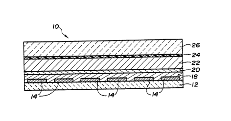
17 An EL laminate 10 incorporating a two layer
18 dielectric in accordance with the present invention is
19 illustrated in Figures 1 and 2. The laminate 10 is
20 built from the rear side on a substrate 12. A rear
21 electrode layer 14 is formed on the substrate 12. As
22 shown in the Figures, for display applications, the rear
23 electrode 14 consists of rows of conductive address
24 lines centered on the substrate 12 and spaced from the
2~ substrate edges. A electric contact tab 16 protrudes
26 from the electrode 14. A first, thick dielectric layer
27 18 is formed above the rear electrode 14, followed by a
28 second, thinner dielectric layer 20. A phosphor layer
29 22 is formed above the secon~ dielectric layer 20,
30 followed by a front, transparent electrode layer 24.
31 The front electrode layer 24 is shown in the Figures as
32 solid, but in actuality, for display applications, it
33 consists of columns of address lines arranged
34 perpendicular to the address lines of the rear electrode
35 14. The laminate 10 is encapsulated with a transparent
36 sealing layer 26 to prevent moisture penetration. An
~93/23972 211~ PCT/CA93/00195
1 electric contact 28 is provided to the second electrode
2 24.
3 The EL laminate 10 is operated by connecting
4 an AC power source to the ele~L-ode contacts 16, 28. An
EL laminate in accordance with the invention has utility
6 as lamps or displays, although it will most frequently
7 find application in displays.
8 It will be understood by persons skilled in
9 the art that further intervening layers can be included
in the laminate 10 without departing from the present
11 invention.
12 A method of constructing a double dielectric
13 layer in an EL laminate, in accordance with the
14 invention, will now be described with preferred
materials and process steps.
16 The laminate 10 is constructed from the rear
17 to the front (viewing) side. The laminate 10 is formed
18 on a suitable substrate 12. The substrate 12 is
19 preferably a ceramic which can withstand the high
sintering temperatures (typically 1000~C) used in the
21 dielectric layer. Alumina is most preferred.
22 Deposited on the substrate 12 is the first,
23 rear electrode 14. Many techniques and materials are
24 known for laying down thin rows of address lines.
Preferably, conductive metal address lines are screen
26 printed from a Ag/Pt alloy paste, using an emulsion
27 which can be washed away in the areas where the paste is
28 to be printed. The paste is thereafter dried and fired.
29 Alternatively, the rear electrode 14 may be formed from
other noble metals such as gold, or other metals such as
31 chromium, Lul.ysLen, molyh~ , tantalum or alloys of
32 these metals.
33 The first dielectric layer 18 is deposited on
34 the rear electrode by known thick film t~hniques. The
first dielectric layer 18 is preferably formed from a
36 ferroelectric material, most preferably one having a
37 perovskite crystal structure, to provide a high
W093/23972 21~ PCT/CA93/00195
1 dielectric constant compared to that of the phosphor
2 layer 22. The material will have a ; n; dielectric
3 constant of 500 over a reasonable operating temperature
4 for the laminate, generally 20 - 100~C. More preferably,
the dielectric constant of the first dielectric layer
6 material is 1000 or greater. Exemplary materials for
7 the first dielectric layer 18 include PbNbO3, BaTiO3,
8 SrTiO3, and PbTiO3, PbNbO3 being particularly preferred.
9 As will be understood by persons skilled in
this art, in choosing a ceramic material (i.e. an
11 electrical insulating material having a melting point
12 which is sufficiently high to allow for the preparation
13 of the other layers of the laminate) for the first
14 dielectric layer 18, one chooses materials known to have
lS high dielectric constants and dielectric strengths.
16 These are intrinsic properties of the materials,
17 however, the values are generally given for bulk
18 materials, which are present in a dense, highly
19 crystalline form. The deposition techniques used can
alter these properties. In respect of the dielectric
21 constant of the material, the thick film deposition
22 techn;ques, followed by high t~- ~~ature sintering, will
23 generally preserve a large particle size (in the range
24 of about 1 micron to about 2 microns) and a high degree
of crystallinity in a dense structure, so as not to
26 significantly lower the dielectric constant from that of
27 the starting material. Similarly, a high dielectric
28 strength is achieved using thick film deposition
29 techn;ques followed by high temperature sintering.
However, the dielectric strength of the layer(s) should
31 ultimately be measured by imposing an operating voltage
32 across the completed laminate.
33 Thick film deposition techn;ques are known in
34 the art, as set forth above. By such t~c-hniques, the
dielectric material is deposited on the rear electrode
36 layer 14 to the desired thickness with generally uniform
37 coverage. Thick film deposition tPc-hn;ques are
~ 93/23972 21 1 ~ ~ 1 1 PC~r/CA93/00195
1 frequently used in the manufacture of electronic
2 circuits on ceramic substrates. Screen printing is the
3 most preferred tec-hnique. C -~cially available
4 dielectric pastes can be used, with the recom -n~
sintering steps set out by the paste manufacturers.
6 Pastes should be chosen or formulated to permit
7 sintering at a high temperature, typically about 1000~C.
8 However, other t~hniques can achieve similar results.
9 one alternate thick film te~hn;que is the use a
dielectric as a "green tape", such that it can be laid
11 down on the rear electrode 14. The green tape comprises
12 a dielectric powder in a polymeric matrix that can be
13 burned out during the subsequent sintering process. The
14 tape is flexible before sintering, and can be rolled or
pressed onto the electrode layer 14. One possible
16 advantage of the green tape over the screen printed
17 dielectric is that it may be somewhat more dense with
18 fewer pores once it is fired. At present, green tape
19 dielectrics are not widely available. Thick film pastes
of the dielectric can also be roll coated onto the rear
21 electrode layer 14, or applied with a doctor blade.
22 More complex te~hn; ques such as electrostatic deposition
23 of a dielectric powder followed by immediate sintering
24 before the powder loses its electrostatic charge may
also by used.
26 As indicated, the first dielectric layer 18 is
27 preferably screen printed from a paste. Depositing in
28 multiple layers followed by sintering at a high
29 t~ _erature is preferred in order to achieve low
porosity, high crystallinity and i~; sl cracking. The
31 sintering t~ -~ature will ~ep~ on the particular
32 material being used, but will not eYce~ the temperature
33 which the rear electrode 14 or substrate 12 can
34 withstand. A t~ erature of 1000~C is typically the
maximum for most electrode materials. The thickness of
36 the first dielectric layer 18 will vary with its
37 dielectric constant and with the dielectric constants
W093/23972 a ~ PCT/CA93/00l95
1 and thicknesses of the phosphor layer 22 and the second
2 dielectric layer 20. Generally, the thickness of the
3 first dielectric layer 18 is in the range of 10 to 300
4 microns, preferably 20 - 150 microns, and more
preferably 30 - 100 microns.
6 It will be appreciated that, in general, the
7 criteria for establ;~hing the thicknecc and dielectric
8 constant of the dielectric layer(s) are calculated so as
9 to provide adequate dielectric strength at minimal
operating voltages. The criteria are interrelated, as
11 set forth below. Given a typical range of thickness for
12 the phosphor layer (d~) of between about 0.2 and 2.0
13 microns, a dielectric constant range for the phosphor
14 layer (k~) of between about 5 and 10 and a dielectric
strength range for the dielectric layer(s) of about 106
16 to 107 V/m, the following relationships and calculations
17 can be used to determine typical thickness (d2) and
18 dielectric constant (k2) values for the dielectric layer
19 of the present invention. These relationships and
calculations may be used as guidelines to determine d2
21 and k2 values, without departing from the intended scope
22 of the present invention, should the typical ranges set
23 out hereinabove change significantly.
24 The applied voltage V across a bilayer
comprising a uniform dielectric layer and a uniform non-
26 conducting phosphor layer sandwiched between two
27 conductive electrodes is given by equation 1:
28 V = E2*d2 + El*dl (1)
29 wherein:
E2 is the electric field strength in the
31 dielectric layer;
32 El is the electric field strength in the
33 phosphor layer;
34 d2 is the thi~nPc of the dielectric layer;
and
36 dl is the thickness of the phosphor.
O 93/239722 1 ~ PCT/CA93/00195
1In these calculations, the electric field
2direction is perpendicular to the interface between the
3phosphor layer and the dielectric layer. Equation 1
4holds true for applied voltages below the threshold
5voltage at which the electric field strength in the
6phosphor layer is sufficiently high that the phosphor
7begins to break down electrically and the device begins
8to emit light.
9From ele~Ll~ ~gnetic theory, the component of
10electric displacement D perpendicular to an interface
11between two insulating materials with different
12dielectric constants is continuous across the interface.
13This electric displacement component in a material is
14defined as the product of the dielectric constant and
15the electric field component in the same direction.
16From this relationship equation 2 is derived for the
17interface in the bilayer structure:
18k2*E2 = k~*EI (2)
19 wherein:
20k2 is the dielectric constant of the dielectric
21material; and
22kl is the dielectric constant of the phosphor
23material.
24Equations 1 and 2 can be combined to give
25equation 3:
26V = (kl*d2/k2 + dl)*E~ (3)
27To ini ; 7e the threshold voltage, the first
28term in eguation 3 needs to be as small as is practical.
29The second term is fixed by the requirement to choose
30the phosphor thickness to -Y; ize the phosphor light
31output. For this evaluation the first term is taken to
32be one tenth the magnitude of the second term.
33Substituting this condition into equation 3 yields
34equation 4:
35d2/k2 = O.l*d~/k~ (4)
36Equation 4 establishes the ratio of the
37thickness of the dielectric layer to its dielectric
W093/23972 2118111 PCT/CA93/00195 ~
1 constant in terms of the phosphor properties. This
2 thickness is determined in~Pp~n~ently from the
3 requirement that the dielectric strength of the layer be
4 sufficient to hold the entire applied voltage when the
phosphor layer h~C~_ ?S conductive above the threshold
6 voltage. The thickness is calculated using e~uation 5:
7 d2 = V/S (5)
8 wherein:
9 S is the strength of the dielectric material.
10 Use of the above equations and reasonable
11 values for dl, k~, and S provides the range of dielectric
12 layer thickness and dielectric constant set forth in
13 this specification and claims.
14 As stated previously, a CDCO~ dielectric
15 layer 20 is not needed if the first dielectric layer 22
16 provides a surface adjacent the phosphor layer which is
17 sufficiently smooth (i.e. a subsequently deposited
18 phosphor layer will illuminate generally uniformly at a
19 given excitation voltage) and is compatible with the
20 phosphor layer 22. Generally, a surface relief that
21 does not vary more than about 0.5 microns over about
22 1000 microns (which equates approximately to a pixel
23 width) is sufficient. A surface relief of 0.1 - 0.2
24 microns over that distance is more preferred. If the
25 first dielectric layer 18 provides a sufficiently smooth
26 surface, but does not provide the desired compatibility
27 with the phosphor layer 22, a further layer of material
28 (preferably, but not n~c~sc~rily a dielectric material)
29 to provide that compatibility may be added, for instance
30 by thin film te~hniques.
31 In the event that the second dielectric layer
32 20 is needed, it is formed on the first dielectric layer
33 18. The second layer 20 may have a lower dielectric
34 constant than that of the first dielectric layer 18 and
35 will typically be formed as a much thinner layer
36 (preferably greater than 2 microns and more preferably
37 2 - 10 microns). The desired thickness of second
~ 93/23972 21~ 811i PCT/CA93/00195
1 dielectric layer is generally a function of smoothness,
2 that is the layer may be as thin as possible, provided
3 a smooth surface is achieved. To provide a smooth
4 surface, sol gel deposition techniques are preferably
used, followed by high temperature sintering. Sol gel
6 deposition t~r-hn;ques are well understood in the art,
7 see for example "Fl~n~ ~ntal Principles of Sol Gel
8 Technology", R.W. Jones, The Institute of Metals, 1989.
9 In general, the sol gel process enables materials to be
mixed on a moleclll~ level in the sol before being
11 brought out of solution either as a colloidal gel or a
12 polymerizing macromolecular network, while still
13 ret~;ning the solvent. The solvent, when removed,
14 leaves a solid with a high level of fine porosity,
therefore raising the value of the surface free energy,
16 enabling the solid to be sintered and densified at lower
17 temperatures than obt~;nAhle using most other
18 ~hniques.
19 The sol gel materials are deposited on the
first dielectric layer 18 in a manner to achieve a
21 smooth surface. In addition to providing a smooth
22 surface, the sol gel process facilitates filling of
23 pores in the sintered thick film layer. Spin deposition
24 or dipping are most preferred. These are te~h~iques
used in the semiconductor industry for many years,
26 mainly in photolithography processes. For spin
27 deposition, the sol material is dropped onto the first
28 dielectric layer 18 which is spinning at a high speed,
29 typically a few thousand RPM. The sol can be deposited
in several stages if desired. The thic-kn~c of the
31 layer 20 is ~ol-L~olled by varying the viscosity of the
32 sol gel and by altering the sp;nning speed. After
33 spinning, a thin layer of wet sol gel is formed on the
34 surface. The sol gel layer 20 is sintered, generally at
3S less than 1000~C, to form a ceramic surface. The sol may
36 also be deposited by dipping. The surface to be coated
37 is dipped into the sol and then pulled out at a constant
W093/23972 2i 1811 ¦ PCT/CA93/00195
1 speed, usually very slowly. The thickness of the layer
2 is controlled by altering the viscosity of the sol and
3 the pulling speed. The sol may also be screen printed
4 or spray coated, although it is more difficult to
control the thickness of the layer with these
6 t~chn;ques.
7 The material used in the second dielectric
8 layer 20 is preferably a ferroelectric ceramic material,
9 preferably having a perovskite crystal structure to
provide a high dielectric constant. The dielectric
11 constant is preferably similar to that of the first
12 dielectric layer material in order to avoid voltage
13 fluctuations across the two dielectric layers 18, 20.
14 However, with a thinner layer being utilized in the
second dielectric 20, a dielectric constant as low as
16 about 20 may be used, but will preferably be greater
17 than 100. Exemplary materials include lead zirconate
18 titanate (PZT), lead lan~hA zirconate titanate
19 (PLZT), and the titanates of Sr, Pb and Ba used in the
first dielectric layer 18, PZT and PLZT being most
21 preferred.
22 PZT or PLZT are preferably deposited as a sol
23 gel by spin deposition followed by sintering at less
24 than about 600~C, to form a smooth ceramic surface
suitable for deposition of the next layer.
26 The next layer to be deposited will typically
27 be the phosphor layer 22, however, as set out
28 hereinabove, it is possible, within the scope of this
29 invention to include a further layer above the second
dielectric layer 20 to further improve the interface
31 with the phosphor layer. For instance, a thin film
32 layer of material known to provide good injectivity and
33 compatibility may be used.
34 The phosphor layer 22 is deposited by known
thin film deposition t~hn;ques such as vacuum
36 evaporation with an electron beam evaporator, sputtering
37 etc. The preferred phosphor material is ZnS:Mn, but
28
2118111
~ ~93/23972 ; PCT/CA93/00l95
1 other phosphors that emit light of different colours are
2 known. The phosphor layer 22 typically has a thickness
3 of about 0.5 microns and a dielectric constant between
4 about 5 and 10.
A further transparent dielectric layer above
6 the phosphor layer 22 is not needed, but may be included
7 if desired.
8 The front electrode layer 24 is deposited
9 directly on the phosphor layer 22 (or the further
dielectric layer if included). The front electrode is
11 transparent and is preferably formed from indium tin
12 oxide (IT0) by known thin film deposition te~hniques
13 such as vacuum evaporation in an electron beam
14 evaporator.
The laminate 10 is typically annealed and then
16 sealed with a sealing layer 26, such as glass.
17 A preferred laminate, from rear to front, with
18 typical thickness values in accordance with the present
19 invention is as follows:
Substrate Layer - Alumina
21 Rear Electrode - Ag/Pt Address lines - 10 microns
22 ~irst Dielectric Layer - Lead Niobate - 30 microns
23 Second Dielectric Layer - Lead Zirconate Titanate - 2
24 microns
Phosphor Layer - ZnS:Mn - 0.5 microns
26 Front Electrode - IT0 - 0.1 microns
27 Sealing Layer - Glass - 10 - 20 microns.
28 In larger EL displays, the thicknesses of the
29 layers may vary. For instance, the sol gel layer
thi~knec.-c is typically increased to about 6-10 microns
31 to provide the desired smoo~hn~cs. Similarly, the IT0
32 layer thickness might be increased up to 0.3 microns in
33 a larger display.
34 In accordance with the present invention the
connection of the front and rear address lines of an
36 electroluminescent laminate to the voltage driver
37 circuit is preferably achieved using the through hole in
38 the rear substrate. Most preferably, the EL laminate
29
WO 93/23972 211~111 PCr/CA93/00195
includes the thick dielectric layer of this invention,
2 although this is not n~ces~:~ry.
3 Voltage driver circuitry includes voltage
4 driving components (typically referred to as high
voltage driver chips), the ouL~uLs of which are
6 ~onn~cted to the individual row and column address lines
7 of the rear and front electrodes in order to selectively
8 activate pixels in accordance with the video input
9 signals. The voltage driver circuitry and components
are generally known in the art. To illustrate the
11 present invention, through hole connections were
12 provided for known packaged high voltage driver chips
13 which are to be surface mounted on the rear substrate by
14 known reflow soldering te~-hniques. Such high voltage
driver chips are known for the conventional symmetric
16 pulse driving schemes and for asymmetric pulse driving
17 schemes.
18 However, it will be realized by those skilled
19 in the art that the particular driver circuitry or
driver components may be varied and as such will
21 naturally affect the patterns of through holes and the
22 circuit patterns provided for connection to the driver
23 circuitry. The invention has application whether the
24 entire driving circuit or only a portion thereof is to
be mounted on the rear substrate. For instance, instead
26 of using the high voltage packaged chips, it is pos~;ible
27 to use bare silicon die (chips) on the substrate using
28 conventional die attach methods, and using conventional
29 wirebonding te~hniques to connect the chips to the drive
circuitry on the substrate. In this case, the driver
31 chips would occupy much less area on the substrate and
32 it would be possible to place all of the drive circuitry
33 on the substrate. The result is an ultrathin display
34 panel that could be interfaced directly to a video
signal and connected directly to a dc power supply.
36 Such displays would be useful in ultrathin portable
37 products that require a display. Of course, the ability
2 ~
1 to mount driving circuitry on the rear o~ the substrate
2 is tied to the overall size o~ the display, a larger
3 display providing more space ~or the drive circuitry
4 directly on the rear o~ the substrate.
The circuit connection aspect o~ this
6 invention is illustrated in Figures 3 - 10. As
7 indicated above, particular through hole and circuit
8 patterns are provided ~or illustration purposes for
9 mounting high voltage driver chips 30 on the reverse
side o~ the rear substrate. The particular chips chosen
11 were Supertex~ HV7022PJ chips to connect to the row
12 address lines 14 and Supertex HV8308PJ and HV8408PJ
13 (Supertex Inc. is located in Sunnyvale, ~ali~ornia) ~or
14 connection to the column address lines 24. The latter
two chips di~er in that the lead pattern o~ one is a
16 mirror image o~ the lead pattern o~ the other.
17 Referring to the Figures, the EL laminate 10
18 is pre~erably, but not necessarily, constructed with the
19 two layer dielectric layers 18, 20 o~ this invention,
and is thus constructed ~rom the rear substrate 12
21 toward the ~ront viewing side. The rear substrate 12 is
22 drilled with through holes 32 in a pattern such that
23 they will be proximate the ends o~ the address lines 14,
24 24 (subsequently ~ormed). Alternatively, additional
through holes could be provided in a spaced relationship
26 along the address lines. This would be use~ul to
27 provide connection to ~ront ITO address lines which have
28 high resistivity. The pattern o~ Figure 4 provides ~or
29 connection to an EL laminate 10 on a rectangular
substrate 12, with row address lines (rear electrode) 14
31 along the longer dimension and column address lines
32 (~ront electrode) 24 along the shorter dimension.
33 The through holes 32 are pre~erably ~ormed by
34 laser. The holes 32 are typically wider on one side due
to the nature o~ the laser drilling process, that side
36 being chosen to be the rear or reverse side to
37 facilitate ~lowing conductive material into the holes.
~ 31
-
W093/23972 211~1 i 1 PCT/CA93/00195 ~
1 The substrate 12 used in the EL laminate
2 should be one which can withstand the temperatures
3 encountered in the subsequent processing steps.
4 Typically substrates used are those which provide
sufficient rigidity to support the laminate and which
6 are stable to temperatures of 850~C or greater to
7 withstand the subsequent firing sintering steps for the
8 thick film pastes and sol gel materials. The substrate
9 should also be opaque to laser light, to allow the
through holes 32 to be formed by laser drilling.
11 Finally, the substrate should provide for good adherence
12 of the thick film pastes used in subsequent steps.
13 Crystalline ceramic materials and opaque vitreous
14 materials may be used. Alumina is particularly
preferred.
16 A circuit pattern 34 of conductive material is
17 printed on the rear side of the substrate 12 in the
18 pattern shown in Figure 5. In this step, the conductive
19 material is pulled through the through holes 32 in a
manner to be discussed. The circuit pattern 34 on the
21 rear side of the substrate 12 consists of rear connector
22 pads 36 around each of the through holes 32, chip
23 connector pads 38 for the outputs of the high voltage
24 driver chips (not shown), further connector pads (not
labelled) for conn~ction to the rest of the drive
26 circuit (not shown), and electrical leads (not labelled)
27 between numerous of the connector pads as shown.
28 The conductive material is preferably a
29 conductive thick film paste applied by screen printing.
Silver/platinum thick film pastes are preferred.
31 To form a conductive path through each through
32 hole 32, a vacuum is applied on the front side of the
33 substrate 12 while the circuit 34 is printed on the rear
34 side. This is preferably accomplished by placing the
substrate 12 on a vacuum table with a master plate
36 having holes drilled in the pattern of Figure 4 between
37 the substrate 12 and the vacuum. The holes in the master
~ ~93/23972 21 ~ 81 ~ PCT/CA93/00195
1 plate are aligned with and somewhat larger than the
2 holes in the substrate 12. The vacuum is not applied
3 until the circuit is printed to ensure that the vacuum
4 is uniformly applied. The vacuum is continued until
5 conductive material is pulled through to the front side
6 of the substrate. At that point, a small amount of the
7 conductive material is pulled through to the front side
8 of the substrate 12 and the through hole walls are
9 coated. The thick film paste is then fired in
10accordance with known procedures.
11Following this step a circuit pad
12reinforcement pattern 42 is preferably, but not
13~c~s~rily, printed as shown in Figure 7. Similar
14conductive materials, printing and firing steps are
15 followed.
16The row address lines 14 and connector pads
1740a and 40b are then formed on the front side of the
18substrate 12, preferably by screen printing a thick film
19conductive paste such as a silver/platinum paste. The
20address line pattern is shown in Figure 6 to include
21rows exten~ing along the length of the substrate 12 and
22ending at the front (row) connector pads 40a. During
23this same step, the front (column) co~ctor pads 40b
24are printed to provide for ultimate connection of the
25column address lines to the driving circuitry via the
26through holes 32. The conductive paste is preferably
27pulled through the through holes 32 as above, with the
28vacuum being applied from the rear, circuit side of the
29substrate.
30While the means forming a conductive path
31through the through holes 32 has been set out above to
32be formed from thick film conductive pastes, the
33con~llctive paths might also be formed as electroplated
34through holes, or as through holes formed by electroless
35plating, as is known in the art, provided the
36electroplated material adheres properly to the substrate
W093/23972 ~ 1 i 8 1 I 1 PCT/CA93/00195
1 and that subsequent layers adhere to the plated
2 conductor.
3 The thick film dielectric layer 18 of this
4 invention is then preferably formed and fired in the
manner set out above.
6 The rear circuit side of the substrate is then
7 preferably sealed, with a rear ~e~l~nt 44, for instance
8 by screen printing with a thick film glass paste,
9 leaving the connector pads exposed for attachment of the
10 high voltage driver chips and connPctor pins 45 to the
11 rest of the driver circuitry (not shown). The sealing
12 pattern is shown in Figure 8.
13 The EL laminate is then completed with the sol
14 gel layer 20, the phosphor layer 22 and the front column
15 address lines 24, as described above. The pattern for
16 the front column address lines 24 is shown in Figure 9
17 to consist of parallel columns across the width of the
18 substrate 12 ending proximate the front (column)
19 connector pads 40.
20 Electrical interconnects 46 between the column
21 address lines 24 and the front (column) co~ector pads
22 40 are provided, if necessary, for reliable electrical
23 con~Pction. These are preferably formed by printing a
24 conductive material such as silver through a shadow mask
25 in the pattern shown in Figure 10.
26 A front sealing layer 26 as previously
27 described is provided to prevent moisture penetration.
28 In accordance with the present invention, the
29 front ITO address lines 24 of the EL laminate 10 are
30 preferably formed by laser scribing. This laser
31 scribing tP~h~;que is set forth hereinbelow in
32 connection with the preferred EL laminate 10 of this
33 invention. However, it should be understood that the
34 laser scribing tP~hnique has broader application in
35 patterning a planar laminate having overlying and
36 underlying layers. In that respect, the ITO and
37 phosphor layers 24, 22 are illustrative of overlying
~ 93/23972 2 ~ PCT/CA93/00195
1 layers which do not absorb the laser light to any
2 substantial extent, and the thick film lead niobate
3 dielectric layer 18 and the sol gel layer 20 of lead
4 zirconate titanate are illustrative of underlying layers
that do absorb the laser light. Other typical materials
6 used as trAnCpArent conductors include SnO2 and In2O3.
7 Generally, in the broad context of the
8 invention, the overlying layer is a material which is
9 transparent to visible light and the underlying layer is
a material which is opague to visible light. The
11 underlying material can then be directly ablated, and
12 the overlying material indirectly ablated, by utilizing
13 a laser beam with a wavelength in the visible or
14 infrared region of the ele~Ll~ -gnetic spectrum. This
laser ablation method has broad application in
16 patterning transparent conductive layers in
17 semiconductors, li~uid crystal displays, solar cells,
18 and EL displays.
19 In order to co,.L~ol the precision and
resolution of the laser scribing (depth and width of
21 cuts), to avoid explosive del~ in~tion of the layers and
22 to minimize interdiffusion between the layers, certain
23 properties of the materials and thicknecc~c of the
24 layers should be observed.
In respect of a two layer laminate, the
26 following relationship should hold:
27 ~u Tu > ~O T
28 wherein:
29 ~u = absorption coefficient of underlying layer;
aO = absorption coefficient of overlying layer;
31 Tu = thi~k~S-C of underlying layer; and
32 To = thi~-knecc of overlying layer.
33 More preferably, the product ~f ~u Tu is very
34 much greater than the product of ~O To~
When there is a plurality of overlying
36 transparent layers and/or a plurality of underlying
37 opaque layers, the sum of the product of ~UTu for each
W O 93/23972 2 1 1 % I 1 1
~ PC~r/CA93/00195
1 layer should be greater than the sum of the product of
2 ~oTo for each layer, i.e.
~; crU; T~,; > ~; ~o To;
If the above relationship is maintained, it
6 should be possible to directly ablate only a portion of
7 the underlying layer, without cutting through its entire
8 thickness, and indirectly ablate through the entire
9 thickness of the overlying layer, in accordance with the
process of the invention.
11 Explosive delamination can result if heat or
12 vapour pressure builds up in the underlying layer before
13 the overlying layer can soften and/or vaporize by
14 indirect ablation. Thus, the material in the overlying
layer should melt and vaporize at a lower temperature
16 than does the material in the underlying layer.
17 To enhance the ability to make high resolution
18 cuts, the thermal conductivity of the material in the
19 underlying layer is preferably less than that of the
material in the overlying layer. The thermal
21 conductivities of both layers should be such that
22 significant heat does not flow away from the region
23 being ablated in the time during which that region is
24 exposed to the laser beam.
To avoid mass interdiffusion between layers,
26 the diffusion time for such processes should be greater
27 than the time during which the region to be ablated is
28 exposed to the laser beam.
29 The above preferred properties are generally
known for materials, making it possible to predict which
31 materials are A ~nAhle to the laser scribing process of
32 this invention.
33 Resolution of the laser cuts, explosive
34 delamination and interdiffusion are also affected by the
wavelength, power and scAnn; ng speed of the laser beam.
36 However if the above relationships and properties are
37 generally maintained, these other laser conditions can
38 be controlled and varied to achieve the desired results
39 of direct and indirect ablation.
36
~ 93/23972 2 1~ 8 1 1 1 PCT/CA93/00195
l Lasers are known which provide a laser beam
2 with a wavelength in the visible or infrared region.
3 Carbon dioxide lasers, argon lasers and YAG lasers are
4 exemplary. All have wavelengths greater than about 400
nm. Pulsed or continuous wave (CW) lasers may be used,
6 the latter being preferred to provide sharp, high
7 resolution cuts. The laser beam is focused by
8 a~. ~r iate known lens systems to achieve the desired
9 resolution and to ensure sufficient local power density
for complete removal of overlying layer. Generally, the
ll power density of the laser beam is set so that the
12 ~Loo~e which is c~t is significantly greater than the
13 thickness of the overlying transparent layers. When the
14 transparent layer comprises electrode address lines,
lS this ensures that the address lines are clearly defined
16 and electrically isolated.
17 Scribing can be performed either by moving the
18 laser beam with respect to the material being scribed or
l9 more preferably, by mounting the material to be scribed
on an X-Y coordinates table that is moveable relative to
21 the laser beam. For scribing address lines, a table
22 moveable in the X direction (i.e. perpendicular to the
23 lines being scribed) is preferred, the laser beam being
24 moveable in the Y direction, i.e. along the lines.
Material which is vaporized or de~o ~ed
26 during the laser scribing process may be drawn away from
27 the material being scribed by a vacuum located proximate
28 to the laser beam.
29 In the preferred EL laminate lO of the present
invention, a thin layer of indium tin oxide 24 is
31 deposited by known methods above the phosphor layer 22.
32 Vacuum deposition methods or sol gel methods to deposit
33 ITO are disclosed in U.SO Patents 4,568,578 and
34 4,849,252. Materials other than ITO may be used, for
example fluorine doped tin oxide. An optional
36 transparent dielectric layer can be provided between the
37 ITO and phosphor layers 24, 22. The preferred sol gel
38 layer 20 of PZT and the thick film dielectric layer 18
39 of lead niobate underlie the phosphor layer. The EL
37
W093/23g72 211~ PCT/CA93/00195
l laminate 10 is formed in reverse sequence to
2 conventional TFEL devices, as described hereinabove.
3 This conveniently leaves the IT0 layer 24 and the
4 phosphor layer 22 as upper (overlying) transparent
layers above lower tunderlying) opaque dielectric layers
6 18, 20 (lead niobate and PZT), amenable to laser
7 scribing in accordance with the present invention.
8 The individual column address lines 24 are
9 laser scribed, as described above. The laser beam
directly ablates at least a portion of the sol gel layer
11 20 and possible a minor portion of the thick underlying
12 dielectric layer 18 and indirectly ablates the IT0 and
13 phosphor layers 24, 22 throughout their thicknesses.
14 This leaves a reliable insulating gap between the
adjacent address lines.
16 The column address lines 24 are connected to
17 the driving circuitry as described above. More
18 particularly, in accordance with the preferred through
19 hole connecting process described above, the electrical
interconnects 46 are formed (prior to laser scribing) by
21 evaporating silver in the pattern shown in Figure 10 in
22 locations to overlap the portions of the IT0 layer which
23 will ultimately form the address lines. The address
24 lines are then scribed in the manner set out above.
The completed EL laminate 10 can be sealed as
26 described above by spraying a protective polymer sealant
27 on the front viewing surface or by hon~ i nq a glass plate
28 26 to the front surface.
29 Several advantages are derived by using
indirect ablation to scribe transparent conductor
31 materials. A relatively low power continuous wave laser
32 producing light in the visible range can be used rather
33 than an ultraviolet pulsed laser with a high
34 instantaneous power output. This not only re~llces laser
costs, but produces smoother edges on the ablated cuts.
36 This is particularly important for high resolution EL
37 displays. Direct ablation of transparent materials
38 requires very high instantaneous laser power to deposit
39 the energy neC~ccAry for the ablation in a time short
38
93/23972 2 ~
PCT/CA93/00195
l enough to prevent diffusion of heat away from the area
2 where ablation is to occur. In prior art attempts to
3 directly ablate a transparent ~on~ctor deposited on a
4 transparent substrate, only a small fraction o~ the
laser power is directly absorbed by the transparent
6 conductor material; most of the light passes through
7 both transparent layers. In many cases, indirect
8 ablation can minimize the problem of interdiffusion
9 between layers, since the heating to vaporize the
transparent layers occurs from the bottom o~ the
ll transparent layers. This promotes the removal of
12 ablated material outwardly and upwardly in the stream of
13 vaporized material, rather than diffusion of the
14 material into the underlying layer. This is
particularly important in order to preserve the quality
16 of the dielectric and phosphor layers in EL displays.
17 The present invention is further illustrated
18 by the following non-limiting examples.
19 EXAMPLE 1
This example is included to illustrate that
21 simply screen printing a thick film layer of barium
22 titanate (the material used as a ceramic sheet in the
23 Miyata et al. references) is subject to electric
24 breakdown under operating conditions of about 200V.
A single pixel electroluminescent device was
26 constructed on an alumina substrate (5 cm square, O.l cm
27 thick) obt~ from Coors Ceramics (Grand Junction,
28 Colorado, U.S.A.). A rear electrode layer was applied,
29 centered on the substrate, but spaced from the edges.
The material used was a silver/platinum conductor which
3l was printed as address lines as is conventional in
32 electronics. More particularly, Cermalloy # C4740
33 (available from Cermalloy, Co~shnho~-ken,~Pa.) was screen
34 printed as a thick film paste through a 320 mesh
stainless steel screen and coated with an emulsion. The
36 emulsion was exposed to ultraviolet light through a
37 photomask, so as to expose those areas of the emulsion
38 that were to be retained for printing. The unexposed
39 emulsion was dissolved away with water where paste was
39
21~811i ~
W093/23972 PCT/CA93/00195
1 to be printed through the screen. The L~ '; n; ng
2 emulsion was then further hardened with additional light
3 exposure. The printed paste was dried in an oven at
4 150~C for a few minutes and fired in air in a BTU model
TFF 142-790A24 belt furnace with a temperature profile
6 as rec- ?n~ed by the paste manufacturer. The maximum
7 processing t~ ,~rature was 850~C. The resulting
8 thickness of the fired electrode conductor layer was
9 about 9 microns.
A dielectric layer was formed on this
11 electrode layer as follows. A dielectric paste
12 comprising barium titanate (ESL # 4S20 - available from
13 Electroscience Laboratories, King of Prussia,
14 Pennsylvania, dielectric constant 2500 - 3000) was
printed through a 200 mesh screen in a square pattern so
16 that all but an electrical contact pad at the edge of
17 the electrode was covered. The printed dielectric paste
18 was fired in air in the BTU furnace with a temperature
19 profile as recommended by the manufacturer (maximum
temperature 900 - 1000~C). The thickness of the
21 resulting fired dielectric was in the range of 12 to 15
22 microns. A second and third layer of the dielectric
23 were then printed and fired over the first layer in the
24 same ~nner. The combined thi~-kn~cs of the three
printed and sintered dielectric layers was 40 to 50
26 microns.
27 A phosphor layer was deposited directly onto
28 the dielectric layer in accordance with known thin film
29 techn;ques. In particular, a 0.5 micron thick layer of
zinc sulphide doped with 1 mole percent of man~n~e was
31 evaporated onto the dielectric layer using a UHV
32 In~ nts Model 6000 electron beam evaporator. The
33 layers were heated under vacuum in the evaporator and
34 were held at a temperature of 150~C during the
evaporation process which took approximately 2 minutes.
36 The phosphor layer was coated with a 0.5
37 micron layer of a transparent electrical conductor
38 consisting of indium tin oxide. This layer was applied
~ 93/23972 21 ~ PCT/CA93/00195
1 by known thin film deposition t~hn; ques, in particular
2 using the electron beam evaporator at 400~C under vacuum.
3 The laminate was subsequently annealed in air
4 for 15 minutes at 450~C to anneal the phosphor and indium
tin oxide conductor layers. An indium solder contact
6 was provided to the IT0 layer. The device was sealed
7 with a silicone sealant (Silicone Resin Clear Lacquer,
8 cat.#419, from M.G. Chemicals).
9 The device was tested by applying a DC voltage
of 200 volts across the two electrodes. The device was
11 observed to fail upon application o~ the voltage due to
12 electrical breakdown of the dielectric layer in the
13 region i -~;ately ~ oul,ding the contact to the indium
14 tin oxide.
Without being bound by same, it is believed
1~ that the failure of the device was because the
17 dielectric layer did not provide the needed smooth
18 surface for the phosphor layer. Microcracks could be
19 observed at the surface. This may, however, be due to
the presence of deleterious materials in the c ~~cial
21 dielectric paste and is thus not an indication that
22 barium titanate cannot be used as a single or first
23 dielectric layer in accordance with the present
24 invention.
EXAMPLE 2
26 This example is included to illustrate that a
27 screen printed dielectric layer from a paste containing
28 lead niobate, a material known to have a high dielectric
29 constant and a lower sintering ~- ~~ature than barium
titanate, provides adequate dielectric strength, but
31 does not luminesce.
32 A device was constructed that was similar to
33 that in Example 1, but having a dielectric layer formed
34 from a dielectric paste of lead niobate, Cermalloy #
IP9333 (dielectric constant about 3500, thicknesc as in
36 Example 1). The device, when tested was not subject to
37 dielectric breakdown when a DC voltage of 400 volts was
38 applied. However, it failed to lum;~ecc~ on application
39 o~ an AC voltage.
41
W093/23972 2118111 PCT/CA93/OOt9~ -
1 Without being bound by the same it is believed
2 that the failure to l~ ineS~ was due to compatibility
3 problems at the interface with the phosphor layer. Thus
4 this example should not be taken as an indication that
lead niobate cannot be used as single or first
6 dielectric layer in accordance with the present
7 invention.
8 EXAMPLE 3
9 This example illustrates a two layer
dielectric constructed in accordance with the present
11 invention, with a first dielectric layer of lead niobate
12 (as in Example 2) and a second dielectric layer of lead
13 zirconate titanate. Favourable luminescence was
14 achieved.
A device identical to that in Example 2 was
16 constructed, but with the additional step of applying a
17 layer of lead zirconate titanate ~PZT) using a sol gel
18 process to the printed and fired dielectric layer before
19 the phosphor layer was applied. The sol was prepared in
the following ~-nn~r. Acetic acid was dehydrated at
21 105~C for 5 minutes. Twelve grams of lead acetate was
22 dissolved into 7 ml. of the dehydrated acid at 80~C to
23 form a colourless solution. The solution was allowed to
24 cool, and 5.54 g of zirconium propoxide was stirred into
the solution to form a pale yellow solution. The
26 solution was held at 60~C to 80~C for five minutes after
27 which 2.18 g of titanium isopropoxide was added with
28 stirring. The resulting solution was agitated for
29 approximately 20 minutes in an ultrasonic bath to ensure
that any r: ~in;ng solids were dissolved. Then,
31 approximately 1.75 ml of a 4:2:1 ethylene glycol to
32 propanol to water solution was added to make a stable
33 sol. More ethylene glycol was added before coating to
34 adjust the viscosity to the desired value for spin
coating or dipping. The prepared dielectric layer was
36 spin coated in one case and dipped in another case with
37 the sol. In the case of spin coating the sol was
38 dribbled onto the first dielectric layer which was
39 spinning in a horizontal plane at 3000 rpm. In the case
42
RC~.~O~:~P~ C~ 4 ~181~1 +49 ~ 4~;#l~
1 of di~ping, a hi~her viscosity 801 was used For the
~ dlpping procedure the substrate was pulled from the sol
3 at a r~te of 5 cm per ~inute. The resulting coated
4 assembly wa~ then heated in air in an oven at a
- ~-temperature o~ 600~C ~or 30 minutes to convert t~e sol to
6 PZT. The thi~kne~ of the PZT layer was approxima~ ely
7 2 to 3 micron~. The ~urf~ce of the P~ l~y~r was
8 observed to be co~iderably ~other than that o_ the
9 screen printe~ and sintered first dielec~ric layer.
Following applie~tion of the PZT layer, the
11 phos~hor and trans~arent co~uctor layer~ w~re deposited
12 ~ in ~Y~ple 1.
13 The co~leted 1,tm; n~tte perfor~ed well with
14 luminosity ~ersu~ voltage characteristics s~milar to c~r
better than those reported ~y Miyata e~ al. The
16 thre~hold voltage for ~n;nlmlmt ll~m;n~nce for the display
17 lwa~ 110 v . Lum~ nosity at 5G volt~; above threshold ~ i . e .
18 160 volt~, 6Q Hz) ~a~ lg4 c~ndelas per square meter (57
1~ ~ot T~rts).
EXAMPLE 4
~1 This exam~le i~ included to illustrate th~t
2~ variation6 in the ~hickness of.the dielec~ric l~er ha~e
23 an e~fect on both the operating ~oltage and ~he
24 ltlmin~nce o~ the display6.
2~ . A displ~y was con~ructed as in Exa~pl2 3,
26 except that only two instead o~ three screen printed
27 layers of dielectric were applied. The thickne6s of the
28 ~irst dielectr~c layer was correspon~;ngly reduced to 25
29 to 30 ~icrons.
The dl8play functioned well. The threshold
31 volta~e for m;~;~t~ m;n~nce was 70 volts ~cp 110 volts
32 i~ Exam~le 3}, expected ~rom theoretical con~ider~tio~s.
33 The l~ no.~i~y at So volts a~ove the threshold ~alue
34 also decressed ~o llg candelas per ~quare meter ~35 ~oot
~berts) (cp 1~4 candel~s per ~guare meter ~57 foot
3~ Lamberts) in Exam~le 3).
37 Exa~ple 5
38 Thi~ ex~mple illust_ates the preferred
3g embo~im~nt of conne~ting the row and column addres~
43
A~END~DSHEET
RC~. VO~::EPA l~ CHE~ 4 :'7~3- 4~ 7 40:34-~94~53-- +49 ~9 ~3~944~;.~:ft'1~;
2~t8~1
1 lines of the EL 1~;n~te to the driver circuit usins
~ thr~ugh hole~.
3 An addre~able -EL display wa~ co~tructed
4 using the same ~equence o~ layer depositions as ~et
.~orth ln Examp~e 3. ~he substrate was a 0.0635 cm
6 ~0 ~25 in~h) thick.rectangle o alumina obtained ~r~m
7 Coors Ceramic~ (Gr~nd J~nction, Color~do, U.S.A.~ ~lavi~s
8 ~ sions of len~th - 15 cm (~ in~h~) and width - 5 cm
~ (2 ~n~h~s}. The ~ubstrate was drilled with 0.015 cm
~0.006 inch~ ~iameter t~rou~h holes usin~ a carbon
11 dioxide laser in the patt~rn shown in Figure 4. The
12 substrate wn~ inspectcd t~ en~ure that ~ll of the holes
13 were clear. The holes wexé ~und to be about 0.02 cm
14 ~0.00$ inche~) in diameter on the 8ide ~acing the laser
an~ about O . 015 cm (~ .006 i~hes) on the oppo~ite ~ide.
1~ The side with the wider hol.e. o~enin~s was cho~en to be
17 the rear side of the ~ub3trate t~ ~acilitate flowing
18 con~ucti~e materi~1 into the through hole~.
19 Followi~g this, the circuit p~ttern ~h~wn in
~igure 5 was printed onto the rear gide of the ~ubstrate
21 through a stainle~s ~teel scree~ with 128 wire~ per
22 centi~eter (32S me~ ~t~inless ~teel screcn) using
23 Cermalloy ~4740 silver platinu~ ~aste. During the
24 printing process, the substr~te wa~ allgned with a
~aster plate having 0.10 cm ~0.040 inch) hole~ drilled
26 in t~e same patter~ as shown in Figure 4 and a v~cuum
27 w~s appli~d below the ~aster plate to pull the
28 c~n~lctive pa~te through the through holes in the
29 . substrate ~i.e. throu~h to the front, ~iewing ~ide of
~he s~bstrate). Th1s ~tep formed the circuit ~attern of
31. Figure 5 to~ether with a conduc~i~e path th~ough each of
32the throu~h hol~s in the ~ubstrate. To ensure
33uIlifon~ity in the application of the vacuum~ the ~acuum
34was not turned on until the ~ubstrate had been printed.
35The part was in~pected to ensure that the through hole~
36were ~illed.
37Following printing, the~ ~ub~:trate was fir~ed in
38a.ir in 1~ BT~ odcl TFF 142-79~A24 belt furn~ce with a
AMENDED SHEET
RC~O.\~:EPA ML~ NCHEN 4 :~9- 4-94; 15:4;3: 40~34~9445~3~ +4~3 ~.'3 ~.~99~4':;5:~1 ~
2118111
temperature prof il.e reco~Lmended by the paste
2 manufacturer. ~he Tr~Yimll~n temperature was 850~C~
3 Following this step, a circuit reinforcement
4 pat tern as shown i~ Figure 7 wa~ printed and i~ired on
the rèar, circuit ~ide of the su~strate ~using the same
6 Cer~lloy conductive paste). Thi~ ~;tep ~d~ th~ circult
7 p~Ltterr~ thicker in certair~ are~ where electrical
8 connections were to :te subse~uer~tly m~de.
9 The row addre~ lines and the ~rorlt row and
colun~ connector pad~ were then screen printed on the
ron~: ~riewing side of the subs~rate. The line~; extended
12 across the len~th of the su~strate to the row ~omlect~r
13 pad~ in the pattern shown in Figu~e ~. The colu~
14 connector pad~;, a~ shown in Figure 6, were printed i~L
thi~ ~ame step. The row sddress lines and connector
16 pad~; were for~ rorn th~ same conductive pa~t~
17 ~Cermalloy #4740~ using the ~ame ~rinting and ~iring
18 conditior~ he sub~trate was po~itioned on the same
19 ~na~;ter plate ~rith the through hole pa~tern of~ Figure ~
2 0 and a vacuum was applied f~om below to Dull ~he
21 conducti~e p~J3te throuç~h the through hole~ towa~d the
22 rear side of the sub~trate. Th~ thickness o~ the ~ired
23 electrode layer was about 8 micrometer~. There were
24 about 20 ~ddress lines per c~n ~5~ address lines per
inch~ . and the total num~r of add~e~3s lines was ~8 . The
26 part was ey:qm; n~ to ens~ure the through holes were
~7 filled.
28 The three layers of the dielectric pa~e
2~ ~Cermalloy #IP9333 were printed and ~ired as set forth
in ~xamp~e 3 to form a d~ielectric layer o~ about 50
31 micrometer~; thickness.
32 ~he rear, circuit s~de~ of the ~substrate wa~
33 then sealed. A thick film glz~s~3 paste ~Her~eus IP9028,
34 from ~eraeus-Ce~alloy, Cor~Rh~lhocken~ Pa. ) was screer~
printed u~;ing a Rcreen with 98 wires per centimeter ~250
3 6 mesh 6creen1 in the ~attern shown in Figure 8 . The
37 conrlector ~ads for connection to the hi~h voltage driver
3~ chip~ ~nd other driver circuitr~r were left uncovere~l.
39 The glas8 ~ealin~ layer was then fired in the Bl'U belt
AMENDE~3 St~EET
RC~ ~O;~ E~'A ~I[:E.:\iCllE~ 4 . ~- 4-~34: 15:4~3: 4~ 445;3_ +49 8~ 944~S:~
~ 2~8~1
1~urnace u~ing a temperature profilQ recommended by the
2m~nu~acturer with a ~Ytm~lm temperature o~ 700~C.
3Duri~g the aboYe mentio~ed firing steps, the
4substrate wa~ ~u~orted on ~ie~es of ceramic material at
5---~ither.end to avoid contact between the printed material
6on the circuit side and the belt of the ~urnace.
7The sol gel layers were then formed by dipping
8~bstantially as set out in Ex~ple 3. Three o~ fo~r
g~ol gel layers were typically ~sed, with pulling rates
10o~ 4 - 10 sec~cm ~10 - 25 sec~in) from a mixture having
11a vi~coslty o~ about 100 cp as measured by the falling
12ball visc~eter. ~etwaen dip~ng layer~, the ~1 g~l
13was drie~ at 110~C for 10 min. A vacuum chuck was placed
14aver the active area of the lA~;n~te and the ~ol gel was
lSwater washed off the r~inins area~. The l~yer was
1~then ~ired at sbout 600~C i~ a belt furnace ~or 25 min.
17A total ~l gel thicknes~ botween 3 - 10 microm~tres was
18achieved. This wa~ followed b~ ~he phosphor layer o~
19Example 3 using zinc su~ide doped with 1~ ma~gane~e
20with a thickness of 0.5 - 1.0 micrometers.
21The column address lines were then deposited
~ro~ indi~m tin oxide, a~ d~scribed in Exampl~ 3, in th~
23pattern shown in Fi~ure 9. There were about 20 column
24a~dress l~nes per cm (52 colu~n addre~s lines per inch~
25and a to~al of 256 columns. The spacing ~etween the
26lines wa~ 0.00~5 cm (0.001 inche~ and ~he line width
27was 0 05 cm (0.019 inche~ (center to center~.
28Silver was ev~porated through ~ ~hedow ma~k in
29the pattern ~hown in Figure 10 to make the ele~trical
~0connections o~ the column ad~ress lines to the column
31connector pads and throu~h h~le conductors ~n the
3~ ~u~strate.
33The ~i~wing surfac~ o~ the l~;~.te w~s sealea
34with a silicone sealant sprayed ove~ the entire front
35face o~ the di~play. The sealant usea was Silicone
36Resin Clear Lacguer, ~at. #419 from M.G. Chemlcals.
37The comple~ed display was tested by connecting
38a ~ulse gcnerator pro~iding a 160V ~quare wav~ ~ignal at
3960 Hz acro~s pairs o~ row and column pads on the circui~
4~
AMENDEO SH~ET
RC~ 'O,~ A ~ iCHE.~ 4 :5~9- 4-94 ~ 4;3: 4()34-'944;>3-- +4~ 89 ~~3~~9~465:#1'~
~ 211811~
depc~ited on the re~r of the subs~rate. Ea~h pixel o~
:2 ~he di~3play was found to light up independelltly and with
3 a consi5tent inten5ity e~al to that me;~sured in Bxa~zple
4 3 when the voltage w~s applied. No dy~unctio~al pixels
--were ;E.o~lnd among the total pixel count of 17408.
~XAMPhE 6
7 This ex~nple illu~trates the ~referred
8 ernho~ ent of laser scribin~ the indium tin oxide
9 addre~s line~ o~ t~e EL 1 Am;n~3te o~ the present
inve~tion.
address~able matrix ~isplay wa~; construc~ed
1~ on a ceramic su~strate using the f ollc~wing procedure .
13 The su~str~t~ was a 0.0~4 c~m ~0.025 inch) thic3c
14 rectangle o~ alumina wi~h length 15 csn (6 inchest and
1~ width 5 cm ~:~ inches ~ obt~ inerl ~ronL Coor~ Ceram~c~
16 (Grand Junction, ~olorado, U. S.A. ) . Thi~; was drilled
17 with û . ~15 c~n ~0 . 006~ inch dla~nete~ holes with a carbon
18 dioxide l~er in ~he ~a~tern shown in Figure ~. ~he~
19 part Was in~pected to ensure that all o~ the holes w~re
2 0 clear .
21 Following this ~;tep~ the circui~ pattern sh~wn
22 in l~ e 5 wa~ printed through ~ stainless ~it~el screen
~3 with 128 wires Per cm (325 mech E;tainless ~;teel ~:creen)
24 usin~ C~-11OY ~C~h~ho~k~ Penn~ylvania, U,S.A.~
#4740 ~ilver ~latinum pa~e. Duri~g the printing
2~ ~roce~s, the ~ubstrate was aligned with a master plate
27 having 0.10 Gm ~0 04~ inch~ hole~ drilled in the ~a~e
2~ pattern as the sub#trate to facilitare app~ying a vacuu~
29 to the substr~te hole~ during prin~ing. The vacuum
~ucked pa~te throu~h the holes to facilitate the
31 for~ation of a con~uctive p~th through the ceramic
~2 sub-~trate after the p rt wa~ fired. The part wzs ~ired
33 in ~ir i~ a BTU model qtE'F 142-7gOA24 belt furnace with
34 a temperature profile rec~r~ y the p~te
manufa~turer, having a ~ximum tempexature of 850JC.
36 Following thi~ ~te~, a circuit reinforcement
37 pattern as ~hown in Figur~ 7 was prin~ed ~nd ~ired on
38 the re~r, circult ~ide o~ ~he substrate (using the same
39 C~rmalloy conducti~e paYte). This ~e~ made the circ~it
47
AMEI~Jn.~
.
RC~ O~i: EPA ~ !\ICHEI~: 4 : "9 - 4 - 94 : 15: 44 : 4()~ 944.~i3_ 1 4~ 89 '':~9944 ~;5: t~ ''0
-' ~ 2118111
pa~tern thicker in cert~n area~ where electrical
2 connection6 were to be ~ ec~uently ma~e
3~ Follclwing thi~, a set o~ row addres~ line~ and
4 co~ector pads were printed on the fron~ ~riewing side of
. the substrate. The line~ extended along the len~th of
6 the substrate to th~ ro~ connector pads (~8 sh~wn in
7 Figure 6 ? . ~he colulr~ connector pad~ were aiso for~ned
B in this ~cep ~as shown in Figure 6). ~he row address
g lines and the row and ~olumn connect~r p~ds were ~ormed
~rom the same ~i~ve~ platinum paste u~ing the same
11 printing and firing-conditions. ~he ~ubs~rato wa~
12 po~itioned on the ~e ~ter ~late with the through
13 hole pattern of Fi~ure 4 and a vacuum was applied from
14 }~elow ~o pull the conductive ;7aste throu~h the throug~
holes toward the rear Sia~ of the subs~rate. The
16 thic~nes~ o~ the fired electrode layer was abou~ 8
17 micro~eters. ~here were 2~ addre~s lines per cm (52
18 addre~ lines per inchj and the total ~ e~ ~f address
19 lirles was Ç8.
2 o Next three layers o~ lead niobate ~ielectric
21 ~ paste ~cerTn~llo~r #IPg3~3) were se~uenti2~lly printed and
~:~ fired ir~ the belt ~ur~ce with ~ te~perature pro~ile a~;
~3 reco~m~n~ed by the manu~acturer ~ m t~mper~ture
24 850C) on top o~ the row addres~ lines (as set ~orth in
Example 31. The co~bined t~;~knecs o~ the dielectric
~6 layers was 50 micromeSer~
27 Following this, the r¢~, circuit sid~ o~ the
28 ~ub~trat~ was ~ealed as ~et ~orth in Exa~ple 5, in the
2~ pattern ~hown in Figure 8.
Next, a 3 - 1~ ~icrometer thick la~er ~f lead
31 zirconate titanate ~P~) was depo~ited on the lead
32 niobate layer to form ~ ~mooth surf~ce. Th~ sol gel
33 te~hni~ue using dipping, a~ se~ out in Example 5, wa~
34 used. A thin film pho~hor layer was then de~osited
u~i~g electron be~m evaporation methods as k~own in the
3~ art. The phosphor layer was zinc ~ulfide doped with 1%
37 manganese, which ~as ~epo~itod to a thickn~ss ~f be~ween
38 0.5 and 1 ~icr~eter~.
.
4~
AMEND~O SHEET
.. . . ~ - .
~C~ C~:~A h~ lC~F3~; 4 :~9- 4-94 ~ 44: 4034~.94~5~3 1 +4~ ~39 ~399~4~;5:#~
~ 2118111
. .
.
The n~ct ~;te~ was to deposit a 300 ~ metre
2 thick layer o~ indi~n tin oxide ~TO) o~ the pho~phor
3 layers u~ing electron beam e~aporation meth~d~ as known
4 ._ in the art.
This ITO layer ~ra5 then patterr~ed into 2S6
6 addre~s line~ using ~ 2 Watt CW (continuous wave) arçron
7 ion la~er tuned to a wavelength of 514.5 n~nnln~tres.
8 ~he EL lamin~te ~a~ mo~tea on a ~oveable X coordinate
9 table, w~ich moved the laminate in a direction
perpendicular to the lines bein~ ~cribed beneath the
11 laser bea~. ~e la~er beam was mo~ed in the Y ~irection
12 to scri.be the line~. The la~er ~eam was ~ocussed to
13 li! micromete~ ~ps:~t a~d the laser power was adju~ted BO
14 that the indium ti~ oxide, t~e underlyiny pho~;phor laye;c
and about 10~ o~ the combined ~nderlying dielectric
16 la~ers were ablated awa~ where ~he la~er beam had
17 ~c~n~ (about 1.8 W~. The ~cA~n;~ speed w~
18 controlled ~t ~bout 100 and soo mm~sec to pro~ide
19 addre~s line~ with about 40 ox 25 micr~metres gap
, re~pecti~ely and addres~ line de~th of 6-8 or 3-4
21 micro~etxe~ respectively. The spacing betwee~ addr~s6
22 line~ Ii.~. between ~en~r~s of the lines) was about 500
23 micr~meters. A vacuum adjacent th~ ~ubstrate withdrow
24 vaporized an~ ablated materia~. The pattern of ~he
transparen~ electrode~, o~ce ~he ablation was completed,
2~ was a~ ~hown in Fi~ure 9. On the completed dis~lay,
~7 there were ~bout 20 colum~ add~ess lines per cm ~50
28 column addre~~ lines ~er inch) ana a total of 256
2g c0~ 8.
Prior to scribing the ITO column addre~s
31 lines, the ~ilver interconnects between the front
32 (colu~n~ connector ~ad~ and the ~lt~mate ITo addres~
33 lin~s were scr~en ~rin~ed ~ro~ silver throu~h a shadow
34 mask ~n the patter~ of ~igure 10.
After laser ~c~ibing, the ~ro~t ~iewing side
36 of the com~le~ed dixplay w~s sprayed with ~ prc~e-ti~e
49 .
AMEN~ED SHEET
RC~'~YO.~ A M~IEI~CHF-'N 4 :~'9- 4-~34: 1~:44: 40;34 94453 ~ +49 89 ~ 994~65:#"'
~ 2 1 ~
1 polymer co~tin~ ~Silicone Resin Clear ~ac~uer, c~t ~41g
2 from M~ ~hemic~ls).
3 ~he di~play was then tested ~y applying a
4 ~oltage ~cro~s selected pixel~ by connecting ~ pulsed
power supply provi~ing voltage pulse~ of 160 volt~ at a
6 repetition rate o~ 64 Hz. Th~ pixels each lit llp
7 reliably with a lumino~ity ~imilar to th~t of the single
8 pixel device ~f t~ previou~ example.
S The resolution o~ the adare~s lines ~ this
example i~ generally much hi~her than is achievable with
11 ~tate o~ the art ~hotolithographic technique~
12 Com~ercially available ~evices typically have ITO
13 addre~:s lines with widths o~ 180 - ~ OS microm~ters and
14 ~p~ ~etween the lines of 65 - 80 micrometer~. As set
out a~over in ~cordance with this invention, gaps of 25
1~ and 40 mi~lo~,a~ers were produced, dep~n~;n~ on ~he laser
17 ~c~nn; n~ ~peed. This higher resolution allows ~or 2
18 hi~her ratio of ~ctive to total area o~ the di~play,
19 ~ince wider ITO ~ddre~ lines with smaller gaps c~n be
~0 , u6ed.
21 EXAMPLE 7
2~ Thi~ example illu~trate~ a ~wo 12yer
~3 dielectric con~tr~cted in accord~nce with the present
24 invention but with the first dielectric layer beiny
constructed from a pa~te ha~ing a higher dielectric
26 constant th~n the paste u~ed in Examples 3 and 4.
27 ~he device was constructed as set forth in
28 Exam~le 3 r ~ut h~ing ~ fir~t dielectri~ layer ~or~ed
~9 ~ro~ a lead niobate ~ste ~vailable from Electros~ience
Laborat~rie~ ~s a hi~h ~ c~Ac;tor pa~te under the
31 numb~r 4210. ~e sintered p~ste has a dielectric
32 constant ~f abou~ lO,Ooo. ~h~ ~irst dielectric layer
33 h~d a thickness of about 50 microns. A ~ol gPl layer of
34 PZT w~ a~lied, as d~cribed in ~xam~le 3, to a
thick~e~s o~ about 5 micron~. -
A~END~0 SHEET
~C~ ,P~ SC~ 4-~14 : 15: 45 ; 4()34~>94453~ +49 89 ~3994 ~;5: #~73
~ 211~111 ,~r
The de~rice ~unctioned well with a threshold
2 l.raltage for rr;n;ml~m lllml n~nce of 91 Volt~; and ~L
3 lum~nosity at 150 ~olt~; of 170 candelas per scauare meter
~ 5 0 i~ot Lam}~ert~3 ) .
EXAMPLE 8
6 This example illustrate~ a two layer
7 cielectric: con~2truct~d wit~ a first diel~3ctric layer
8 ~ormed from a l~d niob~te p~ste and a second die.lectri
9 laye~ formed fro3n lead lanth~tlm zirconate titarlate
(PLZT) . P~T ha~ a dielectric c~onstant of a~out lr ~~~ ~
11 ~he P~ZT had a molar ratio of zlrconium to titanium to
12 laIlthAnl~m of 52: 3~ :16 .
13 ~he d~3vice wa~ c:or~6tructed as ~et forth i~
14 ;3xaI~Iple 3, with the sol gel layer being pre~ared as
follow~:
1~ Into 50 ml of q7 acial acetic acid was
17 di~;solved 120 ;7r~ns of ~ . 596 purity lead acetate . The
18 resultin~ solution wa~ heated to 90~C and held at thi~
19 te~Lperature ~or Z minutes before being cool.od to 70~C.
Next, 55.4 gram~; o~ zirconium PLU~OXide W~S added arld
2 ~ l:he resulting ~olution was heated to ~0~C and held at
2~ that temperature for ~ minute. After cooling to 70~C,
23 21. 8 ~rams of titani~n i~o~ropoxide wa3 add~d. Next,
24 11. 4 grams of lAnth~lum nltrate was dissol~re~ in 20 ml
~5 of slacial acetic acid, and thi~ was added to the
.~6 solution. Finally, to stabilize the solution an~l adju~t
27 the visco~;ity to a ~uitable ~r~lue, 10 ml of 6~thylene
28 glycol, 5 rnl of propan-2-ol ~nc~ 2 . 5 ml o~ demineralized
29 w~ter were added.
3 0 The PLZ~ sol gel w~ ~pplied to .the f irst
31 die~ectric layer by dipping in a manner slmilar to ~hat
3~! describe~ in Exan~le 3. The dipp~2d parts were :Eired at
33 600~C to convert the 8econd layer to PLZT. Four ~O~I~S of
34 PLZT were applied by succ~8~ive dippin~ and firing in
thi~; way to prep;~re ~ ~;urface of ade~uate ~oothness ~or
36 the de~osition of the phosphor layer. ~ tot~1 thickne~;s
37 oi~ 5 Inicron~ was achieYed.
S1
Ah1END~ ~CHFFT
~ 2 ~ ~ 8 ~
2 _ v
3 The device ~unctioned well with a threshold
4 voltage of 75 Volts and a luminosity of 94 candelas per
s~uare meter (37 ~oot Lamberts) at 150 Volts.
6 The terms and expressions used in this
7 specification are used as terms of description and not
8 o~ limitation. There is no intention, in using such
9 terms and expressions, of excluding equivalents of the
~eatures shown and described, it being recognized that
11 the scope o~ the invention is de~ined and limited only
12 by the claims which follow.
52
~r