Note: Descriptions are shown in the official language in which they were submitted.
-1- ' '
DIGITAL CURRENT REGULATOR
BACKGROUND AND SUMMARY OF THE INVENTION
This invention relates to AC drives and, in
particular, to a device and method for regulating the
current supplied by an inverter to an induction motor in
response to switching signals from a waveform generator.
Given that motor currents must be accurately
controlled to eliminate the risk of inverter trips, it is
necessary to eliminate or reduce the disadvantages of
current control. These disadvantages include the need for
more voltage headroom on the inverter bus, less than
optimum inverter switching signals, poorly defined switch~
ing frequency, and significant errors in current regulation
at high stator frequencies.
There are several basic approaches toicurrent
control. Control of current in the stationary reference
frame using bang-bang control or triangular modulated
control is the most common. The characteristics of these
regulators have been studied and they are known to require
a great deal of voltage headroom and to result in large
current errors under some circumstances.
The next level of control is to regulate the
; currents in either a stationary or synchronous reference
frame by taking into account that only seven discrete
voltage vectors can be applied to a motor. At each sample
interval, a~new voltage vector is chosen based on the
present current error and an estimate of back EMF. In
general, these schemes require some sort of comparator
which chooses different voltage vectors under rapidly
changing dynamic conditions than the voltage vectors which
' would be chosen to correct only small current errors. In
this way, the available inverter switching frequency is
better utilized. However, these schemes are subject to
loss of current control if orientation is lost.
For optimum current control, a current regulator
is provided to generate voltage magnitude and phase
information which is supplied to a conventional voltage
3 ~ ~;;S~I i
0
mode PWM waveform generator which chooses multiple voltage
vectors to generate the required average voltage. This
technique provides optimum inverter gating signals. When
s combined with a digital control system so that the regulat-
5 ed current reaches its set point in one sample time, the
current regulator provides excellent dynamic current
control without the need for a large voltage headroom.
Limiting of the demanded motor voltage based on the known
constraints of the available inverter bus voltage and the
10 PWM waveform modulation index provides a further decrease
in the necessary headroom.
Brief Descri~tion of the Drawinqs
The drawings illustrate the best mode presently
contemplated for carrying out the invention.
Fig. 1 is a block diagram of an AC drive incorpo-
rating the digital current regulator of this invention.
Fig. 2a is an electric schematic of an integrator
shown in Fig. 1.
Fig. 2b is an electric schematic of an analog to
20 digital converter shown in Fig. 1.
Fig. 3 is an electrical schematic of the signal
generating hardware of a waveform generator shown in Fig.
1. ,
Fig. 4 is a timing diagram showing the input and
25 output signals associated with the signal generating
hardware of Fig. 3.
Detailed DescriPtion of the Preferred Embodiment
This invention relates to AC drives and, in
particular, to a device and method for regulating the
30 current supplied by an inverter to an induction motor in
response to switching signals from a waveform generator.
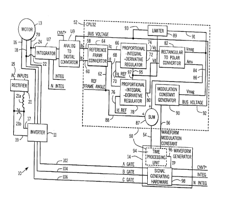
Fig. 1 is a block diagram of the AC drive,
generally designated by the reference numeral 10, for use
in conjunction with this invention. The AC drive 10 is
35 comprised of an inverter 11, a waveform generator 14, and
an AC motor 13. The AC drive system 10 converts three-
phase, 60 hertz input power, 15, to an adjustable frequency
'~:
and voltage source for controlling the speed of the AC
motor 13. Bus lines 16, 18, and 20 interconnect the motor
13 and the inverter 11.
The AC input power, 15, is converted to a DC bus
voltage across lines 17 and 19 by rectifier 21. The
voltage across lines 17 ancl 19 is inputted into inverter
11. Inductor 21a and capacitor 21b filter the bus voltage
from rectifier 21.
Current feedback, lines 22, 24, of two motor
currents is required for the instantaneous current regula~
tor. The electrical schematic of the current sensor and
the integrator is shown in Fig. 2a.
The output values of the integrator, U7, are the
average analog values of the current feedback of two motor
currents for the first half of a carrier cycle. The
carrier cycle is defined as the period of the reciprocal of
the switching frequency of the inverter.
Upon receiving a sample signal, CNVT*, from the
waveform generator 14, the analog to digital converter, U9,
converts the analog current feedback signals to digital
current feedback signals, Ib and Ic. In addition, the
analog to digital converter, U9, generates a digital bus
voltage signal.
The digital current feedback signals, and the
digital bus voltage signal are input into a microcon~
troller, 50, incorporating a CPU32 core, 52. The CPU32
core, 52, generates a space vector waveform angle, line 54,
and a modulation constant, line 56. The space vector
waveform angle, line 54, and the modulation constant, line
56, are sent to a time processing unit, 94, incorporated in
the microcontroller, 50. The time processing unit, 94, is
programmed to generate the timing signals necessary to
implement a space vector PWM waveform algorithm. The PWM
waveform algorithm provides lower current ripple and better
utilization of available inverter bus voltage than do
alternative PWM waveforms.
, ~.
a
.. .
4 -
Referring to Fig. 2a, a current sensor transform-
; er 23 is provided. As :is known, the current sensor
transformer, 23, senses the phase currents on lines 18 and
20 from inverter 11 to motor 13. Current sensor transform-
er 23 provides a first phase current, line 25a, to pin 4 of
a current sensor header, J2. The first phase current
passes through a burden resistor, R2, and continues out pin
5 of header J2 back to the current sensor transformer 23 on
line 25b.
The current sensor transformer 23 provides a
second phase current on line 25c to pin 6 of current sensor
header ~2. The second phase current passes through a
burden resistor, R3, and continues out pin 7 of header J2
on line 25d to the current sensor transformer 23.
A commercially available integrated circuit chip,
TL052A, having two differential amplifiers, U5A and U5B, is
provided. A positive twelve volt power supply is connected
to pin 8 of the TL052A chip. A capacitor, Cl6, decouples
the positive twelve volt power supply. A negative twelve
volt power supply is connected to pin 4 of the TL052A chip.
A capacitor, C17, decouples the negative twelve volt power
supply.
An amplifier circuit is formed with resistors R4,
R5, R8, and R9 in conjunction with differential amplifier
U5A in order to amplify the voltage across burden resistor
R2. Likewise, a second amplifier circuit is formed with
resistors R6, R7, R10 and Rll in conjunction with differen-
tial amplifier U5B in order to amplify the voltage across
burden resistor R3.
The output of differential amplifier U5A, pin 1
i of the TL052A chip, is a first phase current signal, Ibp.
The output of differential amplifier U5B, pin 7 of the
TL052A chip, is a second phase current signal, Icp.
An ADG444 commercially available integrated
circuit chip, having four switches, U6A, U6B, U6C, and U6D,
is provided. Pin 1 of the TL052A chip is connected to pin
3 of switch U6A of chip ADG444 through resistor R12. Line
U
5 -
30 interconnects an inverter protection circuit, 31, which ~ ~
is known, to pin 1 of the TL052A chip at node 32. ~ -
Pin 1 on switch U6A is connected to receive an
integrate signal, INTEG, line 34. Pin 2 on switch U6A is
connected to pin 2 on a differential amplifier, U7A. Pin
6 on switch U6B is connec:ted to pin 1 on differential
amplifier U7A through resistor R13. Pin 7 of switch U6B is
connected to pin 2 of differential amplifier U7A at
junction 38. Pin 8 on switch U6B is connected to receive
a reset signal, N INTEG, line 36.
Pin 9 of switch U6C is connected to receive an
integrate signal, INTEG, line 39. Pin 7 on differential
amplifier U5B is connected to pin 11 of switch U6C through
resistor R15. Line 40 interconnects inverter protection
15 circuit 31 and pin 7 of differential amplifier U5B at ~'
junction 42. Pin 10 of switch U6C is connected to pin 6 on ~ ;
differential amplifier U7B.
Pin 16 of switch U6D is connected to receive a
reset signal, N INTEG, line 44. Pin 15 of switch U6D is
connected to pin 10 on switch U6C and to pin 6 on a
differential amplifier, U7B. Pin 14 on switch U6D is
connected to pin 7 on differential amplifier U7B. Capaci-
tor C2 interconnects pin 6 on differential amplifier U7B ~"
and pin 7 on differential amplifier U7B. Pin 5 is connect-
ed to ground through resistor R17.
Differential amplifiers U7A and U7B comprise an
integrated circuit. The integrated circuit is commercially ;
available under the part number TL052A. -~
Referring to Fig. 2b, a commercially available
analog to digital converter, U9, available under the part
number AD7874, is provided. Pin 1, Fig. 2b, on the analog
to digital converter, U9, is interconnected to pin 1 on
differential amplifier U7A, Fig. 2a, by line 45. Pin 2,
Fig. 2b, on analog to digital converter U9 is connected to '
pin 7 of differential amplifier U7B, Fig. 2a, by line 47.
Pin 3 of analog to digital converter U9 is connected to a
five volt power source, VCC. The five volt power source,
. ~ ,. .
5 ~ :
- 6 -
VCC, is connected to ground through capacitors C3 and C24.
Pin 9 of analog to digital converter U9 is also connected
to the five volt power source, VCC. Pins 23 and 14 of
analog to digital converter U9 are grounded.
Pin 8 of analog to digital converter U9 is
connected to pin 1 of a commercially available negative
five volt power supply, MC79LO5, U10. Pin 1 of power
supply U10 is also connected to pin 26 of analog to digital
converter U9 and to ground through capacitors C4 and C5.
10Pins 2, 3, 6 and 7 of negative power supply U10 are
connected to a negativé twelve volt power source. In
addition, pins 2, 3, 6, and 7 are connected to ground
through capacitor C6. Pin 5 of power supply U10 is
connected to ground.
15Pins 24 and 25 of analog to digital converter U9
are tied together. Pin 28 of analog to digital converter
U9 is connected to pin 1 on header component JPl~ Pin 2 on
header component JP1 is grounded. Known circuitry within
the AC drive 10 senses the bus voltage from the inverter 11
to the motor 13 and provides the value of the bus voltage
with respect to ground to header component JP1 such that
header component JP1 may sense the value of the bus
voltage.
Pins 10-13 and 15-22 on analog to digital
converter U9 are connected to lines DO-D11 of a bus line,
D. Pins 6 and 7 of analog to digital converter U9 are
connected to line CS*5 of a bus line, CS*, and pin 4 of
analog to digital converter U9 is connected to line IRQ*5
of a bus line, IRQ*. Pin 5 of analog to digital converter
U9 is connected to receive a sample signal, CNVT*.
Bus lines D, CS*, and IRQ*, connect to a commer-
cially available MC68332 microcontroller, 50. The micro- ';
controller 50, Fig. 1, incorporates a CPU32 core, 52, which
is programmed to implement the current regulator of the
invention. The CPU32 core accepts the bus voltage and the
motor current feedback from bus lines D and CS*, Fig. 2b,
and generates a space vector waveform angle, line 54, and
~i
i 7
a modulation constant, line 56. The space vector waveform
angle, line 54, and the modulation constant, line 56, are
; sent to a time processing unit, 94, incorporated in the
MC68332, 50. The M~68332 time processing unit, 94, is
programmed to generate the timing signals necessary to
implement a space vector PWM waveform algorithm. The
timing signals are sent to programmable logic arrays U8 and
U19, Fig. 3, on bus line TP, 96. The programmable logic
arrays, U8 and U9, are commercially available under part
number 22V10.
Referring to Fig. 3, pins 2 - 10 of programmable
logic array U8 are connected to lines TP0 - TP8 of bus line
TP. Pins 11 and 13 of programmable logic array U8 are
connected to pins 23 and 22, respectively, of programmable
logic array U19. Pin 1 of programmable logic array U19 is
connected to line TP0 of bus line TP. Pins 5, 6, 7 and 8
of programmable logic array U19 are connected to lines TP9,
TP10, TP11, and TP12, respectively. Pin 21 of programmable
logic array U19 is connected to pin 14 of programmable
logic array U8.
Upon receiving the timing signals on bus line TP,
switching signals, A gate, B gate and C gate on lines 102,
104 and 106, respectively, are generated by programmable
logic array U8. In addition, programmable logic array U8
generates the above noted integrate signal, INTEG, the
reset signal, N INTEG, and the sample signal, CNVT*.
In operation, current feedback is accepted by
current sensor transformer 23, Fig. 2a, from two of the
three motor signal phases from the inverter 11 to the motor
13. The first phase current is processed through differen-
, . .
tial amplifier U5A in order to amplify the signal, Ibp. ~
Similarly, the second phase current is processed through ~ -
differential amplifier U5B in order to amplify the signal,
Icp.
Because the signal from the inverter 11 to the ,~
motor 13 employs three different voltages to synthesize the -
required instantaneous voltage, the phase current signals,
'. ~,. ';
', ~','
''-' ' '
,~ ~ 0
8 -- !
,.
Ibp and Icp, will rise or fall at three different rates
during the carrier cycle. Therefore, the instantaneous
current at a given point in a carrier cycle will not be an
accurate representation of the fundamental component of
current which the regulators are supposed to be control-
ling. However, the fundamental component of current may be
calculated based on the following conditions or assump-
tio~s.
1. The motor back EMF or speed voltage is not
changed significantly during a carrier cycle;
2. The second half of the carrier cycle applies
the same average voltage to the motor as the first; and
3. The average current during the first half of
the carrier cycle may be sampled or calculated.
The average current during the first half of the
cycle is calculated by integrating the current during this
half cycle and dividing by one half of the carrier period.
The output of differential amplifiers U5A and U5B
are inputted into analog switches U6A and U6C, Fig. 2a,
respectively. Analog switches U6A and U6C are used to
apply phase current signals, Ibp and Icp, to integrators
U7A and U7B. Analog switches U6B and U6D reset the
integrators U7A and U7B in response to a reset signal, N
INTEG, at lines 36 and 44 after the phase current signals,
Ibp and Icp, are sampled by analog to digital converter U9,
Fig. 2b, in response to a sample signal, CNVT* at pin 5.
Upon an integrate signal, INTEG, at lines 34 and
39, integrators U7A and U7B begin to integrate phase
current signals, Ibp and Icp, respectively. At approxi-
mately the end of one-half of the carrier period, the
waveform generator, 14, Fig. 1, sends the sample signal,
CNVT*, to pin 5 of the analog to digital converter, U9,
Fig. 2b. Upon sending the sample signal, CNVT*, the
waveform gen~rator, 14, ceases to send the integrate
signal, INTEG, thereby opening analog switches U6A and U6C.
Because switches U6A and U6C are open, integrators U7A and
U7B are in a hold mode, so the output levels at pin 1 of
- 9 - ~
integrator U7A and at pin 7 of integrator U7B remain
constant.
Upon receiving the sample signal, CNVT*, the
analog to digital converter U9 converts the integrator U7A
output at pin 1, the integrator U7B output at pin 2, and
the bus voltage at pin 28 into a digital signal at pins 10-
13 and 15-22 of the analog to digital converter, U9. This
digital signal, representing the phase current signals, Ibp
and Icp, and the bus voltage, is transferred to the
microprocessor 50, Fig. 1, on lines D0-D11 of bus line D in
response to an interrupt signal sent on line IRQ*5 of bus
line IRQ* to signify that the analog to digital conversion
is complete. When microprocessor 50 receives the interrupt
signal, line IRQ*5, it generates a reset signal, N INTEG,
at lines 36 and 44 which opens analog switches U6B and U6D
and resets integrators U7A and U7B.
Referring now to Fig. 1, the digital current
signals representing phase current signals, Ibp, Icp, on
bus line D are shown as Ib, line 58, and Ic, line 60.
Digital current signal Ib, line 58, digital current signal
Ic, line 60, and reference frame angle, line 62, are input
into a reference frame converter 64.
~ .:
As is known, a three-phase motor may be mathemat- '~
.;;~. ~:
ically represented as a two-phase motor having two axes of
magnetic symmetry. The axis in which the magnetic flux is
generated is known as the direct axis. The axis perpendic-
ular to the direct axis is known as the quadrature axis.
These expressions, direct axis and quadrature axis, are
normally shortened to D-axis and Q-axis.
Using the two digital currents, Ib at line 58 and
Ic at line 60, and the reference frame angle, line 62, the
reference frame converter calculates the quadrature axis
current, Iq, line 66, and the direct axis current signal,
Id, line 68. The Q-axis current signal, line 66, and a Q-
axis current reference signal, Iq ref, line 70, are
inputted into a proportional-integral-derivative regulator
72.
.~ ~ 0
1 0 -- '
As is known, a proportional-integral-derivative
regulator takes the difference of the inputs and generates
an error signal which is a linear function of the inputs.
This error signal is input into the integral portion of the
regulator which, in turn, generates a second signal which
is proportional to the time integral of its input. The
second signal and the error signal are multiplied by
separately adjustable gains and the results summed.
The derivative portion of the regulator takes the
difference between the previous input signal to the
regulator and the present input signal to the regulator and
multiplies the difference by an independently adjustable
gain. The output of the proportional-integral-derivative
regulator is obtained by summing the output of the deriva-
tive portion of the regulator with the previously obtainedsum generated from the second signal and the error signal.
The output of proportional regulator 72 is the Q-axis
voltage signal, Vq, line 74. A digital control system is
incorporated into the conventional proportional-integral-
derivative regulator, 72, so that the current regulatedreaches its set point in one sample time. This is known as
a deadbeat controller.
A first order model of a motor from the point of
view of the current regulator consists of a simple R-L
(Resistance-Inductance) series circuit. At typical carrier
frequencies and for current step changes approximating the
rated magnetizing current of the motor, the resistive term
becomes insignificant.
A deadbeat controller for motor current may be
implemented if the inductance is known. For a step current
change, ~I, and a sample time, T, an applied voltage,
L~I/T, applied for one sample time will cause the motor
current to exactly reach its set point. Thus, a propor-
tional gain term of L/T will prove to be the optimal
35 regulator gain. -
The deadbeat concept can be incorporated into a
conventional proportional-integral-derivative regulator by
using the calculated gain as the proportional gain. The
integral gain is then chosen to adequately compensate for
errors which are introduced by the resistance and any back
EMF terms. The derivative term is used to estimate the
average feedback current during the entire carrier cycle
based on the average current sampled in the previous and
the present sample times.
The current regulator can be self-tuning by
applying a known voltage significantly greater than the
expected IR drop to the motor for one sample time and
observing a change in current. The subtransient inductance
of the motor can then be calculated. This value may be
used in other calculations or adaptive regulators, particu-
larly, in estimating rotor time constant or flux level in
field orientation algorithms.
The D-axis current signal, line 68, Fig. 1, and
a D-axis current reference signal, Id ref, line 76, are
inputted into proportional-integral-derivative regulator
78. The output of proportional-integral-derivative
regulator 78 is the direct axis voltage signal, Vd, line
80. A digital control system is also incorporated into
proportional-integral-derivative regulator 78.
The Q-axis voltage signal, line 74, and the D-
axis voltage signal, line 80, are inputted into a rectangu-
lar to polar converter 82. The rectangular to polarconverter, 82, converts the Q-axis voltage signal, line 74,
and a D-axis voltage signal, line 80, from rectangular
coordinates to polar coordinates. The output of rectangu-
lar polar converter 82 is a voltage magnitude signal, Vmag,
line 84, and a voltage angle signal, Amv, line 86.
The reference frame angle, line 88, is added at
~l ?r 87 to the voltage magnitude angle signal, line 86,
to produce the space vector waveform angle, line 54. The
voltage magnitude signal, line 84, is fed into a modulation
constant generator, 90. The modulation constant generator,
90, divides the voltage magnitude signal, line 84, by the
.~
' : :
O
12
bus voltage, line 92, to produce the modulation constant,
line 56.
It is important to utilize as much of the
inverter's voltage capability as possibleO The excitation
signals from the inverter to the motor experience satura-
tion characteristics at modulation constants above lØ As
- a result, stable operation a1: high output voltages requires
that the integrators in the current regulators be clamped.
The integrators in the regulators, 72 and 78, are clamped
by a signal, lines 95 and 97, respectively, from a limiter
89. The limiter 89 observes the voltage magnitude signal,
line 91, and the bus voltage, line 93, and generates the
signal, lines 95 and 97, to clamp the regulator outputs in
proportion so that the integrators demand the maximum
allowed voltage magnitude without varying the voltage angle
signal. Clamping adjusts the integrator value so that
transient conditions caused by integrator overshoot are
avoided.
The clamping level is based on the bus voltage
feedback, line 93, and is set to allow a 3-5% inverter
headroom. The levels to which the separate integrators are
clamped are based on their proportional contribution to the
voltage magnitude, i.e., after the clamping action, the
voltage magnitude is reduced, but the voltage angle signal
remains the same.
The waveform angle, line 54, and the waveform
modulation constant, line 56, are inputted into the time
processing unit, 94, of the microprocessor 50. The time
processing unit, 94, generates TPU signals on bus line TP, ;
line 96, wherefrom the signal generating hardware, 98,
' constructs the control signals, CNVT*, INTEG, and N INTEG,
and the gating signals, A gate, B gate, and C gate.
Referring to Fig. 4, the sync signal, TP0,
defines on its rising edge, 97, the beginning of a carrier
cycle, and on its falling edge, 99, the half point of the
carrier cycle. On rising edge 97 of sync signal, TPO, the -~
integrator signal, INTEG, l0l, goes low. The integrator
' .
,,,~,;
- 13 -
signal, INTEG, 101, is sent by the waveform generator 14 to
line 34 connected to pin 1 of switch U6A and to line 39
connected to pin 9 of switch U6C, Fig. 2a. A low at pin 1
of switch U6A and at pin 9 of switch U6C causes switches
U6A and U6C, respectively, to close. With switches U6A and
U6C closed, Fig. 2a, integrators U7A and U7B integrate the
phase currents, Ibp and Icp, respectively.
On falling edge, 97, of the sync signal, TPO, the
integrator signal, INTEG, 101, goes high. At rising edge
10 103, the integrator signal, INTEG, 101, opens switches U6A
and U6C, Fig. 2a. With switches U6A and U6C open, the
values at pin 1 of integrator U7A and at pin 7 of integra~
tor U7B remain constant. With the values at pin 1 of
integrator U7A and at pin 7 of U7B being constant, a sample
signal, CNVT*, lG5, is sent to pin 5 of analog to digital
converter U9, Fig. 2b. The sample signal, CNVT*, is
.. . .
concurrent with the falling edge, 99, of the sync signal,
TPO.
When the analog to digital converter, U9,
completes converting the analog inputs at pins 1, 2 and 28
to the digital outputs at pins 10-13, 15-22 of analog to
digital converter U9, the reset signal, N INTEG, 107, goes
low, as shown by falling edge 109. The reset signal, N
; INTEG, 107, is sent from the waveform generator 14, to line
25 36 connected to pin 8 of switch U6B and to line 44 connect-
ed to pin 16 of switch U6D. When the reset signal, N
INTEG, line 107, goes low, switches U6B and U6D close,
thereby resetting integrators U7A and U7B so that the
outputs at pin 1 of integrator U7A and at pin 7 of integra~
tor U7B are cleared. The outputs at pin 1 of integrator
U7A and at pin 7 of integrator U7B remain clear until the
reset signal, N INTEG, 107, goes high, thereby opening
switches U6B and U6D. The rising edge 112 of reset signal,
N INTEG, 107, coincides with the rising edge, 97, of the
sync signal, TPO.
Typical gating signals, A gate, B gate, and C
gate, 114, 116, 118, respectively, are shown. The gating
,' ~ ''
- 14 -
signals, A gate, B gate, and C gate are derived from the
time processing signals, lines TP0-TPll, as is known.
Lines 102, 104 and 106, Fig. 1, transmit the gating
signals, A gate, B gate and C gate, from the waveform
generator 14 to the inverter 11.
It can be seen from the above description that
various alternative embodiments are possible without
departing from the spirit of the invention.
~:' .' '
''',; ~"'''',~
;":,., ',".'."'
~,i,' ~','~
., ' . ' ....