Note: Descriptions are shown in the official language in which they were submitted.
:. ~
Po~a~ 8upply Co~rol ~o~ ceiver
~io~ o~ tho ~v0~tl0n
The present invention r~la~ss to a powe~ Cupply control and,
~ore p~rti~ularly~ to a power ~upply control for a ~elective
calling receive~ having a batt~ry saving ~unction.
D~ipt~ t~o ~ a ~t
In a prior art ~elective calling receiver, a co~troller
~upplies a ~attery current to a receiving portion therein only
wh~n the rece~ver receives a synchronizing ~ignal and a ~ra~e
ass~gned to it~ ow~ recei~r to reduce con~umpti~n of the
battery. Namely, the receiving po~tion i~ turned on only at each
timing o~ the sy~chroniz~ng ~ignal and the asslgned fra~e and is
turned ~ at other times.
H~wever, ~ince ~everal receiver~ are a~signe~ to one f~ame,
~S ~he frame may not in~lude ~ messag~ for the receiver lf ~he
receiver turns the receiving po~tion on at a timing ~f the
as~igned ~am~. Ther~o~, an imp~ove~ receiver i~ dl~clo~ed in,
for ~xample, Jap~ne e P~tent Laid-Open Applic~tion No.
115632~1992 ~JP 04~115632.~ ~hi~ recei~er d~tects whether a
, 20 me~sag~ addre~ed to it~ bwn receive~ i5 includ~d o~ not and
turns ~he ~ecei~ing portion o~ ediately aft~r determinin~
that the addres~ed message i~ not included in the ~ram~
While ~uch a r~ceiv~r can reduce con~umed current, ~ince th~
receiver turn~ the ~eceiving portion on at a t~ming o~
~ .~ '.,.
'''''''`'',"''''',
,:,', '',''""' ~:
each synchronizing s~gnal, the re~eiver ~t~ll con~umes too much
cu~rent an~ therefore the battery life i~ unneces~arily
ghorten~d .
~ 5r ~ EN~
It is there~ore an object o~ ~he p~sent invention to
p~ovide a selective c~ ng recelver which enhances the battery
saving efficien~y by improving the ~eceiving opera~ion ~or the
synchronizing signals ~n~ the ~ra~e~ ~hich are a~6igned to the
receiver.
Anvther o~jec~ of th~ pre~ent inventi~n is to provide a
selective ~alling receivsr cap~bl~ o~ reducing the required
capacity o~ the battery.
It i6 fur~her ~bject of the pr~sent invention to provi~e a
selective calling re~ei~r ~apable of u~in~ a s~all slze battery.
It i3 6till ~ur~her ob~ect o~ t~e present invention to
provi~e a minia~urized selective calllng recel~er.
In a selective calling reoeive~ ha~ing a battery saving
~un¢tion whiah catrie~ out recepti~n in th~ groups ~r frames
a6~igned to the recelver lt~ out of re~eived ~nals
consisting of a plurality of blocked e~ror correction code
sequence~ the pre~ent invention i~ equipped with ~ir~t ~etecting
me~n3 f~r ~e~ecting a ~irst ~nchr~nizing signal follow~d a
. preamble ~ign~l ~ro~ a received signal and fir-Rt control means
~or ge~erating a fir~t timing ignal at the timing ~ group3
Z5 as~igned to the rec:eiver within the received ~ignal, and for
turning a radl~ section in the receive~ on ~n re~ponse to the
~irst timing sign~l and ~or ke~ping the radio s~ction o~ ~t
reception timing~ of syn~hrohizing ~ignals after the dete~tion
the ~irst synchronizihg ~ignal.
According to the present inventio~, the battery saving
ef~ioiency is enhanced by not turning the radi~ section on at ~he
timing~ of the ynchronizing signals following th~ detection of
a ~ir3t synchronizing signal, but by turning on the radio section
only at th~ f~ame~ assigned to the r~ceiver itself, and, dur$hg
the reception, immediately turnlng off the power 3upply o~ the
radio section wh~n it own select~ve ~alling nu~ber or ID is not
found in the ~econd word o~ the frame.
~ s~Ip~Io~ oy ~ RA~Nes
ThR ab~ve a~d ot~r objects, feature~ and advantage~ of thi~
in~ent~on will become more apparent from the followiny detailed
description taken with the accompanying drawing~ in whi~h:
~IG. 1 i~ a ~l~ck ~iagra~ o~ a pxeferred embodi~nt of the
present i~vention; ~ .
FIG~. 2(a)~2(~) illustrate ~ POCSAG for~at ueing in the
present invention;
~Gs. 3~a)-3~d) illu~trate ~iming ch~rts to explai~ a
battery saving operation ac~or~ng to the present invention; ~;
FIG. 4 i~ ~ bloc~ diagram o~ a pre~erred embodiment o~ the
~eco~er shown in FIG. l;
FIG. 5 i~ a~bloc~ diagram of a pre~erred embodiment of the ::
6ync~onization control cir~Uit ~hown ih FI~. 4; and
2~ FI~. 6 i~ a block ~agra~ o~ a prefe~red e~bodi~ent of the
~attery ~aving contl-o} c~rcuit shown in ~IG. 4.
. ; . ~. . . ::: , ' ~ - , : : , ,
;, ''': ' ', ' ::, '' ' ~ ," -
In th~ drawi~gs, t~e sam~ re~e~ence nu~erals denote the 6ame
~tructural elemen~s.
~C~pT ~ ~
~ ow a prefer~ed embodiment o~ the pre~nt lnvention will be
~escr~bed in detail with reference to ~IG~. 1 to ~
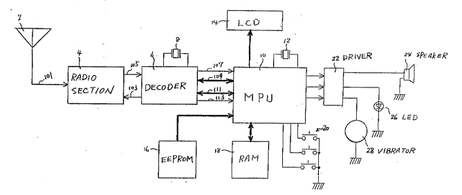
F~G~ a ~l~ck diag~a~ ~ a pre~erred ~mb~diment o~ the
present inv~ntion. A modulat~d F~ignal 101 received ~m an
~htenna 2 i~ demod~lated in a ~adlo ~ection 4. ~he radio section
4 carrles out inte~mittent receiving operation in acco~danc~ with
lo a battexy ~a~ing control ~ignal ~03 o~ a decod~r 6. A
microproce ~or (referre~ to a~ ~PU he~eina~ter) 1~ rea~ a
selectiv~ calling numbe~ or an ide~tification nu~ber (ID) of th~
receiVer itsel~ set in advance in an EEPROM 16, and sends the
~elective calling number to ~he decoder 6 using an addre~s bus
109~ The decoder 6 compare~ the ~electivs calling n~mbe~ ~rom
the ~EPROM 16 with a sign~l 105 demodulated in the radi~ section
4, and informs the MPU 10 ~ th~ detection o~ the selective
oalling number using ~n MPU int~rface, namely, an lnterrupt
sign~l 10~, the addresc bus 109 and a data bu6 111, i~ the re~ult
Z~ of the c~mparison show~ coincidence.
~ IG3. Z~a) to 2tC) illu~tra~e a ~ignal format, prop~e~ hy
a post t~flce code ~tandardization advi~ory gro~lp (POCS~G), which
. ~
i~ u~e~ with th~ pre~ent invention. In FIG. 2ta), the POCS~G .. ;
signal fo~mat i~ constituted of ~ p~e~le sig~l which is a
repeat signal o~ "1" and "~ and w~ich con~ists of 576 ~its, and ~:`
a plurality o~ ~at~he~ each con~i~t~ng of aisynchroniziny ~i~nal
SC and a plurality of line~ of ccde words including a selectlve `~
. .
' ' ~
"",," ,",~,, ","" ~, -, ," ,~'",, ; ',,
;~ ~
calling ~ignal, a me3~age signal ~nd the like. As ~hown in FIG.
2~b), the batch i~ divided into the sC and ~ group o~ eight
frame~ where each group comprises two cod~ w~rds . Each code
word h~ Z1 bits ~ ~n~ormativn, 10 cheok b~t~ f~r c~eck ahd a
parity bit as shown in FIG. ~(c~.
RetUrned to FI~. 1, after ~he coincidence o~ the ~elective
calling number, e~ror correctiQn of diata, ~uch a~ the eheck bits,
sent follo~ing the ~elective o~lling ~ignal i~ carried out, and
t~anæfers ~he in~o~mation bit6 to ~P~ 10 u~ing the MPU interface
for ev~y code word.
The MPU l~ ~eceives the detect~on informati~n on the
~elective calling number ~rom the decoder ~, and store~ the
d~tection inf~rm~tion in a RAM wi~hin MPU ~r an ex~ernal RAM 1~.
I~ therea~ter -aignal6 are sent continuously from ~he decoder 5,
the ~PU 10 ~udges whether the ~ignal~ a~e a piece of meYsage
information si~nals or the selective calling numb~r, an~ the
piece o~ the me3sag~ ormation ~ignals are stored in the bu~er
area o~ the RAM within MP~ or within the external RAM 18 if they
repre~ent n piece o~ ~he ~es~age info~maticn signal~. This
operation is pr~cessed ~y ~PU 1~ u~ing an oscillator ~ as the
~perating clock. I~ the ~ignal-Q t~rn out t~ be the ~elective
calling numb~r, ~ignal acquisition i3 ~tcpped at that moment, an
MPU ope~ating cl~ck ~ an o~cillator 12 is actuated, and the
~ignal~ ac~umulated~o far in the bu~er are procs~ed ~sing the
MPU operati~g cl~ck lZ to be convert~d to a ~e-~sage, for example,
character data and th~ signal~ are storsd in the ~e~sage me~ry
a~ea within the external R~M 18.
After completion of messaye signal reception, MPU 10
notifie~ th~ u~er of the ~eoeiver ~f the ar~ival of a call by
driving a ~peaker 24, an LED 26 or a vibrator 28 via a driver Z2,
~hd d~play~ the contents of the received message on an ~D 14.
5 Which one of the spe~ker 24, L~D ~6 and vibrator Z8 i~ to ~e used
~or the notificatlon is 6et bePore hahd in the ~EPROM 16, and i~
determined by the combination of a t~iece o~ information and the
setting o~ a funotlon ~witch Z0.
~he me~sage ~tored in the R~M wlthin MPU or in the external
RAM 18 can ~e di~played again on th~ LCD l~ by m~ans of the
function ~witch 20.
FIG~. 3(a) to 3(d) illustrate ~ received ~ignal and a timin~
chart o~ battery ~aving operation accordin~ to the pres~nt
inventi~n. In ~IG. 3ta), katch~d parts a~ pre-a signed group3
each o~ wh~ch con~i~ts of two code word6.
~ I~. 3(b~ i}lustrate3 a timing cha~t of the timings o~ the
batte~y saviny control ~ig~al 103 wh~ch carrie~ out the ~es.~a~e
receivi~g operatlon o~ the r~dio ~ection 4, dccoder 6 and MPU 10.
After the preamble ~ignal i~ detected and then the ~ynchronizing
signal SC i~ detected, th~ radio se~tion is turned on exclu~ively
at the timingC oE the code ~o~d~ o~ the group which i~ a~signed
to it~ own receiver, prePe~ably, i4 turned ~n befGre the timing
of the yroup 30 a~ to recei~ the fir~t blt o~ th~ g~p.
! ~ Acco~dinyly, the radi~ ~ection 1~ put to the o~f-state at ~he
25 ti~ings o~ the ~ynchronizing sign~l~ sc that appear later.
Moreove~, during thF reception c~ the code words oP the group
wh~ch i~ as~ighed to th~t re~eiver, the radio ~ection is bro~ght
to the o~f stat~ in the midst of the ~ec~nd e~de word as s~on as
the d~coder det~ct~ that the o~n ID i~ not ~ound.
Fu~the~more, when the rec~ive~'~ ID is detected in the code
word of the group which 19 a~igned to the receiver, two code
w~rds are ~ully received by keeping the on-~tate a~ 1~, then MPU
1~ read~ ~he ~e~sage ~ignal from the dec~der 6 at t~e timing of
the interrupt ,3ignal 107 shown in FIG. 3(c), and 3to~e-~ the
meæ~age ~ign~l in the buffer ~mo~y.
FIG~ 3(d) illustrat~q the o~clllat1on timings of the MPU
1~ operating clock o~ the 06cillator 12. The high level in the ti~e
chart represents that the ope~atl~g clock i5 oscilla~ed the~e.
With this timing, MPU 4 p~oce~3e~ the m~s~age ~ignal within the
buff~r ~mv~y u~ing the ~PU operating clock lZ a~ the working
clD~k, and store~ tne mes.~age signal in the message memory aY a
c~ara~ter data.
~ ext, an example of circuiting for ~xec~ting the above-
mentioned ~attery -~aving operation according to the pre~nt
invention will be de6~ribed in detail with re~erehce to FIGs. 4
to 5.
~0 FIG. ~ i~ a ~lock diagram o~ pr~er~ed e~bod~ment o~ the
decoder 6 ~hown in ~IG~ 1. A bit ~ynchronizing c~rcuit 62
generat~s a regenerat~d clock 125 using re~e~ence clock fro~ an
o cillator ci~cuit 80 and th~ de~dulated signal 105 ~ro~ the
radio ection 4.
~5 A ~a~d rat~ monitor circuit 64 compare~ the regenerated
cl~ck 125 with the de~vdulated signal lOS to d~cide whether it
is a bit ra~e o~ a POCSAG 6ignal to be rec~ived, and output~ a
b~t r~t~ det~ction ~ignal 121. It i~ u~ed in actua~ing th~
7 ~ ~ '
" ' .
operation o~ a seareh ~or the SC ~ignal ~rom the battery saving
oper~tioh in a state where a POCSAG siynal is not beihg received,
and can be used f~r relea~ing the battery ~aving ~pera~ion even
for a ~iign~l other than the preamble ~ignal.
A prea~ble and SC detection circ:uit 66 generates a deteetion
~ignal 117 which detect~ the prea~ble sign~l by sampling the
demodulated sighal lOS u~ing the ~elgenera~ed clock 1~5. As it
detects the ensuing ~ynchronizing signal SC, it generates a
~ynchronization detection sign~l 119.
1~ A ~ynchron~atien oontrol c~rcuit ~B controls the
e~tablis~lment/releasing o~ synchronization~ In the state where
a POCS~G ~ignal i~ not being received, it is engaged in the
battery ~aving operation ~or preamble ~ea~ch mode, and output6
co~inuo~3 reception ~ignal 137 to ~eep the ~adio ~ection in
; :.' . '
the receiving condition by recQiving the pre~mble detecti~n
signal 117 or the bit rate detection signal 121. The
synchronization control circuit 68 i~ brought tG the
synchronizing state by the synch~onization detection signal 119
to re~ume the b~ttery ~a~ing oper~tion ~or selective calling
ZO nu~ber search mode, and receive~ the ~el~ctive calling num~er at
the timings of the pre-a~signed group. The ~ynchroni~tio~
control circuit 58 outputs a group timing .~ignal 115 at th~ pre-
a~igned group and a word ti~n~ nal 123 during the
I synchrlonization ~tate. In addition, the circuit 68 outputs the
Z5 continuou~ xscep~ion ~ignal 137 for receiving the ensuing ~essage
signal by receivinS~ a coin~idence detec~ion ~ignal 129 from a
selective callirlg llu~ber d~ecti~n circuit 7~ o b~ described
later. Fu~ther, the circu~t 68 count6 ~3CH e~r~r detection ~f
:,,
consecutive two cod~ wor~ in i~6 own group by an error checkin~
signal 133 from a B~H error correction circuit 72 to be described
l~er, and goes over to the preamble ~earch mode by relea3ing the
synch~onization ~tate when a count rleache~ a predetermine~ level.
~he ~elYctive calling cod~ de~ection circuit 70 se~uehtially
collate~ the recei~ed ~el~ctive calling number with a pre-
as~ighed selective calling nu~ber 139 vi~ an MPU interface
circui~ 74 from the MPU lo at the timing~ of the group timing
~ignal 115 from ~he ynchronization contrGl circuit 6B, and
~utput~ the coinc~snce dstection ~ignal 129 to the
~ynchron.~zation control circult 68 and an MPU interface circuit
?4. If non-coincidence, pre~erably of more than two bits, i
~et~cted, the selective calling numbe~ det~ction circui~ 7D
immediately outputs a non-coincidence d~tection siynal 135 to a
battery .~aving cuntr~l circuit 76.
~he ~H errcr correction circuit 7z car~ie~ out error
. correction o~ th~ de~dulated signal 105 ~ the timing6 o~ the
~ord ti~ing ~ignal 123 from the ~y~chronl~tion control circuit
6~ and output3 a ~essage ~ign~l 131 to MPU 10 v~a the MPU
~o interface circuit 74. In addition, it checks the errcrs in the
cod~ wo~d received in the ~ynchro~ization statet and outputs an
err~ check ~ignal 133 to the synchronization control circuit ~8.
The ~PU inte~ace c~rcuit 74 controls the MPU interface such
. as ad~ress bu~ 1~9 and data bus 111, and contr~l~ signal
input/output fo~ MPV 10~ .
~he batte~y ~aving control circu~t 76 holds for the duration
~} one word th~ error checking ~ignal 133 of the BCR error
"
correction circuit ~Z at the timings o~ the group ti~ing ~lgnal ~ -~
-.. . ~
115 and the wo~d timi~g signal 123 from the ~ynchronizat~on
cohtrol circuit 6~. when ~he ~attery ~aving con~rol circ~it 7 6
receive~ the non-c~incidence det~ction ~ignal 135 f or the
selective calling number in the ~econd word of its own group, it
immediately turns o~f the power s~pply o~ the radio ~ectl~n 4 by
controllihg th~ ba~tery saving c~ntxol ~ignal 103 i~ the held
cont~nt~ o~ the ~CH ~ck i~ the first word on its o~n group
show that an er~or ~a~ not det~cted.
An interrupt co~rol circ~lt 78 output~ an interr~pt signal
107 to the MPU 1~ ba~d on an inte~rupt req~est signal 127 from
the MPU interface cl~cuit 7i ~hen there aros~ a change in data
to ~e ~ent to MPU 10 or in the operating conditionc. ~he
oscill~tion circuit ~ generate the reference clock 113 by an
o~cilla~or 8.
~IG. 5 i~ a block diagram o~ a preferred embodiment of the
~ynch~oniz~tion control circuit 6~ ~hown in ~IG. 3. A 32-ary bit
count~r 8Z counts the regenerated clock 125 fro~ the bit
synchronizing circUit 6~ and generates the word timing ~ign~l 123
whlch determines the referene tim$ng of one ~ord. A 17-ary ~ord
counter 84 generate~ a timing ~ignal for 17 word3 corresponded
t~ 1 ba~ch length. A ~el~ group timing ~ignal generat~ng circuit
88 generate~ a group timing ~lgnal 115 at the timing of the pre-
a~signed group a~ter a predeter~ d te~m pa~6~d f~om a detection
of ~ynchronizi~g slgnal and a~ the ~iming o~ ~he pre-assigned
gr~up in the ~ollowing bat~h a~ter a detection ~ th~ sel~ctive
calling numbe~ or example, the ~elf group timing ~ignal
g~nerating circuit compr~es ~ compari~on ~ircuit. The
comp~rison circ~it compares the value o~ the counter 84 with a
p~edetermined value showing a positlon o~ the group as~igned to
the receiver and generates the group timing ~ignal when the
value are coin~ident. ~ synchroni2ed ~ate con~l clrcuit 86
control~ the synch~onized state Using th~ preamble detection
~iynal 117, the bit x~te det~ction ~iynal 12t, the ~ynchronizing
signal detec~ion .~ignal 119, the error checking ~ignal 133 and
the s~l~ctive calling numb~r c~incid~nce detection signal lZ9 as
the actuating ~ignals, and generates the continuou~ reception
~ignal 137 and a reset ~ignal to the 3Z-ary and 17-ary bit
countRrs 82 and 84 in respon~e to the synchronizing ~ignal
detection signal l~g.
~IG. 6 i6 a block ~iagram o~ a preferred ~mbodiment of the
battery ~ving control circuit 76 shown in FIG. 3. The circuit
76 ccnsi~ts o~ AND gate~ 90, ~2 and 94, an OR g~te 96, and an
in~erter ~8 ~nd a latch 100 ~or an er~or ch~ck signal holding
mean~. The latch 100 latches the er~or checki~g ~ignal 133 of
the ~cH e~ror correction ci~c~it 72 at thc ti~ing of the
~nputting o~ the 6elf group timin~ ~ignal 115 from ~he
synchronization cont~ol circuit 68 and the word timing ~ignal
lZ3, and hold6 th~ erro~ checking ~ignal 133 for the du~ation o~
one word. ~ the non-~oin~denae detection signal 135 of the
selective calling 5~gnal at the ~econd wo~d of its o~n gro~p and
the latched error checking 6ignal are input to the A~D gate 92,
~e circuit 76 imme~ately turn~ o~ the power supply o~ the
~5 ~adio ~ection 4 at the second word of its own gr~up by
controlling the battery ~aving control signal 103 ~hen the ~el~
group timing signal 115 or c~ntinuou~ reception ~ignal 137 i~
~upplie~ to the AND gat~ 94 via the OR gate 9~
11
Th~ref~re, ~ccording to this selective c~lling receiver ~
the pre~ent invention, a~ter the detection o~ the pre~mble and
the ~ynchronizing ~ignal SC ~n the preamble and SC dete~tion
circuit 66, t~ bits ~n the se:Lective calling number are
se~u~ntially compæred with the pre-as~igned ~elective calling
number in the ~elective calllng code detection circuit 70
exclu~ively at the timing~ o~ the gxoups, na~ely, the code wor~s
a~Yigned to the r~ceiver itself, by th~ ~y~chronization control
~ircuit 6~ The ~elective calling numbe~ detection circuit ~0
detect~ immediately ~electiv~ calling number non-colnci~ence and
outpUt3 a numbe~ non-coin~idence signal when there occurred non-
coincidence of bits ~o~ a num~e~ of times th~t exceed~ a
p~edetermined levsl. Mo~eover, ~elect~ve calling nu~b~r
c~incidence i5 detected and ~ number coi~cidenGe signal i~ output
~hen hon-coinci~ence occurred only ~or a nu~ber o~ bits small~r
than th~ pred~termine~ levelO
In the battery 6aving contrPl circuit 76, the re~ult oE the
block error checking output at th~ completlon o~ ~ne block of the
error ccrrection ~de and received by the BCH error correction
oi~cuit 7a iæ held ~or at lea~t the duration of on~ block. The
pow~r 6upply for the radio section 4 is controlled in ~e~pon~
to the error non-dete~tion output o~ the error check output
holding ~n~ ued in the p~ece~ing block, and ~he n~n-
oinci~ence o~put in the block ~n question.
~5 A~ de cribed hereinbefor~, ~inc~, according to the pr~ent
inven~ion~ ~he radio section ~ turned ~n only in the ~rames or
groups which are pxe-a~igned to the receiver, without turn~ng
the ~dio ~e~tion ~n at the timlngs of th~ synCh~niZin~ ~ignal~
lZ
:
a~ter the synchronizing si~nal is detected once, and the power
supply for the receiving circuit i~ turned of~ lmmediate~y when
its own ID is not found in the code words which
constitute the receiver's frame during the reception, it is
S possible to enhance the bsttery ~aving ef~iciency in comparison
to the conventi~nal sy~te~ in ~hich power is supplied during the
entirety o~ e~ch ~ynchrohizing signal a~d the two code words of
the fra~e to which the rece~ver belong6. In this way, the
~attery life can bs prol~nged by reduci~g the average consumed
lG current of the receiver.
Further, it becomes pogsible to u e a small-sized battery
which ~how~ that the pre~ent invention has an ef~ect o~
contributing t~ t~e miniaturi~ation of the selectiv~ calling
receiver.
~lthough the em~odiment has been de~cribed with r~spect to
a case in which the modi~icatlon wa6 ba~ed on a specific
arrangement, it goe~ without saying that the present invention
is not restricted to this ~asQ.
.'~;'.'`.'
`'`'".'.
.~
''`' ~' "
' 1: ~ ` ! , ,~
:: ' i"'' . .' `.
":'' ;;,`.,'~
~ ''''.`;'.'' "',''.
13
.,, ~
' ,' ,. "~`.; ',
~:;