Note: Descriptions are shown in the official language in which they were submitted.
211~303
SPECIFICATION
METAL SUBSTANCE DETEC~IION SYSTEM FOR DETECIING THE
PRESENCE POSITION OF A MET~L SUE~STANOE
S
TECHNICAL ~I~LD
This invention relates to a metal substance detection system
for detecting the presence position of a metal substance and in
. .,
particular to a metal substance detection system for sensing the ;
presence or absence of a metal substance and if it exists, sensing
the presence position thereof by using a matrix sensor which
comprises a matrix of sensing regions provided by a plurality of
transmission lines and a plurality of reception lines. ;;
TECHNICAL BACKGROI~
. . :
.
It may become necessary to detect the presence position of a
metal substance in a determined area, particularly in a plane area,
20 for example, to detect a move path of a metal substance moving in
a plane area or when metal substances distribute in one area, to
detect their distribution pattern. A specific example of the former
is to detect a move path of game play media in a gaming machine.
With some gaming machines, a player moves a metal ~-
25 substance, such as a metal ball, in a specific space set
in the gaming machine and may or may not win the play
,~ ;. - . ~ ~ ,-
2 1 1 8 3 0 3
depending on the destination of the metal ball. Pinball machines
are typical of such gaming machines; with a pinball machine, a
player plays a game by dropping a metal ball called a "pinball'l in
a space sandwiched between parallel planes in which a large ~ ~-
5 llumber of obstacles are located.
A general pinball machine has a base board for providing a
space required to move pinballs, a glass plate spaced from the
base board at a given interval to cover the base board, and a
propelling mechanism for propelling pinballs in the space
10 provided by the base board and the glass plate. The pinball
machine is set up so that the base board becomes substantially~;
parallel to the vertical direction. The base board is formed with a
plurality of safe holes for the player to enter a pinball in for a ~ ~ ~
winning game play through which the pinball is discharged from - ~ -
15 the base board and an out hole into which pinballs not entered in
the safe holes are finally collected for discharging the pinballs
from the base board.
A large number of pins (nails) are set up substantially
vertical to the base board in a state in which they project from the
20 base board as long as the diameter of a pinball as obstacles with
which pinballs dropping along the base board frequently collide
for causing their motion direction to fluctuate. The pins are
located on the base board as a distribution determined so as to
guide pinballs colliding with the pins toward or away from the
25 safe holes while causing the motion directions of the pinballs to
fluctuate.
.
.
. :
.
2118303
By the way, winning game play conditions àt each pinball
machine need to be managed at pinball parlors having a large
number of such pinball machines. That is, personnel of the pinball
parlor need to find machines having an unbalanced or abnormal
path of pinballs for replacing or repairing them. For example, if
machines which are easy for players to win game plays are left as
they are~ the pinball parlor suffers a great administration loss;
such machines need to be found. In contrast, if the pinball parlor
contains machines which are abnormally hard for players to win
game plays, the pinball parlor will lose their cus~omers; such ;~
machines need to be found. Also, while players play games,
personnel of the pinball parlor need to find some players
performing such illegal operation as guiding pinballs with a
magnet, etc.
A conventional metal substance detection system for -
such purposes is described in Japanese Patent Laid-Open No.Hei 2- -
279186. ;
In the gazette, a pinball detection system is disclosed. The
detection system has a metal sensor called a sensing matrix
2 ~ comprising a transmission coil row group in which transmission
coil strings with continuous transmission units like open rings are ;~
arranged in one direction and a reception coil group in which
recept~on coil strings with continuous reception units like open -
rings inductively coupling with the transmission units are
arranged in a direction crossing the transmission coil row group. -
The metal sensor is connected to a controller for sensing whether -~
. ~., - . - , ............................... .
`",;:~`'.. :~' : ..
2~13303
or not a metal substance exists in each overlap of the transmission
and reception units.
The metal sensor can be attached to a gla~;s plate covering a
base board of a pinball machine for detecting the presence
5 position of a p;nball on the base board of the pinball machine.
By the way, a large number of transmission and reception
coil strings need to be installed to raise the detection accuracy.
~Iowever, they comprise coils like open rings, thus have a
complicated structure, and the wiring density cannot be raised.
In contrast, the present applicant proposed a sensor
comprising transmission lines and reception lines in place of coil
strings in the specification of the application in ~apan ~Japanese
Patent Application No.Hei 2-244898, Japanese Patent Laid-Open ~ ~ n -~
No.Hei 4-122375, laid open to public inspection on April 22, 1992
which was open after the priority date of the present application
and not prior document for the present application), wherein the
.
sensing matrix comprises a plurality of parallel tumed
transmission lines installed on one face of a wiring board and a
plurality of parallel turned reception lines installed on the
2 0 opposed face of the wiring board crossing the transmission lines so
that the reception lines are electro-magnetically coupled with the
transmission lines. The transmission lines and reception lines of
the sensing matrix are connected to a transmission circuit and
reception circuit of the controller, a signal current is made to flow ~:
2 5 into the transmission lines in sequence, and current induced by ~ -
the signal current is taken out for each reception line in sequence, -
::: :
~ ~'
;
211~3~3 ~
, ~.
whereby the presence or absence of a metal substance is detected
from the induced current detected at the }eception circuit and the
position of the metal substance can be detected from a
combination of the transmission line on which the signal current -
5 flows and the reception lines on which the reduced current is
received.
By the way, when such a metal substance detection system
has a wide detection area and requires accuracy, it comprises a
large number of transmission and reception lines. Thus, when
10 detecting a metal substance, the detection system scans each of a ~ ~ ~
large number of transmission and reception lines and it takes time - : -
to detect the metal substance. Particularly, when the target ~ -~
changes as it moves as in gaming machines, position accuracy will
be degraded if the target is not detected quickly. ~ ~ -
1 5
DISCLOSUREOFTHElNVENTION
It is therefore an object of the invention to provide a metal
substance detection system which can detect the presence position ~;
2 0 of a metal substance accurately and rapidly.
To the end, according to one form of the invention, there is ~-
provided a metal substance detection system comprising a matrix
sensor having a detection area spreading like a plane and a signal ~ -~
processing system which drives the matrix sensor for sensing the
2 5 presence of a metal substance and detecting the position thereof.
~ .. ~. .. . - , ~ . , . , -
211~303 -
6 -~
' .
The matrix sensor has a group of transmission lines, a group
of reception lines? and a board for supporting them. The
transmission line group and the reception line group are placed on
the board so as to cross each other. Specifically, for example, the
5 transmission lines are arranged at given intervals in a row
direction and the reception lines are arranged a~ given intervals in
a column direction. The transmission lines and the reception lines
are placed in such a manner to provide the crossinng portions of
the transmission lines and the reception lines like a matrix as -
sensing regions. `~
The signal processing system comprises:
a transmission circuit for scanning the transmission lines in
sequence and sending a signal current to them;
a reception circuit for scanning the reception lines in5 sequence and reading their reception signals in sequence; and
a signal processor for controlling operation of the
transmission circuit and the reception circuit and receiving a
reception signal from the reception circuit for detecting presence
or absence of a metal substance and a position at which the metal 0 substance is sensed.
The signal processor can comprise:
an A/D converter for converting the reception signals input
from the reception circuit into digital data;
a memory for storing the reception signals converted into
25 the digital data in relation to the intersections; and
2~1~3~3
7 ;:
: .
an information processor for reading the reception signals
stored in the memory for detecting presence or absence of a metal
substance and a presence position thereof. The memory can be a
dual port RAM (random access memory) into whicll data can be
written from the A/D converter independently of read operation
. . :
and from which data can be read from the information processor
independently of the write operation.
The signal processor can further include sequence control
means for generating and outputting operation timing signals for
controlling operation of the transmission and reception circuits, ;
operation of the A/D converter, and memory addresses.
~: -
The sequence control means can generate scan control
signals for scanning the transmission lines and the reception lines
and output the signals to the transmission and reception circuits -~
and the memory. The sequence control means is responsive to ~-
specification of unscanned lines for outputting a signal for
skipping the unscanned lines in scanning to either the
transmission circuit or the reception circuit corresponding to the -
specification. ;~
2 0 The signal processor can further include a storage medium
that can be mounted and demounted and an interface section on
which the storage medium is mounted. In this case, the storage
medium can previously store information indicating the
. . - ,~ -. -
intersections to be monitored.
2 5 The sequence control means can output a first timing signal
to one of the transmission and reception circuits for scanning the
:~ ,
,
2118303
7 / 1
lines in sequence and each time one scanning of the line group is
complete, can output a second timing signal to the other for
switching the current scanning to the next line.
The line group scanned in response to the second timing ~ ~ -
5 signal can be specified as the unscanned lines, for example.
Further, the sequence control means can send the first
timing signal to the reception circuit and the second timing signal
to the transmission circuit.
The signal processor can further include means for storing ~`
10 scan information previously specifying unscanned lines. The scan
information storage means is made of a card-type storage
medium, for example.
i;.~.` '''''.""
. ...
` ' :'' ' :
21~g303 ~.
The signal processor can have an informaltion processor for ~;
reading scan information from the scan information storage means ;
and setting the number of one or more contiguous lines to be
skipped in scanning in the sequence control means.
S The sequence control means can comprise a reception line - ~ -
switch pulse generating circuit for generating the first timing
signal, a transmission line switch pulse generating circuit for -
generating the second timing signal, and an interrupt timing
circuit for dividing a first timing pulse for generating an interrupt
pulse having a pulse duration shorter than a period in which one ~;;
scanning of the line group scanned in response to the first timing
pulse is complete.
The information processor can be synchronized with an
interrupt pulse of the interrupt timing circuit before completion of
one scanning of the line group scanned in response to the first
timing pulse for setting a skip count for the line to be scanned in
response to a second timing pulse and its subsequent lines in the
sequence control means.
The signal processor has an information processor for
2 0 determining whether or not a metal substance exists from the
signal received at the reception circuit an;d detecting a position at
which the metal substance is sensed, based on information
indicating a transmission line scanning position of the
transmission circuit and information indicating a reception line
2 5 scanning position of the reception circuit. ;~ ~ `
:;
2 1 1 8 3 0 3
g
According to another form of the invention, there is
provided a metal substance detection system c omprising a matrix
sensor having a detection area spreading like a plane and a signal
processing system for driving the matrix sensor for detecting ,~ -
presence of a metal substance and a position thereof. The signal
processing system comprises:
a transmission circuit for scanning the transmission lines in
sequence and sending a signal current to them;
a reception circuit for scanning the reception lines in
sequence and reading their reception signals in sequence; and
a signal processor for outputting control signals to the
transmission and reception circuits for causing the circuits to scan
the transmission lines and the reception lines respectively, -~
determining whether or not a metal substance exists from the
signal received at the reception circuit, and detecting a position at
which the metal substance is sensed, based on information -
indicating a transmission line scanning position of the
transmission circuit and information indicating a reception line
scanning position of the reception circuit.
2 0 The signal processor has an information processor for
determining whether or not a metal substance exists from the ; ~ ;
signal received at the reception circuit and detecting a position at
which the metal substance is sensed, based on information
. ~
indicating a transmission line scanning position of the
2 5 transmission circuit and inforrnation indicating a reception line
scanning position of the reception circuit. ~ `
:. ~ ., .-
211~3~3 -;
1 o :: :
The signal processor can further include a data converter
sect;on for comparing a reception signal from the reception circuit
with reference data to find a change, at a stage preceding the
informa~ion processor.
S The data converter section can comprise a memory for
storing the reference data and an operational circuit for finding a
difference between the reference data stored in the memory and
the reception signal from the reception circuit.
According to a further form of the in~ention, there is -
10 provided a metal substance detection system comprising a matrix
sensor having a detection area spreading like a plane and a signal
processing system for driving the matrix sensor for detecting
presence of a metal substance and a position thereof. The matrix
sensor has a transmission line group consisting of parallel lines, a
reception line group consisting of parallel lines, and a board for
supporting them. The transmission line group and the reception ;
line group cross each other with crossing portions of the
transmission and reception lines being arranged like a matrix on
the board. The matrix sensor has the transmission lines and the
2 0 reception lines forming their intersections at predetermined
detection positions.
BREF DESCRIPTION OF THE DRAWINGS
2 5 In the accompanying drawings~
.'' ;~:
2113303
1 1 .-
Figure 1 is a block diagram showing the configuration of a
sequence controlling circuit used in embodiment of the invention;
Figure 2 is a waveform chart of control signals output from
the sequence controlling circuit shown in Figure l;
Figure 3 is a perspective view showing an example of a
pinball machine tO which a metal substance detection system of ~ ~ .
the invention is applied;
Figure 4 is a sectional side view of a base board of the
pinball machine;
Figure S is a front view showing a matrix sensor;
Figure 6 is a block diagram showing the configuration of a
first embodiment of the invention;
Figure 7 is a block diagram of a transmission circuit of a
transmissionlreception board;
Figure 8 is a block diagram showing the main part of a
channel switch logic;
Figure 9 is a block diagram of a reception circuit of the ~
transmission/reception board; . . .
Figure 10 is a block diagram showing the configuration of a .
2 0 control board; -
Figure 11 is a flowchart of scanning of the matrix sensor;
Figure 12 is a perspective view showing an outline of a
pinball machine to which a second embodiment of the invention is
applied; ~- -
Figure 13 is a front view showing the structure of a matrix --
sensor applied to the second embodiment of the invention;
........................................................................... :```';"`'.````'`~
1 2
Figure 14 is a block diagram showing the configuration of
the second embodiment of the invention;
Figure 15 is a block diagram of a transmission circuit of a
transmission/reception board used with the second embodiment
of the invention;
Figure 16 is a block diagram of a reception circuit of tlle
transmission/reception board used with second embodiment of
the invention;
Figure 17 is a perspective view showing an outline of a
pinball machine showing a modified form o~ the second :
embodiment of tlle invention;
Figure 18 is a block diagram showing the configuration of a
control board to form a third embodiment of the invention;
Figure 19 is a block diagram showing a configuration ;~
example of a data converter section used in the third embodimen~
of the invention; and
Figure 20 is a flowchar~ showing a data conversion sequence
in the third embodiment of the invention.
2 0 BEST MODE FOR CARRYING OUT THE INVENTION
~ . ~,
Referring now to the accompanying drawings, there are
shown preferred embodiments of the invention.
Prior to the description of the embodiments, pinball ;
2 5 machines to which the embodiments of the invention are applied
will be discussed with reference to :~igure 3. `-
211830~
1 3
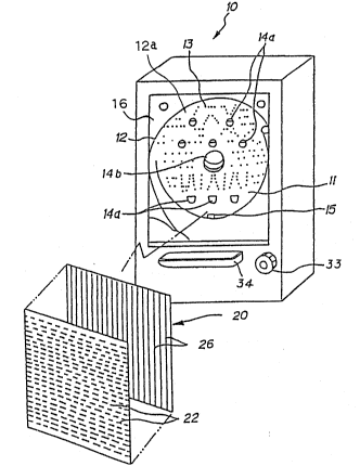
The pinball machine shown in Figure 3 has a base board 11
for providing a space required to move pinballs, a surface glass ~`
substance 16 spaced from the base board 11 at 'a given interval to
cover the base board, and a propelling mechanism for propelling
S pinballs in the space provided by the base board 11 and the
surface glass substance 16. The pinball machine is set up so that
the base board 11 becomes substantially parallel to the vertical
direction .
The base board 11 is provided with a guide rail 12. The
1 Q inner area of the base board 11 surrounded by the guide rail 12
provides a gaming area 12a. The guide rail 12 guides a pinball
propelled by the propelling mechanism along the rail to the upper
position (upstream part) in the vertical direction of the gaming ~ ,
area 1 2a.
The gaming area 12a is formed with a plurality of safe holes
14a for the player to enter a pinball in for a winning game play :
through which the pinball is discharged from the base board 11, a
winning game play effect device 14b being located at the center of
the base board from upstream to downstream for providing a
special winning game play condition, and an out hole 15 into -- -
which pinballs not entered in the safe holes 1 4a are finally - -
collected for discharging the pinballs from the base board 11. ~ ~ -
The winning game play effect device 14b is a device whose;~
state changes each time a pinball enters a specific safe hole 14a, -
which pays out a large number of pinballs to the player far a `
winning game play when a certain condition is satisfied. For
. ~`' ',.
2~ 1 ~3 03
1 4 ~~:
example, rotating drums as with a slot machine~ are provided and
each time the player wins a game play, are rotated. When a
predetermined symbol pattern is complete, a lalrge number of
pinballs are paid out to the player for a special winning game
play. ;1;- ~-~
The gaming area 1 2a of the base board 11 is provided with a
large number of pins (nails) 13 with which pinballs B dropping
along the base board 11 frequently collide for causing their
motion direction to fluctuate. The pins 13 are hammered into the
1 0 base board 11 substantially vertical to the base board 11 in a
state in which they project from the base board 11 as long as the
diameter of the metal substance B, as shown in Figure 4. The pins
13 are distributed on the base board 11 for the purposes as
described above.
A propelling handle 33 for players to propel pinballs and a
pinball return 34 for receiving pinballs paid out for winning game
plays are located on the front face of the pinball machine 10. The : -
handle 33 is a part of the propelling mechanism.
As shown in Figure 4, front glass covering the base board 11
2 0 has a double structure consisting of the surface g}ass substance 16
and an inner glass substance 1 7 along the base board 11 of the
pinball machine 10. The inner glass substance 17 consists of a
glass substrate 17a and surface glass 17b and 17c bonded to both
faces of the glass substrate 17a. ;
~` '"'" `;
. . : ~. ~
. - . , -
. .
Next, a fir~t er~ibodLlT~t of a metal su~stance detection syst~n
of the invention will be discussed with reference to the
accompanying drawings.
The metal substance detection system of the embodiment
5 comprises a matrix sensor 20 having a de~ection area spreading
like a plane and ~unctioning as a meta} sensor and a signal
processing system ~signal processing apparatus) 170 which drives
the matrix sensor 20 for sensing the presence of a metal substance
and detecting the position thereof, as shown in Figure 6.
The matrix sensor 20 has a plurality of transmission lines ~- ~
22, a plurality of reception lines 26, and a board for supporting ~` -
the lines, as shown in Figure 5. Each of the transmission lines 22 ---
consists of a pair of conductors 62 forming a going way 62a and a
returning way 62b which are parallel. Likewise, each of the
15 reception lines 26 eonsists of a pair of conductors 62. In the
embodiment, the conductor 62 is made of copper wire coated with --
polyurethane for insulation, for example. A pair of the conductors
62 comprises a going way and a returning way connected on one - `
end and serving as input and output terminals of a signal on the
2 0 other end.
The transmission lines 22 and the reception lines 26 are ;~
placed so as to cross each other. Specifically, ~or example, the
transmission lines 22 are arranged at given intervals in a row ; . -
direction and the reception lines 26 are arranged at given
25 interYals in a column direction. The transmission lines 22 and the
reception lines 26 are placed in such a manner to provide the
~:. ': '" " '`'`
~ ~ . .. :
:
2 1 ~ ~ ~ 0 3
1 6 -
, .: . - . --
intersections of the transmission lines 22 and the reception lines
26 like a matrix as sensing regions. Either the transmission lines
22 or the reception lines 26 may be placed in the row or column -
direction as desired.
The signal processing system 170 has a ;
transmission/reception board 171 functioning as
transmission/reception means for driving the matrix sensor 20
.
and a control board 172 functioning as signal processing means for
controlling the transmission/reception board 171 for receiving a
detection signal and determining whether or not a metal
substance exists based on the detection signal and detecting the
metal substance sensing position when a metal substance exists. ~- The transmission/reception board 171 has a transmission
~, .' ' ., . ' 1 :'
circuit 40 (see Figure 7) for scanning the specified lines of the
transmission lines 22 in sequence and sending a transmission
signal thereto and a reception circuit 50 (see ~igure 9) for
scanning the specified lines of the reception lines 26 in sequence
and reading reception signals of the reception lines in sequence, as
described below. The control board 172 specifies the transmission
2 0 and reception lines to be scanned for the transmissionlreception
board 171, determines whether or not a metal substance exists
from a signal received at the reception circuit 50, and detects the ~ ~:
metal substance sensing posieion based on information indicating
the transmission line scanning position at the transmission circuit
2 5 40 and information indicating the reception line scanning position
at the reception circuit 50.
..
..~
~ :- . . . ..
2~83~3
1 7
The control board 172 can store information indicating the
presence position of a pinball in time sequence for finding the
move path of the pinball. From the move path, the characteristics ~-
of the pinball machine can be known and an abnormal path can --
S also be detected for judging whether or not illegal operation has
been performed.
Next, the matrix sensor will be described in more detail. - -
As shown in Figure 4, the matrix sensor 20 is formed like a
plane within the inner glass substance 17, which is on the side of
1 0 the base board 11, of the two glass substances covering the base
, -: ...:
board 11, and therefore is disposed between the front glass
substance 16 and the base board 1 1.
As shown in Figure 5, in the matrix sensor 20, the
transmission lines 22 are placed on one face (on the side of the --
surface glass,~ of the glass substrate 17a of the inner glass - `
substance 17 in parallel in one direction. F,ach transmission line ~ -
22 is located on the glass substrate 17a so as to make a U-turn ~
(parallel turn form) at the end of the glass substrate 17a. -
Likewise, the reception lines 26 are placed on the opposed
20 face (on the side of the base board 11) of the glass substrate 17a
of the inner glass substance 17 in parallel in one direction. Each
reception line 26 is located on the glass substrate 17a so as to
make a U-turn (parallel turn form) at the end of the glass ~ ~ -
substrate 17a. A ~ransmission terminal section 23 and a reception
25 terminal section 27 functioning as connection sections of the
transmission lines 22 and the reception lines 26 are placed
'"' '. " "'',, ' . ' ' ' ' ~ ~ , ' ~ . ' ' '`
21~8~3 ~ :
18
collectively on the lower end of the inner glass substance 17 in top
and bottom relation when the matrix sensor is mounted on a -
pinball machine.
The reception lines 26 are located at right angles to plane
S parallel positions with the transmission lines 22 so as to be
electro-magnetically coupled with the transmission lines 22,
namely, in positional relation such that a magnetic flux from the
transmission line 22 interlinks. The transmission lines 22 and the
reception lines 26 with the inner glass substance 17 as a substrate
1 0 make up the plane matrix sensor 20.
As shown in Figure 5, square portions surrounded by the ~ ~
transmission lines 22 and the reception lines 26 crossing each - ~ ~-
other, detection positions, provide sensing units 20a, 20a, ... for
sensing a metal substance. In the embodiment, the sensing unit ~ -~
1 5 20a, 20a, is set to a size being capable of sensing a pinball.
The inner glass substance 17 is a glass substrate of a
quadrangle having dimensions of 367 mm +10 mm in length a and
367 mm ~10 mm in width b and 3.0-3.5 mm in thickness. ~ach of - -
the surface glass 17b and 17c is shorter than the glass substrate
17a in length and the lower end of the glass substrate 17a is
exposed. ` To form the inner glass substance 17, the transmission lines
22 are bonded to one face of the glass substrate 17a with a
transparent adhesive layer and the surface glass 17c is bonded
thereon with a transparent adhesive layer; the reception lines 26 ~ - -
are bonded to the other face of the glass substrate 17a with a `
2~8303 ~ :-
9 '
,. ' ~ '
transparent adhesive layer and the surface glass 17b is bonded --;
thereon with a transparent adhesive layer. As shown in Figure 5,
a turn substrate 19a and a transmission route substrate l9b like -
an L letter are disposed in the left end part andl right end part,
S respectively, on one face. ~ ~-
A turn substrate 29a and a route substrate 29b are disposed
in the upper end part and lower end part, respectively, on the
other face of the glass substrate 17a. `
As shown in Figure 5, each of the transmission lines 22
1 0 consists of a turn part 61 formed on the turn substrate l9a and
wires 62a and 62b soldered to the turn part 61. The input and
output terminals of the transmission line 22 are connected via - ~
route wire to the transmission terminal section 23.
On the other hand, as shown in Figure 5, each o~ the ; - ~.
1 5 reception lines 26 consists of a turn part 61 formed on the turn
substrate 29a and wires 62a and 62b soldered to the turn part 61.
The lower end part of the reception line 26 is connected to the
reception terminal section 27 by a route part 64 formed on the
route substrate 29b bonded to the lower end of the other face of
2 0 the glass substrate 17a.
To make the wires 62a and 62b inv~isible for the customers,
their surfaces are of a matte black finish intended for protecting
against light reflection.
A preferred pattern of the matrix sensor 20 of a normal
pinball machine 10 consists of 32 rows of the transmission lines ~ - .`;~22 and 32 columns of the reception lines 26, namely, 1024 sensing
2 1 1 g 3 ~ 3
2 0
units 20a in total. The embodiment takes the pattern of the 32
rows of the transmission lines 22 and 32 columns of the reception
lines 26 as an example. In Figure S, only outer parts of the
pattern are shown.
S Preferably, each of the wires making up the transmission
lines 22 and the reception lines 26 is 25,um 3011m thick. In the
embodiment, as shown in Figure 5, the whole widths of the
transmission terminal section 23 and the reception terminal
section 27, c and d, are each 126 mm and the widths of the
1 0 longitudinally extending portions of the transmission turn
substrate 19a and the transmission route substrate 19b, e and f,
are formed each 10 mm or less. The width of one line of the -
transmission terminal section 23 and the reception terminal
section 27 is 1.5 mm.
1 5 The matrix sensor 20 is formed with a connector mounting
plate 66 in the lower end part of the glass substrate 17a. The
connector mounting plate 66 has both sides between which the
lower end of the glass substrate 17a is sandwiched, and is integral
with the inner glass substance 17. The connector mounting plate
66, which is made of plastic or stainless material, extends
downward along the width of the inner glass substance 17 and is
on an extension plane of the inner glass substance 17 of the
matrix sensor 20.
A transmission connector 67a and a reception connector 67b ;~ -
are fixed to the positions of the connector mounting platei 66
colTesponding to the transmission terminal section 23 and the
2113303 ~ ~ ~
2 1
reception terminal section 27. The terminals of the transmission
terminal section 23 and the reception terminal section 27 are
connected via these connectors to the transmission circuit 40 and :
the reception circuit 50.
The connector mounting plate 66 has the thickest portions in :
which the transmission connector 67a and the reception connector
67b are mounted. Qn the other hand, the transmission connector
67a and the reception connector 67b are short and the thickest
portion of the connector mounting plate 66 is as thick as or
1 0 slightly thinner than the inner glass substance 17 of the matrix
sensor 20.
The transmission/reception board 171 (see Figure 6)
connected to the transmission connector 67a and the reception ~`
connector 67b is placed on the connector mounting plate 66. The
1 5 transmission/reception board 171 has the transmission circuit 40
(see Figure 7) for transmitting signals to the transmission lines 22
of the matrix sensor 20, the reception circuit 50 (see Figure 9) for
receiving signals from the reception lines 26, and junction
connectors (not shown) connected to the transmission connector
2 0 67a and the reception connector 67b.
The junc~ion connectors are connected to the transmission
connector 67a and the reception connector 67b for connecting the
transmission terminal section 23 to the transmission CiTCUit 40
and the reception terminal section 27 to the reception circuit 50.
2 5 Next, the signal processing system which processes signals of : - :
the matrix sensor 20 will be described.
21~303
2 2
"'
As shown in Figure 6, the matrix sensor 20 is placed under
the control of the control board 172 spaced from the matrix sensor
20 via the transmission/reception board 171. The control board
172 has an information processor 30 shown in Figure 10 and can
5 communicate with other systems on a communication line 179.
The control board 172 also has an interface section 176 for the
information processor 30 to read moni~or points from a card 173. - ~
The information processor 30 has at least a central processing unit -
(CPU) (not shown) and a memory (not shown) for storing CPU ~ -
1 0 programs and data.
The card 173 is a memory card that can be mounted and
demounted on the interface section 176. The card 173 stores at
least data indicating pinball monitor points such as detection
positions of pinballs propelled into safe holes 14a, 14a, ... and a
lS game area provided on the base board 11 of a pinball machine 10,
and the position of an out hole 15; and a detection algorithm of
pinballs entering the safe holes 14a, 14a, ... and the out hole 15, as
monitor data. In the embodiment, the card 173 further stores
scan information specifying the transmission and reception lines -
2 0 to be scanned.
The memory mounted on the card can use RAM, mask ROM, ;
EPROM, one-shot ROM, etc.
A storage 174 connected to the control board 172 is used to
record paths of pinballs moving in space between the base board
2 5 11 of the pinball machine 10 and the inner glass substance 17.
The storage 174 can be provided by a hard disk storage device, ~ -
~: ~
2~1~3~3
2 3
... .. ,, ~- ~.
for example. The data recorded in the storage ]l74 can be loaded ~; -
into a computer 175 containing software for analyzing pinball ~-
paths and performing operations on the data to provide data -
required for the pinball parlor. All or a part of the data indicating
5 the monitor points, the pinball detection algoriehm, and scan
:.-- ~ .: .,- .
information may be stored in the storage 174. ` `~
....... -- . .~
The transmission CilCUit 40 is a circuit for transmitting a
signal of a predetermined frequency to each transmission line 22 ~ ~ ~
in sequence. The reception circuit 50 is a circuit for receiving a ; -
signal from each reception line 26 in sequence in synchronization
with the transmission circuit 40. A continuous sine wave of
frequency 1-1.3 MHz centering on 0 V is preferred as a voltage
waveform applied to the transmission line 22 by the lransmission
circuit 40.
As shown in Figure 7, the transmission circuit 40 consists of
a transmission connector 41, an amplifier 42 connected to the
transmission connector 41, a transmission line switch circuit 43a ~ ~ -
for switching the transmission line to which a signal current is to -
be transmitted in sequence each time a transmission line switch ~
. .
2 0 pulse is input, and 32 totem-pole drivers 45 each connected to one
end of each of ehe 32 transmission lines 22 via the transmission
connector 67a. The transmission line switch circuit 43a has a
channel switch logic 43 and an analog multiplexer 44 being ~-
connected to the amplifier 42 and the channel switch logic 43 for
2 5 swi~ching so as to connect the amplifier 42 to the totem-pole --
driver 45 corresponding to the specified transmission line 22. -
..:
.
~ .
2 1 ~ ~ 3 ~ 3
2 4
Each totem-pole driver 45 comprises an NPN tr,ansistor and a PNP --;
transistor, which have emitters connected to each other and bases
,. ".
connected to each other.
The channel switch logic 43 has a counter IC 43a and ~ --
5 operates with two control lines for clock and reset, as shown in
Figure 8. Specifically, each time a transmission line switch pulse is
input from a transmission line switch pulse generating circuit 204
of a sequence controlling circuit 47 described below, the
connection state of the analog multiplexer 44 is switched in
1 0 sequence so as to connect to the specified transmissiorl line.
As shown in Figure 9, the reception circuit 50 consists of 32
CTs (current transformers) 51 connected to the 32 reception lines
26 via the reception connector 67b, a reception line switch circuit
54a being connected to the CTs 51 for switching the reception line
1 5 to be detected in sequence each time a reception line switch pulse ~ ~ ;
is input, an amplifier 53 connected to the reception line switch
circuit 54a, and a reception connector 55 connected to the ;
amplifier 53 and the reception line switch circuit 54a. The
reception line swi~ch circuit 54a has an analog multiplexer 52 and
2 0 a channel switch logic 54 connected to the analog multiplexer 52.
Therefore, the reception circuit 50 is adapted to receive a signal
from each reception line 26 via each CT 51.
The CT 51 insulates its corresponding reception line from the
analog multiplexer 52 and magnifies a signal from the
2 5 corresponding reception line by 10 times. The analog multiplexer
52 receives signals in sequence from the specified CTs 51 based on
,, . ~
,
':
. . ~ . .
'~ ' ~ . '
:' ' ,. ': " , ' ' '
2 1 ~ 3
2 5 :~
a command of the channel switch logic 54. The amplifier 53
amplifies a signal from the analog multiplexer .52. -~
The channel switch logic 54 is similar element to the channel -~
switch logic 43 of the transmission circuit 40. Each time a
5 reception line switch pulse is input from a reception line switch
pulse generating circuit 202 ~described below) of the sequence ~; -
controlling circuit 47 (every scanning period), the input switch :
state of the analog multiplexer 52 is changed on the falling edge of
the pulse signal. :
As shown in Figure 10, the control board 172, which ~:~
contains the information processor 30, has a transmission section
comprising a sequence controlling circuit 47 for sending a
transmission clock in response to a start signal input from the .
information processor 30 via a CPU connector 46, a band-pass -~15 filter 48 for receiving the transmission clock and outputting a
transmission signal, and an amplifier 49 for amplifying the
transmission signal and sending the amplified signal to the . : :.
transmission connector 41.
The control board 172 has a reception section comprising an
2 0 amplifier 71 for amplifying a reception signal from the reception
connector 55, a band-pass filter 72 for receiving the amplified
signal, a full-wave rectification amplifier 73 for receiving the
reception signal through the band-pass filter 72, two low-pass
filters 74a and 74b for receiving the reception signal from the --~2 5 full-wave rectification amplifier 73, an A/D converter 75 for
receiving the reception signal through the low-pass filter 74b,
` ~ ``~ `` `
: ` . ~
''"',:`,' '' ' ' , : ' ' `' ' ' , ' ' .
2 1 ~ ~ 3 0 3
2 6
',-,;~ .'',", ,',`~
" .': """~ -;
converting the reception signal into digital data under the control
of the sequence controlling circuit 47, and outputting the digital
data, and a dual port RAM 76 for writing the d:igital data under
the control of the sequence controlling circuit 4'7 and sending the
data via the CPU connector 46 to the information processor 30 in :~
response to a read signal from the CPU connector 46. . ~:
The control board 172 has a power unit 77. The ~:
dual port RAM 76 has a capacity of 2048 bytes, for example.
The sequence controlling circuit 47 has a function of :
outputting a basic clock used as a source of a signal input to each
transmission line 22 and a function of outputting the above~
mentioned reception line switch pulse signal (first timing signal)
for controlling the channel switch logic 54 and the above-
mentioned transmission line switch pulse signal (second timing
signal) for controlling the channel switch logic 43.
That is, the sequence controlling circuit 47 comprises a clock
circuit 201 for outputting a basic clock signal, a reception line
switch pulse generating circuit 202 for dividing the basic clock ;
*om the clock circuit 201 for outputting a reception line switch -
pulse signal (RXCLK in Figure 2) every scanning period, for
example, every basic clock, an interrupt pulse signal generating
circuit 203 for further dividing the output of the reception line - ~-
switch pulse generating circuit 202 for forming two pulses each
time all reception lines 26 are switched (each time 32 reception ~ :
2 5 line switch pulses are output) and generating two interrupt pulses ~ -
(INT in Figure 2) on the rising edges of the two pulse signals, and
27
a transmission line switch pulse generating circuit 204 for
outputting as many transmission line switch pulse signals (TXCLK - -~
in Figure 2; each having extremely short pulse width as compared
with the reception line switch pulse signal) as the skip count
S specified by the information processor 30 on the rising edge of
every other interrupt pulse signal.
The sequence controlling circuit 47 has a circuit (not shown)
for di~iding the basic clock for outputting the transmission clock. ~ ~
In the detection operation, the information processor 30 ;
reads the aboYe-mentioned scan information from the card 173
(storage medium), receives the interrupt pulse signal lNT from the
interrupt pulse signal ~enerating circuit 203, and sets a new skip
count in the transmission line switch pulse generating circuit 204
each time all reception lines 26 are switched. That is, if the next -
transmission line ready to transmit an input signal does not
receive transmission specification in the course of switching a ~ `
sequence of the reception lines, in the embodiment, at the timing
of switching to the 17th reception line or on the rising edge of the
interrupt pulse signal INT as shown in Figure 2, the information
2 0 processor 30 instructs the transmission line switch pulse
generating circuit 204 to skip the transmission line. lf continuous
transmission lines are not used for signal detection, the
information processor 30 instructs the transmission line switch
pulse generating circuit 204 to skip these transmission lines.
2 5 The transmission line switch pulse generating circuit 204
outputs the transmission line switch pulse signal TXCLK in the
~ ~ . . . . . . ... ..
28
f -
interrupt pulse period next to the skip setting (in Figure 2, at the
timing of switching to the first reception line). At the time, if the
next transmission line is not skipped, one pulse is output, thereby ~;
switching the current transmission line to the next transmission
5 line. However, if the next transmission line is to be skipped,
successively the transmission line switch pulse signal TXCLK iS
output, thereby switching the current transmission line to the next
next transmission line; the next transmission line on whicll a
transmission signal should be transmitted is skipped. Therefore,
10 the transmission line switch pulse generating circuit 204 outputs
one pulse of the transmission line switch pulse signal TXCLK for
switching the current transmission line to the next transmission -
line or (n+1) pulses of the transmission line switch pulse signal ;
TXCLK for skipping one or more successive signal lines, where n is
15 the number of signal lines to be skipped.
The information processor 30 is also programmed so
as to read monitor area data registered on the card 173 and sense
data stored in the dual port RAM 76, and compare the sense data
with the monitor area data of pinballs for monitoring pinballs,
20 independently of the detection operation under the control of the
sequence controlling circuit 47 or the information processor 30.
Next, the operation of tlle embodiment will be described.
Address signals and control signals from the information
processor 30 are output via the CPU connector 46. Figure 11 ~ -
25 shows a process flow. First, an example in which scanning of all
transmission lines is specified will be discussed. ; ~;
~ , - ... . .
1, :- . ~ , , .
21 ~3~3
2 9
When a start signal is transmitted from the information
processor 30 to the sequence controlling circuit 47, the sequence : : .
controlling circuit 47 divides a 1 6-MHz basic clock in response to . -
necessary clock frequency for generating and outputting a
S transmission clock. The waveform of the transnnission clock from
the sequence controlling circuit 47 is shaped from digital signal .
into analog signal through the band-pass filter 48, then the analog ;.
signal is amplified by the amplifier 49 and sent to the
transmission connector 41.
Further, the transmission signal is amplified by the amplifier ::
,
42 in the transmission circuit 40. The analog multiplexer 44
operates the totem-pole drivers 45 in sequence on channels .
switched by the channel switch logic 43, whereby the totem-pole --.
drivers 45 output the signal amplified by the amplifier 42 to the :~
15 transmission lines in sequence (step 9 1 ).
Then, electromagnetic induction effect causes an
electromotive force to occur on the reception lines 26 crossing the
transmission line 22 on which the signal is transmitted. At the
time, as a pinball which is metal approaches a sensing unit 20a,
2 0 the magnitude of the electromotive force (induced current) of the
reception line 26 changes in the sensing unit 20a. -~
The reason why it changes is not analyzed clearly at present,
but can be considered as follows: First, a pinball, which made of a
material consisting essentially of iron, is a ferromagnetic
2 5 substance. Thus, a magnetic flux occurring on the transmission
line 22 and spread ints) a space converges on the pinball and the
2~ 830~ :
. ~;.'
magnet;c flux distribution interlinking the reception lines changes.
At the same time, an eddy current occurs on the pinball in a
direction of canceling the magnetic flux on the transmission line
22. These cau~ies the induced current to change. Which cause is
5 dominant varies depending on ~he relative positional relationship
between the pinball and the transmission line 22 and reception
line 26. Whether or not the magnetic flux interlinking with the
reception line 26 increases also varies depending on the relative
positional relationship with the pinball. It also varies depending
on whether or not metal exists on the background. ; -
In the reception section, the reception circuit 50 receives a
signal from each reception line 26 via each CT 51 in
synchronization with the transmission circuit 40 under the control
.
of the sequenee controlling circuit 47. As shown in Figure 9,
voltage caused by induced current appearing on the reception ~--
lines 26 is magnified by 10 times by the CT 51. To convert the
voltage by the CT 51 eliminates the need for making a large
amplification degree of the amplifier in the reception circuit. The
CTs 51 insulate the reception lines 26 of the matrix sensor 20
2 0 from the analog multiplexer 52 in the reception circuit 50 for
preventing noise from entering the reception circuit 50 from the
pinball machine 10.
The analog multiplexer 52 switches signals received from
the reception lines 26 through the CTs 51 by the channel switch
25 logic 54 and outputs ~hem in sequence. Each signal output from
'' '~ ''
.~, -.. , . - . , -
2 ~ 3
31
the analog multiplexer 52 is amplified by 100 times by the
amplifier 53 (s~ep 92).
The reception signal is amplified and detected via the ~;
reception connector 55, the amplifier 71, and the band-pass filter ~;
5 72. The recep~ion signal passed through the band-pass filter 72
results in an analog signal, which is then shaped by the full-wave
rectification amplifier 73. The output signal from the full-wave
rectification amplifier 73 is averaged by integration processing
through the low-pass filters 74a and 74b.
1 0 Next, the reception signal is sent to the A/D converter 75.
The A/D converter 75 converts the signal from the reception linc
26 into a digital signal in predetermined bit units, such as 12 bits,
and outputs the resultant digital signa} (sense data) to the dual
port RAM 76 for storage under the control of the sequence ; ~
1 5 controlling circuit 47 (step 93). ~ -
That is, the sense data is recorded in the dual port RAM 76
in response to a write signal from the sequence controlling circuit
47 independently of the operation of the information processor
30, then the address is incremented by one every scanning period
2 0 based on the clock signal output by the sequence controlling ~ -
circuit 47, for example, every clock (step 94), and the sense data is
stored in a different address for each sensing unit 20a. -
These steps are repeated every scanning period. That is, the
analog multiplexer 52 in the reception circuit 50 switches the
2 5 signal from each reception line 26 every scanning period at step
95 and the above-mentioned operation is performed 32 times for ;
~.. .. . . .
21~8~
32
' ~ ~
ehe 32 reception lines 26 (one for each line) at step 96. Upon
completion at step 96, the analog multiplexer 44 in the
transmission circuit 40 switches ~he current transmission line 22
at step 97. Again, similar processing is repeated 32 times for
storing the sense data for each sensing unit 20a in different
addresses of the dual port RAM 76 in sequence in rela~ion to the
sensing units 20a. ~ `
Therefore, the information processor 30 can read the sense
data stored in the dual port RAM 76 for judging a pinball exists at
what time at what position ~sensing unit 20a) under any desired
retrieval conditions whenever necessary independently of the
above-mentioned detection signal processing.
Thus, the information processor 30 can read the sense data ;;
recorded in the dual port RAM 76 by a read start signal, as
required, perform operations on the read sense data, and compare
the sense data with the pinball monitor data stored on the card
173 for monitoring pinballs.
The oper~tion is repeated every scanning period.
Next, an example in which a transmission signal is not sent
2 0 to some of the transmission lines 22 will be discussed. -
Not to send a transmission signal, information indicating
lines to which no transmission signal is sent, namely, lines not to
be scanned, needs to be specified. The specification may be either
specification of lines not to be scanned or of lines to be scanned.
2 5 In the embodiment, the card 173 provides the signal processing
21~303
33
system with scan information specifying the transmission lines 22 ~ -~
to be scanned.
The information lines 22 for which detection is not specified -
in the scan information provided by the card 173 are skipped by ~.
the operation of the scanning system described above. The reason
why the card 173 provides the signal processing system with the
scan information is that even if the configuration of the pinball
machine is changed, the signal processing system can deal with
the change without modification of the system. :
The channel switch logic 54 and the analog multiplexer 52
switch a signal from each reception line 26 in sequence every
scanning period indicated by the reception line switch pulse signal ;
RXCLK (see step 95). Upon completion of 32 repetitions of the
operation for the 32 reception lines 26 (see step 96), the channel
switch logic 43 and the analog multiplexer 44 switch the current
transmission line 22 based on the transmission line switch pulse ;
signal TXCLK (see step 97). Again, similar processing is repeated
32 times. The number of pulses of the transmission line switch
pulse signal TXCLK output when the transmission line is switched
is the skip count set in the transmission line switch pulse
generating circuit 204 by ~he information processor 30 on the
rising edge of the interrupt pulse signal preceding the current -
interrupt pulse signal, as shown in Figure 2. Therefore, as many
transmission lines 22 as the skip count are skipped. ~ ~
2 5 For example, when the next and next next transmission lines i ~ -
22 to which a signal is to be input are not registered as detection ~ ~
.,'`. ~ .~.
`
2i~83~
3 ~
positions in the scan information registered on the card 173, three
pulses of the transmission line switch pulse signal TXCLK are
output as shown in Figu}e 2. Thus, the two transmission lines 22
are skipped. ~ -;
The transmission line switch pulse signal TXCLK is shown in
magnified wavelength in Figure 2; in fact, it has an extremely
short pulse width. The skip operation is performed for
considerably shorter time than the scanning period. Thus, the
.,; ~
skip time does not hinder the detection operation on the first ~`` `
reception line 26 immediately after the transmission line is
switched.
The information processor 30 can Tead the sense data stored ~ ;
in the dual port RAM 76 for judging a pinball exists at what time ;
at what position (sensing unit 20a) under any desired retrieval
conditions whenever necessary independently of the above~
mentioned detection signal processing. -
Thus, the information processor 30 can read the sense data
recorded in the dual port RAM 76 by a read start signal, as
required, perform operations on the read sense data, and compare ~ `~
2 0 the sense data with the pinball monitor data stored on the card
173 for monitoring pinballs.
The metal substance detection system of the embodiment
can omit the detection operation on specific transmission lines as
specified in the scan information stored on the card 173 that can
2 5 be set as desired by the user and perform the detection operation ~;
; '-::.
':''.. '
only on the specified transmission lines 22 one after another;
pinballs can be managed based 011 the delection operation results.
Therefore, if the metal substance detection system is used ~ ~ ;
for detecting pinballs, the scan informat;on can be set according to
the pinball machine type, etc., for scanning a minimum necessary
range corresponding to the pinball machine type, etc., witllout
wasting the time for improving the detection speed.
In the embodiment, the sequence controlling circu.it 47
outputs a first timing signal to the reception circu~t 50 for
scanning the lines in sequence and a second timing signal to
the tran~mission circuit 4a for switching the current scanning
to the next line each time all reception lines have been
~aanrled. Therefore, lines not to be scanned are specified for
the tran~mission lines ~canned in response to the second -~
timing signal. ~owever, the invention is not limited to the
configuration. For example, all transmis~ion lines may be :~
ecanned and some reception lines may be skipped, in which case
replacement may be made in the circuit shown in Figure 1 80
that the output of the reception line switch pulse generating
c~rcuit 202 ~hould be se~t to the channel ~witch logic 43 and
the output of the transmis~ion line switch pulse generating
oircuit 204 should be sent to the channe~ switch logic 54.
Next, a second embodiment of the invention will be ~ ~
discussed with reference to the ~ccon~panying drawings. - ; -
The second embodiment comprises a matrix sensor 20 and a
signal processing system 170 which drives the matTix sensor 20,
as shown in Figure 14. -
As shown in Figure 13, the matrix sensor 20 has
transmission lines 22 and reception lines 26, each line consisting
' :' ~' `; "': -
2i 1 8303 ~
36
. ~
of a pair of conductors 62, placed on a board 17 so as to cross each ~ -
other, as in the first embodiment. The second embodiment differs
from the first embodiment in that the transmission lines 22 and
the reception lines 26 do not make up a complelte matrix. That is,
5 three transmission lines 22 are disposed at positions
corresponding to safe holes 14a and three reception lines 26 are
disposed at positions corresponding to safe holes 14a, as shown in
Figure 12.
Position data of the safe holes 14a, 14a, ... made on a base
10 board 11 of a pinball machine 10, a detection algorithm of pinballs
entering the safe holes 14a, 14a, ..., or the like are recorded on a
card 173 as monitor data, as in the first embodiment.
As shown in Figure 15, a transmission circuit 40 consists of a
transmission connector 41, an amplifier 42 and a channel switch
1 5 logic 43 connected to the transmission connector 41, an analog
multiplexer 44 connected to the amplifier 42 and the channel
switch logic 43, and three totem-pole drivers 45 connected to the
analog multiplexer 44 and also connected to three transmission
lines 22 via a transmission connector 67a.
As shown in Figure 16, the reception circuit 50 consists of a -~
plurality of, concretely three CTs 51 connected to three reception
lines 26 via a reception connector 67b, an analog multiplexer 52
connected to the CTs 51, an amplifier 53 and a channel switch
logic 54 connected to the analog multiplexer 52, and a reception
connector 55 connected to the amplifier 53 and the channel switch
;. . .
- ' ~ :-. - - ,-,
'` ~.' ,~ `,..''~ '
. ~: ... -.
21l830~ : ~
- -: -
37
logic S4. Therefore, the reception circuit 50 is adapted to receive
a signal from each reception line 26 via each CT 51.
The operation of the second embodiment is basically the ~ ~;
same as that of the first embodiment in which no skip is executed,
except that the loop is broken when three repetitions are made at
step 96 in Figure 11. That is, when the analog multiplexer 52 in
the reception circuit 50 switches a signal from each reception line
26 every scanning period and completes the operation three times
for the three reception lines 26, the analog multiplexer 44 in the -
transmission circuit 40 switches the current transmission line 22.
Similar processing is repeated three times and sense data about
sensing units 20a is registered in different addresses of a dual -~
port RAM 76 in sequence in relation to the sensing units 20a. ; ~ ~
Therefore, the information processor 30 can read the sense ~ "
data stored in the dual port RAM 76 for judging a pinball exists at ~ -
what time at what position (sensing unit 20a) under any desired
retrieval conditions whenever necessary independently of the
above-mentioned detection signal processing. -
Thus, the information processor 30 can read the sense data
2Q recorded in the dual port RAM 76 by a read start signal, as
required, perform operations on the read sense data, and compare
the sense data with the pinball monitor data stored on the card
. ~
173 for monitoring pinballs.
In the pinball detection system, the transmission lines 22
2 5 and the reception lines 26 are ~isposed corresponding to the safe
holes 1 4a on the base board 11 so that their intersections 20a
`'`'`'`':'','```~
, . . . . . . , .. .. - . .. . .. ...... - , . ; . . . . .
~118~3 ~i-
38
become positions of the safe holes 1 4a, thus the number of the
transmission lines 22 and the reception lines 26 to be scanned
becomes ~he minimum number corresponding to the safe holes (in
the example, each three lines), and the detection speed can be
improved drastically while the important detection range is ~ ~ ~
maintained . . ~ -
The locations and ~orms of the transmission and reception
lines in the invention are not limited to those in the embodiments;
for example, a pair of transmission and reception lines 22 and 26
may be provided paying attention to only one safe hole 14a, as
shown in Figure 17.
Next, a third embodiment of the invention will be discussed
with reference to the accompanying drawings.
The third embodiment has a matrix sensor 20 and a signal
processing system 170 which drives the matrix sensor 20, as
shown in Figure 6.
The third embodiment di~fers from the first embodiment in . ~::
that it is provided with a data converter section 400 at the stage .
preceding an information processor 30 in the signal processing .
20 system 170. The data converter section 400 compares a reception
signal from each reception line 26 with reference data for
converting the signal into response data (difference data)
representing a change in an induced current on the reception line
26 for decision in the information processor. Other configuration : ~ -
2 5 of the third embodiment is as the same as that of the first
embodiment. The third embodiment can be applied to both a case
~';: ;'`````''`'`
2 ~ ~g 3 ~ 3 ~: ~
3 9
where transmission lines 22 are not skipped and a case where
transmission lines are skipped in the first embodiment. It can
also be applied to the second embodiment. .
The signal processing system 170 has a
S transmission/reception board 171 and a control board 172, as
shown in Figure 6.
The control board 172 has an information processor 30, as ~ ~:
shown in Figure 18. The control board 172 has a transmission -:
section comprising a sequence controlling circuit 47 for sending a
1 0 transmission clock in response to a start signal input from the ::
lnformation processor 30 via a CPU connector 46t a band-pass
filter 4~ for receiving the transmission clock and outputting a :
transmission signal, and an amplifier 49 for amplifying the :
transmission signal and sending the amplified signal to a
1 S transmission connector 41.
The control board 172 has a reception section comprising an
amplifier 71 for amplifying a reception signal from the reception .
connector 55, a band-pass filter 72 for receiving the amplified
signal, a full-wave rectification amplifier 73 for receiving the
2 0 reception signal through the band-pass filter 72, ~wo low-pass : . - -
filters 74a and 74b for receiving the reception signal from the
full-wave rectification amplîfier 73, an A/D converter 75 for
receiving the reception signal through the low-pass filter 74b,
converting the reception signal into digital data under the control
2 5 of the sequence controlling circuit 47, and outputting the digital
data, data converter section 400 for receiving the digital data as
. ~.
: . . .
-~,~'- : ' " ' ' . - '
4 0
" ~
raw data X and converting the raw data X into response data Z ~ `; ;
representing the presence or absence of an electro-magnetic
characteristic change at each sensing position (presence or absence
of a pinball), and a dual port RAM 76 for writing the response ~ m -
data Z under the control of the sequence controlling circuit 47 and ;
sending the response data Z via the CPU connector 46 to Ille
information processor 30 in response to a read signal from the - -
CPU connector 46.
As shown in Figure 19, the data converter section 400
comprises a data latch circuit 401, a data switch circuit 402, a
comparator 403, an opcrational circuit 404, an operation result
latch circuit 405, a re~erence memory 406, an address generating
circuit 407, a RAM address switch circuit 408, a CPU access switch
circuit 409, and a controlling circuit 410. The circuitry containing ~-
the memory can be provided by a one-chip IC. The data converter - ~
section 400 operates each time data about one sensing unit is ~ ;
obtained. At the time, the -;
daea converter section 400 has the two operation modes: The first
is a mode of making a calculation from expression (1) described
below and the second is a mode of making a calculation from
expression (2) described below.
The data latch circuit 401 inputs an output of the A/D ~ c
converter 75 on a scanning period of reception line 26 of the
matrix sensor 20, for example, 28 ~,lsec, and holds it until the next
~2 5 sampling period. In the description to follow, the data input by
the data latch circuit 401 is represented as raw data X for -
."
. . - ~: - , :
~- ~ . , .
.: - .
:::
4 1
,: ~
convenience. There are as many pieces of raw data X as the ` . ~ -
number of sensing units 20a of the matrix sensor 20, for example,
1024
The data switch circuit 402 selects either the data latched in
the data latch circuit 401 or data latched in the operation result -
latch circuit 405 described below and sends the selected data to
the comparator 403 at the following stage. The data switch circuit
402 selects raw data X in the first operation mode and outputs it ;
to the compara~or 403 and selects an output of the operation
result latch circuit 405 in the second operation mode and outputs
it to the comparator 403 The switch operation for the selection is ~;
performed so that the first and second operation modes are
executed in order within each scanning period. The switch
operation of the data switch circuit 402 is controlled by the
controlling circuit 4 1 0.
The comparator 403 compares the output of the data switch
circuit 402 with an output of the reference memory 406,
generates a signal representing the size relationship between ~ -
them, and outputs the signal to the operational circuit 404. Also7
the comparator 403 outputs the outputs of the data switch circuit
402 and the reference memory 406 to the operational circuit 404
as they are. ~ .
- When receiving the outputs of the data switch circuit 402 ~ ;
and the reference memory 406 from the comparator 403, the
2 5 operational circuit 404 makes calculations in the first and second -
operation modes and outputs the results. As described above, the
,~
'a ~ i ~ . . ` :
21~83Q3
4 2
, ~"~
operational circuit 404 first makes a calculation from expression
(1~, then from expression (2) within the scanning period. In the
calculation from expression (1), the operational circuit 404
receives the output signal of the comparison result of the
comparator 403 as a conditional input and subtracts the smaller
value from the greater value to find a difference therebetween as
an absolute value, as described below. ;
Y = IX-AI Expression ~
Z = Y-S Expression (2)
where A denotes offset data, which is raw data X in the absence of
a pinball and corresponds to the reference data in the invention, S
denotes slice data having a preset value to remove a ripple of the ~ ~ -
raw data X, and Y denotes change data containing the ripple.
The offset data A and the slice data S are previously found
by an experiment, etc., and are stored in the memory 406. In the ~ ; -
embodiment, the data is previously recorded on a card 173 and is
transferred to the reference memory 406. Therefore, at starting,
the signal processing system 170 reads the offset data A and the ;
slice data S from the card 173 and stores the data in the reference
2 0 memory 406. - - -
In the embodiment, if the comparison result between Y and
S in the comparator 403 is (Y<S), the operational circuit 404 sets Z
to 0 in the calcolation from expression (2). That is, when the
difference data is less than the slice data, the operational circuit
2 5 404 outputs the same result as the absence of a metal substance
even if a difference exists in the sensing uni~
-
:-: ~ ,: .:
~: . . , , . ~ -
~ 3
,'' ''' ~ .'.':'''"
Tlle operation result latch circuit 405 holds an'' output of the ;
operational circuit 404. The output of the operational circuit 404
is connected to the dual port RAM 76 and also to the data switch ;-~
circuit 402 as the output part of the second input data.
The reference memory 406, whicll is made of a random
access memory (RAM), stores the offset data A and ~he slice data S
representing a ripple of the raw data X for each sensing unit 20a
~detection position).
The address generating circuit 407 specifies the addre~s
o~ data output by the reference memory 406; it outputs
addresees in sequence ba~ed on a clock signal from the
controlling circuit 410. Specifically, the address genera~ing
circuit 407 specifies the address of data corresponding to the
detection po~ition at each scanning timing. That is, the
addre~s generating circuit 407 specifies first the address of
offset data A, then the address of ~lice data S each time a
~ensing unit 20a is scanned so that the output of the
re~erence memory 406 is switched as described above.
The RAM address switch circuit 408 and the CPU access
switch circuit 409 enable the information processor 30 to access
the reference memory 406 only at initialization described below.
The RAM address switch circuit 408 is connected to an address ;
bus of the information processor 30. The CPU access switch circuit
409 is connected to a data bus of the information processor 30. ~;
The switclles are controlled by the controlling circuit 410 in
~esponse to a command from the information processor 30.
2 ~ ~ 3 3 o ~
4 4
The controlling circuit 410 controls the operation of the data
latch circuit 401, etc., based on a clock signal and control signal ~ ;
from the sequence controlling circuit 47. Also, the controlling
circuit 410 controls RAM address switch, CPU access switch, etc., -
based on a control signal from the information processor 30. :
The dual port RAM 76 stores the response data Z for each ~;
sensing unit 20a under the control of the sequence controlling
circuit 47. That is, the response data Z output from the data
converter section 400 is registered in an address of the dual port ;
RAM 76 specified by a signal from the sequence controlling circuit
47.
The csntrol board 172 has a power unit 77. - - `
. --
Next, the operaffon of the third embodiment will be
described. The third embodiment is the same as the first and
second embodiments in processing shown in the flowchart of
Figure 11 except that steps shown in Figure 20 are executed
between steps 93 and 94 in Figure 11. Therefore, here a ~-
description is given centering around processing proper to the
~hird embodiment. The embodiment assumes that transmission
and reception lines are not skipped. It can also be applied to cases
where the lines are skipped, needless to say. ~,
Transmission of a signal current to each transmission line 22 ,
of the matrix sensor 20 and reception of a signal from each
reception line 26 are executed as in the first and second -;
2 5 embodiments. The reception signal is sent to the AID converter
75. The A/D converter 75 converts the signal from the reception
.
211~303
line 26 ineo a digital signal in predetermined bit units, such as 12
bits, and outputs the resultant digital signal as r'aw data X to the
data converter section 400 under the control of the sequence
controlling circuit 47. ~ n~
S The data converter section 400 converts the raw data X into
response data Z and outputs the response data Z to the dual port
RAM 76 for registration. (For the process, see steps 301 to 3Il in
Figure 20 and step 93 in Figure 11.)
That is, the response data Z is recorded in the dual port
RAM 76 in response to a write signal from the sequence
controlling circuit 47 independently of the operation of the
information processor 30. The address is incremented by one
every scanning period based on the clock signal output by the ~ -
sequence controlling circuit 47, for example, every clock. (See
step 94 in Flgure 11). The dual port RAM 76 has a capacity of ; -~
3048 bytes, for example.
These steps are repeated every scanning period. That is, an
analog multiplexer 52 in a reception circuit 50 switches the signal
~rom each reception line 26 every scanning period (see step 95 in
2 0 Figure 11) and the above-mentioned operation is performed 32
tirnes for the 32 reception lines 26 (one for each line) (see step 96
in Figure 11). Upon completion of the operation, an analog .
multiplexer 44 in a transmission circuit 40 switches the current
transmission line 22 (see step 97 in Figure 11). Again, similar
processing is repeated 32 times for storing the response da~a Z for ~ -:
. " ~, . , , ~. - ~. . - . :
4 6
each sensing unit 20a in different addresses of the dual port RAM
76 in sequence in relation to the sensing units 20a.
Therefore, the information processor 30 can read the
response data Z stored in the dual port RAM 76 for judging a
S pinball exists at what time at what position (sensing unit 20a)
under any desired retrieval condi~ions wllellever necessary
independently of the above-mentioned detection signal ;~processing. That is, in the embodiment, the response data Z is
found from Expressions (1) and (2) and therefore is set to 0 if no
pinball exists. For this reason, it can be determined that a pinball ~ ;~
exists at the detection position unless the response data Z is 0.
Thus, the information processor 30 can read the response
data Z recorded in the dual port RAM 76 by a read start signal, as
required, per~orm operations vn the read response data Z, and
compare the response data Z with the pinball monitor data stored
on the card 173 for monitoring pinballs. ;
Next, the operation of the data converter section 400 will be
described in detail.
The raw data X output from the converter 75 is input to `~
2 0 the data latch circuit 401 for holding the data until the current
detection position is switched to the next one after a lapse of the
scanning period (step 301 in Figure 20). The raw da~a X output
from the data latch circuit 401 is selected as input data in the first
operation mode by the data switch circuit 402, then is input to the ~ ~ ~
2 5 comparator 403 on the scanning period. - - -
: '^
~, ,,, , ~
~ ,, - . .
.. .. ..
211~303
4 7
. ~::,
At the time, the offset data A corresponding to the detection
position of the raw data X output from the A/D data latch circuit -~
401 is output from the reference memory 406 ~o the comparator
403 in response to a command of the address generating circuit
407. The comparator 403 compares the offset data A with the :~
raw data X at step 302. The comparison result is input to the
operational circuit 404 and the offset data A and the raw data X
are also input to the operational circuit 404 through the
comparator 403
. ~
The operational circuit 404 makes a calculation from :
Expression (1) according to the comparison result. When X<A, the
operational circuit 404 adds one's complement of A to X and
inverts the result, as shown at steps 303 and 304 in Figure 20, for
the calculation from expression (l); when X2A, the operational
circuit 404 adds two's complement of A to X, as shown at step 305,
for the calculation from Expression (1). The result, namely, change
data Y is input to the operational result latch circuit 405 for
holding the data until the next data is input (step 306~
Output of the reference memory 406 is switched to the
corresponding slice data S in response to a command of the .
address genera~ing circuit 407 at a predetermined timing after the
calculation terminates in response to a timing signal from the ;~
controlling circuit 410, and output of the data switch circuit 402 is
also switched to :the second input, namely, change data Y output ;
2 5 from the operation result latch circuit 405.
.: ~ ,. .. .
:, ~.: . . : -. .. :
211~03 -
4 8
The comparator 403 compares Y with S at step 307 in Figure
20, and the operational circuit 404 makes a calculation from
Expression (2) based on the cornparison result. When Y<S, the
operational circuit 404 sets Z to 0, or when Y>S, adds two's
complement of S to Y, as shown at s$eps 308 and 309, for the
calculation from Expression (2).
The result, namely, response data Z is input to the operation
resu}t latch circuit 405 for holding the da,a until the scanning
period terminates (step 310). The result held in the operation
result latch circuit 405 is registered in the dual port RAM 76 at
step 311, as described above.
The description assumes that offset data A and slice data S
corresponding to 1024 detection positions are already registered
in the reference memory 406. However, the embodiment is not
limited to it. For example, when the pinball machine is not used,
for example, is started, offset data A may be gotten by the pinball
machine itself. When pinballs do not exist anywhere on the base
board 11, the information processor 30 is instructed to perform
initialization operation, and offset data A may be found under the
2 0 control of the information processor 30, as described below~
First, the information processor 30 writes "0" into each of ;-~
addresses of offset data A and slice data S in the reference `
memory 406 from the data bus th~ough the CPU access switch
circuit 409. Next, the information processor 30 outputs a start
2 5 signal to the sequence controlling circuit 47 to perform the above-
mentioned detection operation. Then, the response data Z: about
,.. :. . ~ . - . -. . .-
211~303 :
4 9 - .
each detection position registered in the dual port RAM 76 :
becomes data in the absence of pinballs, namely, offset data .A. At
the termination of a series of scanning, the information processor
30 reads the data from the dual port RAM 76 and writes the data : :S into the corresponding addresses of the reference memory 406. ~ .
In addition to writing of the offset data A, the information
processor 30 writes preset slice data S into the corresponding
addresses of the reference memory 406. The slice data S is a
ripple of raw data X. Theoretically proper values are found from
performance of the full-wave rectification and amplifier 73 or the
low-pass filters 74a and 74b, etc.; they can be calculated at design
or found by later experimentst etc. The slice data S may be
predetermined and preset in a memory that can be accessed by
the information processor 30, such as the card 173 in Figure 6. `~
When the information processor 30 writes the data into the
reference memory 406, data transfer or address specification is
executed via the CPU access switch circuit 409 or the RAM address
switch circuit 408. In contrast, at the normal detection operation .:
other than the initiali~ation, the CPU access switch circuit 409 or ;~
2 0 the RAM address switch circuit 408 performs the switch
operation, so that the information processor 30 cannot access the
data converter section 400; the information processor 30 has :
nothing to do with the operation of the data converter section 400. :~
Thus, ~he metal substance detection system of the ; ~:
2 5 embodiment, which finds response data Z indicating whether or~ .
not a pinball exists from raw data, can distinguish the data from
21183~3
5 0 ~
...; ~
background data and perform precise processing in sensing the
presence or absence of a metal substance and deterlnining the
position thereof if present. In the embodiment, the response data
Z can be found at high speed (order of nsec) be~ause the data is
S found by the data converter section 400 consisting of logical
circuitry disposed in the signal transfer channel preceding the
dual port RAM rather than by the information processor 30.
In the embodiment, the comparator 403, the operational
circuit 404, and the operation result latch circuit 405 are used for
10 calculations from both Expressions ~1) and (2) in the first and
second operation modes by switching data by the data switch - ~ ~-
circuit 402. However, the invention is not limited to the
configuration. For example, the comparator 403, the operational
circuit 404, and the operation result latch circuit 405 may be - ~ -
15 provided corresponding to each expression calculation.
The response data Z can also be found by the information
processor 30, in which case the signal processing system can be
provided by the signal processing system 170 shown in Figure 10.
The processing performed by the data converter section 400 can
2 0 be carried out by the information processor 30 which executes the
processing procedure shown in Figure 20. Here, the memory 406
can be provided by the main memory contained in the
information processor 30.
The data converter section 400 can calculate the response
2 5 data Z at higher speed ~han the information processor.