Note: Descriptions are shown in the official language in which they were submitted.
~WO 94/02971 PCI/US93/05770
21~8593
D~ C FILTER AND SH I r LD '1'~;REFOR
P--l~ u~d ûf the Inventiûn
The present inventiûn relates generally to dielectric
filters, and"nore par~ Prly, to a filter assembly ha~ing a dielectric
filter and an . ' q~ _ shield affi~ed thereto
which i8 ~ of surface ~ , of the filter upûn a
0 Ad. in the field of radiû ~' . have
tbe --h. ' and ^ ~ of an ~ver-
~- e ~ay of radio ^
in '- . Qr~itrydesignhave alsû ~
of 1he .' ~ circuitry; sucb radio
~,, As a result, an ever-~., e array ûf
radiû _ ' , ^ . ~ of- ~ ~
' - circuitry has 1 ' the radiû
, to be utilized more ~ , in an ~., ~ number of
~rF~r ~
A radio ._., such as a radiû i .~ utilized
in a cellular, ~ syste~n, i8 one e~smple of radio
Y,, which has been i to be
utilized in an ' nu~ber of rP' - 1'-'' ~ -' efforts tû
filrther the -' - circuitry of such radio
25 i - ~_.D, as ~vell as oth~r radio ! ' ,, . are
beiDg mate. ~uch further -- ~ - - of the radio; - .~n
will further increase the - .. of ,' ' of such
~, and will peImit ~luch ~:,, to be utilized in further
~ ' numbers of l, '-
Pursusnt to such efforts to further the
' . circuitry - . e radiû i . _.. , as well as other
radio - ~,, size of the
' circuitry ^ e such is a critical design goal dq
circuit design.
W0 94/02971 Pcr/US93/O o .
-2- 211~33
ni-l - bloc} filterg, ~ ~ r~i of a ceramic matenal,
~, comprise 8 portion of the circuitr~ of such ra&o
'~_.D. I!' ~ block filters sr, ~d~ , utilized 88
~uch filtero e~ibit &~ood filter r' ~ st ~ at which
6 such; D u~l2aU~ are opersti~e
To form 8 filter of 8 block of &electric material, holes are
molded, or ' ,, formed, to e~tend throuD~h the dielectric block,
snd DidewaUO definiDg DUch holes are coated with sn Dlo~r~Aolly
~~"l~L. material, ~uch 8D 8 ~ _. r ~ materisl The hole~
0 formed thereb~ form .~ which resonate at h~- ~as
' by the lengths of the hole_
T~picaU~ ' portion,A. of the out~r urfsces of
th~ d;elec~ic bloc} sre sir&ilsrly coated with tbe ~ r_
._ mat_risl 8uch portions of the ter ~urf~ces sre tgpicaUy
5 coupled to an electrical ~roun~
~ l-a, 1 portionAD of a top ~ur6ce of the dielectric
bloclc sre also tgpicaU~ coated ~Dith the ' '~
material ~hich iD ' ~ isolated from the -'- - '1!,
._ ~naterial coated upon other outer ~lrface~ of the dielectric
blocl~ Adjacent pofions of tbe ' '1~ material
coated upon the top surface become , ._~, coupled
uch portionD r . ~,~, load
._ oneD of tbe
The due to the ~ coupling~
25 between adjacent ones of the the portionD of the top
surface of tbe bloc} (due to ~ "r . g), and the ._
loadu~ of the 1~ ~ tog~ether define a filter ha~i~D~ filter
~' for filtering~ 8 igl~al applied thereto
In ac~l dielectric block filters, ~ ~ 9~ r
~ e~i-DtD not only bet~een adjacent .~ of the filter,
but ' ' '1~" bet~n ~, ones of the ,~ The
. ~ e between the ~ ones of the . is
a~enerallg ~ ~ a, and, L., ~" some type of ~' -
~ ._ material ~, d tq form a shield is ~ ~d
~WO 94/02971 PCI'/US93/05770
,-3- 2118593
' e to top surfc ces o~ such dielectric block filtOrs. Such shields
ar^ operative to minimize the ' od ' '- ~, between
t _ ~, To operate properly, such shiOlds are
grounded to thô same electrical ground potential as the electrical
ground to which the aielectric block filtOrs are ~ ' And, most
simply, the shields may be a&ed, or ~ ' .. d, directly to
the filtOrs.
However, when; ~ ~ to a dielOctric block filter, the
shield alters the filter r- A ~ of the filbr.
0 AftOr w~L ~L;~.. of a dielectric block f~ltOr, the filtOr is
tuned by rOmoving portiorls of the wating of ~he ~ ly
~lut~L~ _ material. Such tuDing cw~rrects for ' g
~, and i~ typicaUy r- f - - t~ to altOr slightly the filter
~' of the filtOr. C~ . ~Uy, the filtOr is plaoed in a
5 ~y~ L~ _ f~ture, the filtOr - - of the untuned filter are
l, and then thô filt~r is tuned to be of desirOd f~lter
- 0noe thô filtcr has b~n tunOd by such a prooess, the
f~lteir is removed from its ,,,~ _ r - ~ in the ~ A ~ L~-
f~ture, a shield is affi~ed to the filt~r, and the filtOr is placed upon a
20 circuit board and ~ l t~ an OlOctrical circuit to which the f~lter
then for~s a portion. Butt as notOd I ~ ' ._, the shield alters the
filter; ' of tbe filter, hen~^e, tbe filter ~' of
the filter, once tbe shield is affi~ed thereto, differs 8t~ ' with ~he
filter ,t' of the filter, as ~ tuned.
Su^h ~nance bOtweOn the tuned, filter ;'
and the filteir ~ ~ of the filter aftOr ~ '~ of the shield
to the filter can result in ' ~ O~ A " of a cir. uit to which
the filter forms a portion.
What is needed, thereforO, is a shield for a dielectric
30 filter, and a filtOr asl~embly including ~uch, which may bô affi~ed to
the dielectric f~lter prior to tulfing tbereof.
of ~rcuit assemllly is; ~ i by the use
of reflow solder l ~ n- ~ - block filters wbich ~nay be
' ' upon a circuit board permit ~ " of such
WO 94/02971 PCI/US93/0--0 .
-4- 2118~93
filters to the circuit board by a reflow solder ' ~ U~e of
dielectric filters which may be r ~ ~I therefore
_ l~r ' ~,~,r r ~ ' '' of circuit assembly.
For a filter to be r r ' ~ ~ ~> the face surface of
the dielectric block filter which seats upon the circuit board must be
~at. A~U~ d;~ a shield which is affi~ed to the dielectric block
filter must be of a - ,~. Lu ~ ~ ~ ~ r_ ~ thereof to the
filter while still ~ ~ e the bottom face surface of the dielectric
block filter to be of a nat ~ 5"
0 What is fur~er needed, therefore, is a filter assembly
r ~ of a dielectric bloc} filter and a shield affi~ed thGreto
wherein the filter, after affi~ation of the shield thereto includes a flat
seating~ surface 1 e seating~ of the filter upon a circuit board,
thereby to permit affi~ation of the filter assembly to an electrical
circuit disposed upon the circuit board by a rGflow solder ~ 1 . . . :-1.
'' ~, of the In~ention
The present in~ention, .li,."l~ ' g ~,
provides a shield for a dielectric filter and a dielectric filter assembly
including~ such, which may be aff~ed to the dielectric filter prior to
the tuning thereof.
The present in~ention further ~ , provides a
filter assembly - d of a dielectric filter and an -' ~ _ -
~...._ . ' ~L~_ shield aff~ed thereto which may be surface mounted
upon a - '
The present in~l~entiûn filrther t~ , pro~ides a
dielectric filter assembly for circuitry disposed in a do; ~_"
30 i~uch as the radio recei~er circuitry of the radio i ~_
The present .. in~ludes further r ~r ' _ ~ and
features, the details of which will become more apparent by reading~
the detdiled d. ~.:,ti of the preferred ~ G- ' ' ...
_ _
~WO 94/02971 PCI~/US93/OS770
-~- 2118a93
In -- ~. e witb the present invention, therefore, a
filter assembly for O - e a filter siOvnal l~ ~_ to ~
of an input siODnal tbereto is disclosed. The filter a~sembly ~ Q
a dielectric filter formed of a block of oeramic material which iB
5defined by a top surface, a bottom surface, and opposing side
surfaces. The block of ceramic material b~s at least one resonator
formed to e~tend alon a 1 ~- ' ' a~is between the top and
bottom surfaces of tbe block, ~ coating of ~ y ~u~l.,. Li~_
material formed upon at leas~ portions of the bottom and oppo~;ing
oside surfaces of thô block, and at least one notch formed to e~tend
along at le~st one of the oppo~ing side surfaces of the block. A shield
formed of an ' - ~ JLi._ material includes a
first sheet portion ha~nng a face surface for seating upon one of the
side surface~ of the blocl~ forn~4F the dielectric filter. A second sheet
5 portion is r - to estend at an an~e beyond a side edge surfaoe
of the first sheet portion for co~enng portions of the top surfase of the
block forn~in~ the dielectric filter. At least one ~ - g prong i8
r to estend at an allgle beyond an edge surface of the second
sheet portion wherein the at least one P~ ~ - e prong seat~, in
20 ~ _ t, with the at least one notch formed upon the
at least one of the opposing xide surfaoes of the block forming the
dielectric filter.
Brief n , of the Drawing~
The present will be better ~ ' ~ when
read in lio~ht of the ~ ~g drawings in which:
FIG. 1 is a graphical ~ of the L .~, .,
30 response of a filter which a portion of the filter as~embly of
a preferred ~ L ' of the present L..
FIG. 2 i~ an electrical ~ ' - of a filter which
a portion of the dielectric filter assembly of a preferred
~ 1 ' ofthepresent~.~1,iu,.,
wo 94/02971 PCr/Uss3/Q o
-6- 2118~J93
~ IG. 3 io a ~.op~_L~ iew of a filter which , ~ a
portion of the filter assembly of a prefemd ' ' of the present
. .
~IG. 4 il~ a ~ . _ view of a filter, I~imilar to that of
5 FIG3., but wbicb forms a portion of the filter assemblr of an
~' , preferred e ' ~ ' of tbe pre ent ~..
~IG. 5 i~ a F - ~_ view of a shield, shown in
isolation, ~ of an ~ L~ ~naterial
of a preferred ~- " of the present ~._ -;
0 ~G. 6 is a i . ._ ~riew of tbe sbield of FIG. 6 t~lcen
froln anotber angle;
~IG. 7 is a ~ ._ view of tbe shield of FIGs. 6 and 6
togetber with tbe filter of FIG. 3 which togetber form the filter
assembly of a preferred ' ' of the present ~..
FIG. 8 is a side, 1 ' . . ' view of the filter assembly of
FIG. 7 lleated upon a r ' ', bere an electncal c~ut board;
~ IG. 9 is a ectional view taken 1 _ " ~'~ th~oueh
the filter al~sembly of FIG. 7 '' ~ the ' ' between the
dielectric filter assembly and the substrate ~hen the dielectric filter
20 assembly is seated ;' snd
FIG. lO is a block diagram of a radio ~. of a
prefemd ~ ' ' of the present ~.. in which th~ filter
assembly of the ~ fieures forms a portion.
D "' of tbe Preferred r
At tbe outset, it is to be noted tbat, ~ltbough the following
~il - oftbe e ' ~ ~ ' is discussed in -
SO with a ~ '~ and zero bandpaOs filter, ~ucb ' is by
way of e~ample only. (Such type of filter is also ^ ref~rred to
as an relliptical" filter.) Tbe I ' _ of the present invention may
Oimilarly be embodied with otber types of filters, ' " g witbout
way of 1 high pass filters, low pass filters, and duple~er
35 filters.
~wo 94/02971 PCr/USs3/0s770
7 2118593
Turning f~rst to the graphical ..~ ' ' of FIG. 1,
the L~,~u_.~ response of a ", '- po~e and zero, ~ 1l
dielectric filter is g-Arh~ Y ~ ' ' Ordinate a-Ais 10 is scaled
in terms of a I .. _.-. G~ ~I value, here decibels, and abscissa a~is 14
iB scaled in ter A8 of L~ u~"~, here hertz. Cur~e 18 is a plot of the
L., , Tesponse of the filter. The L , , response of the
bandpass filter defines a passband indicated by line seO~nent 22
pictured above curve 18. End poinb of seOment 22 are ~1. t- .-; oA by
tbe upper and lower passband cutoffL.i~ of tbe filter. The
0 passband of tbe filt~r i~ not only by upper and lower
passband cutoff L., but - ~ ~ -'ly by a center L,~
indicated in thG f gure by reference numeral 26. The center
r _, ~ 26 is located at the center of the ~ ' d, and, hence, i_
d ' ' ._ of the midpoint of egment 22.
s As noted ~ , a dielectric filter, typically
' of a block of ceraA~ic material, is ^ , '1~ utilized in
~irclAib operative at radio L~, -
DuIing filter , ' of a dielectric filter forming a
handpass filter, a passband ûf desired ' is -'I , ' ~ to
be ~ h A Howe~er, due to r g ~ A ",Au~ ~31i, the
~ response of the result_nt dielectric filt~r: r '- varies
..- ' from the desired r ~ ~ responAse~ To obtain the
desired L , ~ response, ~ ^;~ of the filter after
~L v.,Lv~ ~hereof, as noted 1 ~- -' . _, is ^ : r^ ' ' d
2~ byremo~ ofiuns of ~e coatingofthe ~' 'l~ cv. lu~.L~_
mat-rial fonned upon pofio;As of the outer surfaces of the dielectric
filter.
further noted ' ., -' - . _, an: ' ~ _ ' - wave-
~' ~i. _ sbield is ~ ' ' about the dielectric filter to
30 absorb -' ~ _ ' - wave ' O ' d during op- P~;^^
of the dielec~ric filt^r. (T,he ~hield is also opeative to absorb
""A. ,~A elv_h~ wave - i ' to the
filter). Such ~l.,_h~ ~ ' wave .- ' can cause 1 ' ~,d
. _,' ~betwee~ - ' ' one ofthe ~, ' of a
WO 94/(~2971 PCI/US93/0 0 ~
-8- 21~8~93
dielectric filter. Becau_e the shield absorbs the ~ L, ~ waYe
~, the shield is operative to roinimize such, ~ Gd
.~lk~v~ l~e
; ~ of LUch . q~
5 Dbield to a dielectric filter, however, affects the L~ respon~e of
the dielectric filter. For instance, with respGct to the graphical
.G~,G ' of FIG. 1, the upper and lower cut off L~
~ o of the end p.,ints of segment 22, as well as the center
r , ~ 26 of the L., ~ response of the filter". ".. '1 3 by
o curr,e 18~ r;lay be altered by the affisation of the shield to thG filter.
Al~be dielectric filter assembly of the preferrGd ' ' of the
presentinventi ~ pernuts ~ ' ofthe shield to
the dielectric filter prior to tunin~ of the filter. Such affisat~on of the
shield to the filt~r prior to tuning pelmits the variance of the filtAr
' _ of the filtGr caused by wch ~ ~ to be ~-- ' .;d,
and - ~ for, dunngturungofthe filtGr. HencG, ~ ' d
circuit ~ ^ a^D a result of ' , ' vari Jnce in filter
-' due to affisation of the s~ield to the filter after turfing
is avoided.
FIG. 2 is arl e~ectrical r ' ~ diagrsm of a dielectric
filte,r forming a por~ion of a preferred ~ X ' of the present
invention which has a LG, ~ response of a bandpaAAs filter, such
as thsAt shown in the graphical l G~ of FIG. 1.
The dupleser filter, referred to gen~ally in the fieure by
25 rGference numeral 150, is an el3iptical, ~ ; l '- filter; - ~ d
to have a L~ , response of a desired passband and a center
~ . It is to be noted, of ~Aourse, that filter 16u is ~
of an ~ ' of the preserlt ~.. ; mAAAny other
filters of other circAit 5~ _ ~, and other : ' multi-pole
30 filter circuits may be - ',1 ~ ~ ' e to the teachings of the
preferred ~ ' ' of the present ~
F51ter 160 includes a plurA3ity o~ rG ' D~ here
' by i lines 156,162,1~8,174, and 180. Al~ne
indic_ted by line 156 is ~ ~ loaded by
~ wo 94/02971 PCrJus93/05770 .
-9- 21~ga93
capacitor 186. Similarly, Gvv~t~v~D indicated by; lines
162, 168, 174, and 180 are ~ loaded by 192, 198,
204, ard 210"., - .~, thrr^vugh an electri_al ground plane.
The resonator ~ lG ~ ~1 by the i line 156
5 is cv~G~;vd to form a transfer function zero while the ~G~ LUID
indicated by; lines 162-180 are cv~ d to form
tranDfer function poles.
The input; ~' ~filter 150 are irldicated in the
f~gl~re by line 216, and the output tenni~al of filter 150 is i~dicated in
0 the f~gure by line 222. ~ loadirlg to grvund of termin-ls 216
and 22 is indicated in the figure by ~ 224 and 226.
Adjacent ones of tbe ~G ~ ~C~ by
t~ lines 162-180 are both ~.lv~ coupled and
coupled to adjawnt ones of tbe G ' In the fiDure,
induc~vecoupliDgbetween.~ rG~J~G- ~byl
lines 162 and 168 is indi~ -tovd in t~e figure by i line 228;
inductive .^vupling between ~G ' r~, ' 3 by i
lines 168 and 174 is ii-dicated in the figure by i ~ line 2v4;
and inductive cvupling between IG~ by
L linGs 17~ ~nd 180 is in~dicated in the figure by
^ line 240.
coupling between ~G ' ~ G ~ d by
lines 162 and 1~v8 is indicated in the figv.re by capacitor
246;; -_ coupling between IG ' ~ Gr ' ~ by
i lines 168 and 174 is in~dicated in the figure by cap~--itor
252;and ~ ' ~_.^,ouplingbetween~ rGI~-G 'by
lines 174 and 180 is indicated in the figure by ~^apa~^itor
258.
In an actual dielectric filter, the amount of ~_
30 coupling between the adjacent ones of the i8 r
to the ~, diDtances ~ r ~ ~1;he ' '~ v~l.,~
terial ~^oated upon the irner surfa.^es which define the inner
~ "-- D of the ~G ~ ~Df the filter 150 (or are formed upon a top
- WO 94/02971 PCI~/US93/O--D
-10- 2118~93
surfaoe of the dielectric block, and olo~i~olly, ~ -r ~ ~ to such
inner surfaces).
Ç O 264 and 270 are further shown in the
electrical ! ' ' ~ of filter 150 of FIG. 2 and are ~c~ . of
input ~spacitor 276 also forms a portion of filter 150,
and is ~G~G ' ' ~ _ of an output
While not shown in the figure, in the absence of an
_ shield F ' about the dielectric
filter, inductive CoupliDg also occurs between - ' ones of the
0 - The shield of the o' . _ ~ ~.. ~_ ' ~i._
material iB operative to minimize BUCh ~ g
However, as noted 1 G ~ of T;~o~ of such a shield to a
dielectric filter alters the filter ' of the filter, and
account for such ~ ~ during tuDing of the filter is - e .~ to
ensure that the filter be of desired filter ' -
Turnine nest to the ~ iew of FIG. 3, a
dielectric filter, hore referred to generally by referencG numoral 350,
which forms a portion of the dielectric filter aasembly of a preferred
' ' ofthepresent .. isshown. Filtor350maybe
Gr~ by the circuit, ' ~ of filter 150 of
~IG. 2. Filter 350 is generally block-like in: 5~. and iô
i of a dielectric material.
E51ter 300 defines top surface 306, bottom surface 312,
f~ant side surface 318, rear side urface 324, and ent side surfaces
330 and 336. A coating of an ' 'l~: ' ._ material,
typically a ~il..; ~ material, i8 applied to
por~ions of bottom surface 312, ~ont and rGar side surfaces 318 and
324, and end ~ide surfaces 330 and 336. Such por~ionO of surfa~es 312-
336 are coupled to an electrical ground plane (as will be noted with
30 respect to FIG. 9 ~ ., ' -' .., the coating of the ~
w~d~. L~_ material applied to rear Oide surface 324 is applied i~ a
manner to form input and output coupling t' ' . ' i~
Formed to e~tend 1 _ ' ~'1~ along l- ~ _l a~eO
tbrough the dielectric block by a process of molding or ~ ' .. arG
~ WO94/02971 PCI`/US93/05770 .
-11- 2118~93
a series of 1.. - lines, here ~ ~ by referenoe
numerals 356, 368, 374, and 380. lines 356-380
~.1. ' to i lines 156-180 ofthe circ~it ~ h _I:r of
filter 150 of EIG. 2. ~ lines 356-380 form g
- lines when signals of cerbin L. ~1~ - are applLied
thereto. lines ~56-380 deine openings upon top surface
306 ~filter 300. The side walls def~ning i linQs 356-380
are also coated with the same .,'- 'ly c~....l..~ L;~_ material wnich
coats outer surfaces of the dieiectric bloc~
0 It is noted that, as Ll lines 356-380 form
~G '- ~ i lines or, more simpb "r.i " wnen
~ignals of certain ~ are app~ied thereto, the use
of the terms; L~es and ~ will, at times, be used
Lly L . .
Portions of top surface 306 are also coated witn the same
~ - lly ~ material wbich coats side surfaces of the
dielectric bloc~; snd idewall~ which define i Lines 356-
380. Such portions are indicated in the figur~ by painted aress 384,
384', 388, 392, 396, and 400. Painted area 384 and 384', 384' and 388,
388 a~d 392, 392 and 396, 396 and 400, and 400 and 400' are 8180
-~_1~ coupled Lh~ ' . The amount of; ~
CoupliDg is ~' ' by tLne size of the painted areas as well as tbe
- distances between adjacent ones of the painted areas.
R~ _ one~ of the painted areas 384, 384', 388, 392, 396, 400, and
25 400' also r ~ loadthe ,to ground.
It is also noted tbat the 5~ ' of the painted
areas upon top surface 306 is for purposes of " only. Otber
, typically re ~omples, are: ^ painted upon
top surfaces of acb~al filters.
3c Tbe ~' ~ of filter 350 are typic~lly defined in
terms of a ~L ,. ' indicated by ~ine segment 404, a
'- indicated by PLine segment 408, and a ground
plane ~, distance, irldicated by ILine segment 408.
wo 94/02971 PCr/US93/Q~0
-12- 21~8~93
The h~6LLL~ of tbe filter 360 ~
tbe length of .. g; - lines 356-380 wbich estend
-lly tbrough tbe dielectric block. Such ~
of the filter is typically, ~ fi~ed, o8 tbe length of
i lines 356-380 mwt be of lengths ~ ,u, Lu~l to the
.Ø . ' _ - - ûf: '1 g dgn~ls applied to the filtAdr to be pOssed
thereby. (As ~O~ Lh is inversely IJ~ u~,u. Lu..al to L c~lu~ , the
lengths of i lines 356-380 are also related, in inverse
,u.u,u~..Luu, to the L. ~ of signals applied to the filter.)
n- ~ f~lter 350 is typically coupled to an electrical
circuit disposed upon an electrical circuit board. As
~JlG.-_ ly~ dielectric filters which are ~ ''- directly
upon the electrical circuitboard 1~ fi#ilitate
of circuit aDse~nbly as such dielectric filters may be ~ ~ to tbe
electria~l circuit bj reflow solder l h- :-l- ~ n
-- filter 300 of ~IG. 3 is of a w .DL ~
~ surface e of the filter direc~y upon an electri~l
circuit board by seatu~g rGar dde surface 3~4 upon the circuit board.
In the preferred ~ ' ~ ' t, the ~. ~ - of
36~380 are elongOted in d;~G - ; ._~ to t~ir
rG, ~ 1 a~es. Such ' ofthe i . a~es
of the . ~L,,, D 36~380 alters the ~unount of coupling between
adjacent ones of the ~G
As described ~G. ~/, the circuit design go~l of
of -' ~ circuitry haD resulted in the reduction
in the phy icsl ~' of dielectric filterD. The phydcal
~' (other thOn the ' ~- -- .. ' ~ of the filter, for
reasonD noted above) have been W~G, ~ reduced.
AD the 1~"1~.. ~ ' ~ ( ' ' ' by line0 segment 408 in the figure) have been reduced, adjacent ones of the
mwt be E ' in greater phyDiCd~ .~LY to one
another. By r e adjacent ones of the in such
closer IJ~u~uLy to one another, the amount of coupling between
Odjacent ones of the rG is iu~. -
~WO 94/02971 PCI-/US93/05770
-13- 2118593
To ~ for such increahe in inter--
~coupling, portions of the cerar~ic material of the dielectric block of
the filter between adjacent ones of the filter may be removed, by a
process of molding or oLh_. . as sucb removal of dielectric
5 matenal between the adjacent ones of the 't reduces the
a~nount of -,G ' coupling.
In the f~gure, ~otches 414 and 420 formed to estend aloIlg
tbe front side surface 318 and rear side surface 324, G, ~ of
the filter between .~ 362 and 368 reduce to coupling between
o such adjacent rG ' Similarly, notches 426 and 432 are formed
to e~tend along front D~de ~ce 318 and rear side surface 324 of the
filter between l G ' 374 and 380 reduce the coupling between
such adjacent ~G
While the ~r~ of not~hes upon the front and rear
side surfaces 318 and 324, ..,, 1 ..1~, of the filter are selected
e to obtain desired fil~er ~' of the filter.
" of at least one notch to estend along rear side surface 324 of
the filter is ~ utilized in the preferred: ' - ' of
the present ~. ' -
F[G. 4 is a ~D~wL~ ~ view of a filter fod a portion
of the dielectric filter aDsembly of an alternate: ' ' of the
present ~.. The filter of this f~gure, referred to generaUy by
reference numeral 300', is identical in aU rGspects to that of filter 300
of FIG. 3, e~cept in the r 5~ - of one of the; iines
2s ~ ' gthrouOvh the dielectricbloclc, here ~ byreference
numeral 374'. ~ ine 374' iD of a circular, ~
The r'' '- in the ! .. ~ .I r - of
the L Iine alters the amount of coupling between adjacent
lines. As other porlions of filter 300' are identical to0 W~G, ~ e portions of filter 300, such portions are similarly
Gd and wiU not aOF~un be discussed in detail.
I~ning ~e~t to the p .D~ 7iews of FIGs. 6 and 6, a
Dhield, referred to OFeneraUy by reference numeral 500 is shown. As
FIGs. 5 and 6 are both views of shield 500 t~en at different angles,
wo 94/~2971 Pcr/uss3/o--1
-14- 21~8~93
the same reference numeral~ will be utilizet to identified com~non
element~ of the figures. Shield 500 i6 formed of e n ~
~ L~ material, and, in the preferred: ~n'3impnt~ 6hield
500 is integrally formed of a metallic material.
Shield 500 includes first sheet portion 506 of generally
As will be noted in greaLLer tetPil
~ -' .., first sheet portion 506 is of - r .k~
I~L~ e to the ~' ~ of front side surface 318 of f~lter 300
shown in FIG. 3.
o Shield 500 further includes second sheet portion 512
which estends at a ~ - lly F~ ~ " ' anele beyond the side
ed~le surface of first Kheet portion 506. As first sheet portion 506 and
second sheet portion 512 are ~ formed, the
i' . ' h _~ L forms a shoulder portion~ referred to in the figure by
s reference numeral 518 having central bieht section forming a
p~ , ..1'- ..lor angle. Openings 630 and 536 are formed to estend
through second sheet pofion 612, and also through a portion of first
sheet portion 506.
t and second y~ ~ prones 642 and 648 formed to
20 estend beyond an edge surface of second sheet portion 512 at a side of
sheet portion 612 opposite that of shoulder portion 518. I~ ~
prongs 542 and 648 estend at angle6 ~ " ' to
the planar direction of ~econd sheet portion 512, and are ~ ' of
1...~.l...1:.. 119 1 ' ~e strip ' For rea~ons which will
25 _180 be noted in greater detail ~ .., t~e height of second sheet
portion 512 of shield 500 - ' 11~ co..~ ' to the height of top
surface 306 (as ..,~ by line segment 408) of filter 300 of EIG. 3.
Further shown in the ~ iews of FIGs. 6 and 6
are clip members 560 and 566 formed to estend beyond opposirg edge
surfaces of first sheet portion 506. Clip n~nbers 560 and 566 each
project at an angle L ' U~ ' ' to the planar
direction of fir6t 6heet portion 506 and eech include cli~face
6urface6, indicated by pads 572 and 578 in the figure.
~ WO 94/02971 PCI/US93/05770
-'~- 2118~3
Because the 1:- - - - of first sheet portion 506
lly C~ ULL~ to the ' - of front side surface 318
of filter 300 and second sheet portion 512 is of a height, - ~ lly
c~...~ . " l~ to the height oif top surface 306, shield 500 may be
- 5 1 ' ~ about iilbr 300 to form thereby a shield to absorb
' ~ wave ' ~ ,, ' ~ bythe filter300 during
'i thereo
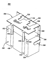
PIG. 7 is a ~.D~__L~ _ ~iew of filter 300 of EqG. 3 taken
together with shield 500 of P5Gs. 5 and 6. ESlter 300 and shield 500
0 together form the diele~ic filter assembly, referred to in the figure
by refer.,nce numeral 600, of the prefemd: ' ' ' of the present
...~. ' AB ' 1~ , because ofthe ' - of
first and second sheet portion~ 506 and 512 of shield 5ao, shield 500
may be l " - ' about iilter 300. AB " ' ' in the figure, first
sheet portion 506 seats ag~nst front side surfaoe 318 thidden from
Yiew in the ~ ' ' of ~IG. 7) to co~er the front side surface 318
thereby. Clip member~D 560 and 566 tODIY clip member 566 is shown in
~IG. 7) ~ erlgage with end side surfaces 330 and 336 of filt_r
300.
BecauDe ~econd llheet portion 5la of shield 500 e~tends at
an angle ~., ' ' to th~ plsnar direction deiined by first sheet
portion 506, second sheet portion 512 cvvers top surface 306 of filter
300. In contrast to the ' ' ', betwe~n iirst sheet portion 506
and front side surface 318 thi~den from view in P~G. 7) of filter 300
second sheet portion 512 is I ' ' at an ele~ation abo~e top
surface 306 by distance indicated by Une seg;nent 606.
n.; pror~ 542 and 548 which e~tend beyond an
edge side surface of second sheet porL~ion 512 seat against rear side
c_ 324 of filter 300. More ~ L.,..l~l.~ ,, prongs 542 and
548 ~ l~ engage with tches 426 and 432 formed to e~nd
along rear side surface 324. By proper selection of the depths of
notches 426 and 432 as well as the i' ' of prongs 542 and 548,
F~' - L - ~ e Of prongs 642 and 548 in such
with notches 426 and 432 permitD seating of the ~JL~ prong8
wo 94/02971 Pcr/US93/o--o
-16- 2118a93
witbin the notches 426 and 432 such that face surfsces of ~
prongs 642 and 548 are flush with, or are disposed beneath, the faoe
surfaoe of rear side surfaoe 324. Such p~ ~ pernuts surfaoe
l~lu~L..g of rear side surfaoe 324 upon a L ' ' ', such as a circuit
s board.
It is noted that, in the view of ~IG. 7, input and output
temlinals 612 and 618 disposed upon rear sides surfaoe 324 of filter
300, are also shown in the figure.
TuIDing ne~t to the side, ~~ view of ~IG. 8, the
0 dielectric filter assembly 600 of the preferred ~ ' ' of the
present ~.. i8 shown after seating of the assembly upon a
'1 here circuit board 640. Because ~ prongs 542 and
548 seat in r ' " _: ' with notches 426 and 43a of filter
300, rear side surfaoe 3a4 of filter 300 seats directly against circuit
board 640. Because filter assembly 600 may be l~urfaoe mounted upon
circoit board 640, the filter assembly may be coupled to an elect;ncal
circuit aisposed upon the circuit boara by a reflow so~der i
Clip member 560 (and al80 clip member 566, not ~own in the figure)
generates a cJipping force to clip the sbield ~00 in position about filter
300. A solder ~ may also be: rr ' ' ~ between filter 300
ana sbiela 500 to provide a po6itive electrical; i'
and also to assist in the ~ rr " of shield 500 to filter 300. Such
solder ~ is indicated in the figure by solder material 646.
~IG. 9 is a sectional view t~en 1 ~ through
filter assembly 600 and circuit board 640 of E IG. 8. The sectional ~iew
of ~IG. 9 again il' the ,~ ' ~' , between filter 300 and
sbield 500 of the filter assembly. The IG~ " ' ', between 1~
prong 648 of shield 500 ana notch 432 of filter 300 is also " ~ in
the figure. Because of such ~ ; _ _ t, rear side
surfaoe 324 of filter 300 is surface ''~ upon a circuit bo~ra 640.
Solder material 646 forming the solder - -- - - - ~ :- --- between first sheet
portion 506 of shield 500 and a side sur~aoe of filter 300 is ag~un
shown. b~ -'ly, solder material 652 used to form a solder
~, ,. . . ,p~ I r. between ~" .; g prong 548 and a surface of filter 300 i8
~ WO 94/02971 PCI'/US93/OS770 .
-17- 2118~9~
8180 shown. &ch solder /.--~..t~ . is for~ned for ressons similsr to
the ressons for r~ of the solder ~ I formed by solder
msterial ~i46.
Becsuse openings 530 snd 536 sre formed to estend
- s through second sheet por~ion 512, shield 500 msy be ~ 1 about
filter 300, snd sffised thereto, snd then ' " '~ tuned.
Openings 530 snd 536 peTmit access to the costing of c.,~l..~
msterisl formed upon a top ~l~rfsæ of the filter 300 thereby to permit
tuning of the filter. Onoe tuning o~ the filter hss been ~ ' d, the
0 same shield 500 msy be - ~ in the s~ised position sbout the
filter, snd the filter msy then be F: -' to be i to sn
electrical circuit.
Turning f~nally w to the block diagram of EIG. 10, a
radio . , referred to generally by reference numeral 700,
5 shown in block form. Radio . _. 700 i~ , for
essmple, of a radio ' ' ' - operative in a oellular,
l~yste~n. Radio i ._. 700 includes a filter assembly of the
preferred ' - ' of the present invention as a por~ion thereof.
A signal; ' to ~ . 750 is reoeived by
20 antenna 756, and a signal ~0,~ thereof is g ' on line
762 and applied to filter 768. F ilter 768 1. a f~ltered sign~ on
line 774 which iB applied to receiver c~rcuitry 778. Receiver circuitTy
778 performs functions such as ' ..~: .. and ~ ' '
of the reoeived sigl~al, as i8: . '- ' ~ ' ' circuitry 786
25 iB operative to modulate and .,~ in L ~, , a signal to be
- d by .. 750, and to generate a sigDal on line 730
which is applied to filter circuit 794. Filter circuit 794 is operative to
~enerate a filtered sigDal which is applied to antenna 756 by way of
line 762 to be i ' i'
SO A filter assembl~ of a preferred ' ~ ' of the
present invention may, for iDstsnoe, comprise f~lter 768 of ~_.
750 to be operative to filter a signal reoeived by the i . ~ .
While the prese~lt invention has been described in
r.~.. ~ I r with the prefeTred ~ ' shown in the various
WO 94/02971 PCI/US93/~0 ~
-18- 2118~3
figures, it is to be ~ d that other similar - ' " ' may be
u~ed and .- ..1; r.. .~ r .~ and addition~ may be made to the de~cnbed
for F- - f ~ e the same fimction of the pre~ent
invention wit hout denatu~ ~ r , the pre~ent
~.. ~hould not be limited to any ~ingle . ' " t, but rather
c~ L ~ in br~adth and ~cope in ~ ' with the re~itation of
the ,, ' ' ~laims.