Note: Descriptions are shown in the official language in which they were submitted.
~1186~9
INTERCONNECTION STRUCTURE OF ELECTRONIC PARTS
Background of the Invention
The present invention relates to an interconnection
structure of electronic parts and, particularly, to
an interconnection structure of electronic parts using
solder bumps.
By using an interconnection technology using
solder bumps, a number of connection terminals can be
interconnected at once. Therefore, such technology is
suitable for interconnecting electronic parts each having
a number of connection terminals and has been used widely
in interconnecting LSI chips having, for example, several
hundreds of connecting terminals.
It has been known that, in a case where a bare-chip
is connected to a substrate by using solder bumps, fault
of connecting portions occurs frequently. Bare-chip is
an LSI chip not covered with insulating material. The
reason for such fault is a difference in thermal expansion
coefficient between the LSI chip and the substrate on
which the LSI chip is mounted. The LSI chip generates
heat during its operation with which the LSI chip and the
substrate mounting the chip are expanded. Since thermal
expansion coefficients of them are different, stress is
generated in the solder bumps interconnecting the LSI
chip and the substrate. This stress is generated during
2I18fi49
- 2 -
operation of the LSI chip and disappears when the chip
is inoperative. Therefore, generation of stress in the
solder bumps is repeated, with which fatigue of the solder
bumps occurs, leading to destruction thereof. As a result,
the connecting portion or portions between the LSI chip
and the substrate shall be broken.
An example of technique for preventing such fault of
the interconnection structure is disclosed in N. Matsui,
et al. "VLSI CHIP INTERCONNECTION TECHNOLOGY USING STACKED
SOLDER BUMPS", pp. 573 to 578, Proc. IEEE 37th Electronic
Components Conf. In the technique disclosed in this
article, stress in the solder bumps is reduced by stacking
a plurality of solder bumps.
In this technique, however, the structure of the solder
bumps is very complicated and difficult to manufacture.
Summary of the Invention
An object of the present invention is to provide an
interconnection structure of electronic parts which is
simple in structure and manufacture and in which stress
to be generated in solder bumps is minimized.
In order to achieve the above object, each of solder
bumps constituting the interconnection structure is
provided-therein with a core member of metal.
In an embodiment of the present invention, each solder
bump having the core member is hourglass-shaped.
2118649
- 3 -
In another embodiment of the present invention, the
core member has a configuration which is variable according to
specific application thereof.
According to one aspect of the invention, there is
provided an interconnection structure for electronic parts,
comprising: solder bumps for providing electrical paths
between a first electronic part to a second electronic part,
each said solder bump being hourglass-shaped; and core members
provided in said solder bumps, respectively, wherein each of
said core members provides a portion only of each of said
electrical paths between said first electronic part and said
second electronic part .
According to another aspect of the present
invention, an interconnection method for interconnecting
electronic parts is provided, which comprises the first step
of mounting a core member on each pad of a first electronic
part, the second step of painting each pad of a second
electronic part with a predetermined amount of solder paste,
the third step of burying the core member in the solder paste
and the fourth step of heating and melting the solder paste,
cooling and solidifying it. The amount of solder paste, in
this method, is determined such that, when melted in the
fourth step, the solder paste provides an hourglass-shape by
surface tension.
According to a further aspect of the present
invention, an interconnection method for interconnecting
electronic parts is provided, which comprises the first step
66446-577
f
l 21 ~8S~g
- 3a -
of mounting a core member on each pad of a first electronic
part, the second step of inserting an annular shaped solder
into the core member, the third step of positioning the first
electronic part on a second electronic part such that the core
members are aligned with the respective pads of the second
electronic part and the fourth step of heating and melting the
annular solders, cooling and solidifying them, An amount of
solder forming each annular solder,
66446-577
~~.18~~9
- 4 -
in this method, is determined such that, when melted in
the fourth step, the solder provides an hourglass-shape
by surface tension.
A semiconductor device to be interconnected by using
the interconnection structure according to the present
invention includes a LSI bare-chip and core members
mounted on pads of the LSI bare-chip. Each core member
is given an amount of solder material which is enough to
form a hourglass-shaped solder bump is formed when reflown.
Brief Description of the Drawings
Other objects, features and advantages of the present
invention will become more apparent when the following
description is read in conjunction with the accompanying
drawings, wherein:
Fig. 1 shows an interconnection structure for
electronic parts, according to a first embodiment of
the present invention;
Fig. 2 shows a structure of a core member 4 in more
detail;
Figs. 3 and 4 show a method of manufacturing the
interconnection structure of electronic parts according
to the first embodiment of the present invention;
Figs: 5(a) and 5(b) show a simulation setting
condition for evaluating effectiveness of the inter-
connection structure according to the first embodiment
of the present invention;
211869
- 5 -
Fig. 5(c) shows a result of simulation for evaluating
effectiveness of the interconnection structure according
to the first embodiment of the present invention;
Fig. 6 shows a structure of a core member 4 according
to a second embodiment of the present invention;
Fig. 7 shows a method of manufacturing the inter-
connection structure for electronic parts, according to
a third embodiment of the present invention;
Fig. 8 shows a portion of an interconnection structure
for electronic parts, according to a fourth embodiment of
the present invention; and
Fig. 9 shows the interconnection structure for
electronic parts, accordin g to the fourth embodiment of
the present invention.
In these figures, same reference numerals depict
same constructive components, respectively.
Embodiment
(First Embodiment
A first embodiment of the present invention will be
described with reference to Fig. 1.
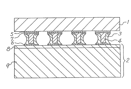
Referring to Fig. 1, in an interconnection structure
for electronic parts according to this embodiment, a
semiconductor chip 1 and a substrate 2 are interconnected
by solder bumps 3.
The semiconductor chip 1 is an LSI bare-chip. On one
2118fi49
- 6 -
surface of the semiconductor chip 1, a plurality of pads 5
are provided. These pads 5 are arranged in matrix. Each
pad 5 is constituted with laminated circular metal layers
each having diameter of 0.1 mm.
The substrate 2 includes a ceramic substrate 9 of
mainly almina and an organic insulating layer 8 provided
on the ceramic substrate 9. The organic insulating
layer 8 is provided on a surface of the ceramic substrate 9
which faces to the semiconductor chip 1. On the organic
insulating layer 8, a plurality of pads 6 are arranged
in matrix. The pads 6 on the organic insulating layer 8
correspond, in position; to the pads 5 on the semiconductor
chip 1, respectively. Each pad 6 is constituted with
laminated circular metal layers each having diameter of
0.1 mm.
The solder bumps 3 interconnect the pads 5 of the
semiconductor chip 1 and the pads 6 of the substrate 2
electrically and mechanically, respectively. Each solder
bump 3 in hourglass-shaped.
A core member 4 is provided in each solder bump 3.
The core member 4 is mounted on each pad 5 of the
semiconductor chip 1 by a solder 7. The solder 7
interconnects the pad 5 of the semiconductor chip 1
and the core member 4 electrically and mechanically.
Melting point of the solder 7 is higher than that of
a solder 10 forming the solder bump 3.
21 I 8;64 g
_7_
Configurations of the solder bump 3 and the core
member 4 will be described in detail referring to
Fig. 2 (a) ~ (c). Fig. 2 (a) ~ (c) shows the approximate
configuration of the core member 4. Exact size of each
portion of core member 4 is indicated by figures therein.
Referring to Fig. 2(a), the core member 4 is
constituted with a circular bottom portion 41 and a
circular pin portion 42. The bottom portion 41 and the
pin portion 42 are formed integrally. A diameter L1 of
the bottom portion 41 is 0.1 mm and a thickness L2 thereof
is 0.015 mm. Height L3 of the pin portion 42 is 0.0875 mm
and diameter L4 thereof is 0.047 mm. A vertical cross
section of a portion connecting the bottom portion 41 and
the pin portion 42 is rounded with radius R = 0.01 mm.
Referring to Fig. 2(b), diameter L8 of an upper and
lower ends of the solder bump 3 is 0.1 mm and diameter L5
of an intermediate portion of the solder bump 3 is 0.074 mm.
Height L6 of the solder bump 3 is 0.1 mm.
Referring to Fig. 2(c), distance L7 between a lower
end of the pin portion 42 and an upper surface of the pad 6
is 0.0125 mm.
Dimensions of the respective portions of the core
member 4 mentioned above may be changed within suitable
ranges, respectively. Height L3 of the pin portion 42
can be changed within a range from 0.05 mm to 0.1 mm,
diameter L4 of the pin portion 42 can be changed within
w..
~~~8~49
_8_
a range from 0.02 mm to 0.08 mm. Distance L7 between the
lower end of the pin portion 42 and the upper surface of
the pad 6 can be changed in a range from 0.01 mm to 0.02 mm.
Dimensions of the respective portions of the core member 4
should be set to values suitable for forming the solder
bump 3. Describing this in detail, the dimensions of the
respective portions of the core member 4 must be determined
such that the solder bump 3, when melted, becomes hourglass-
shape naturally by surface tension thereof. Therefore, the
dimensions of the respective portions of the core member 4
depend upon properties of the solder 10 forming the solder
bump 3.
Materials of the respective portions shown in Fig. 1
will be described.
The pads 5 and 6 are of gold or copper.
An example of material of the solder 7 is gold-tin
solder, whose melting point is higher than that of the
solder 10 forming the solder bump 3.
The core member 4 preferably satisfies the following
two conditions. The first condition is that the thermal
expansion coefficient of the material is smaller than that
of the solder 10 forming the solder bump 3. It has been
found by simulation that stress exerted on the connecting
portion is reduced when the material of the core member 4
satisfies this condition. Materials satisfying this
condition includes gold, silver, copper alloys, KUVAR,
etc.
2I~8~49
- 9 -
The second condition is that the Young's modulus
of the material is as great as possible. The first
condition has priority over the second one. In other
words, manufacturers applying this embodiment should
adopt the material that has biggest Young's modulusamong
the materials satisfying the first condition.
An example of the material of the solder 10 forming
the solder bump 3 is eutectic solder material of tin and
lead. The solder 10 must have melting point lower than
that of the solder 7.
Suitable combinations of materials of various
components mentioned above will be described.
When the material of the pad 5 is gold, the solder 7
is preferably a gold-tin solder. With this combination
of materials, wettability of the solder 7 is improved.
When the core member 4 is of gold or silver, the
solder 10 forming the solder bump 3 is preferably a tin-
lead eutectic solder. This is because thermal expansion
coefficient of the core member 4 becomes smaller than
that of the solder bump 3.
When the core member 4 is of gold or silver and the
solder 10 is of a tin-lead eutectic solder, the core
member 4 is preferably plated with copper in order to
prevent gold or silver from diffusing into the solder 10.
A method of forming the interconnection structure
shown in Fig. 1 will be described with reference to Figs.
3 and 4.
~. 2118fi4~
- 10 -
In the first step shown in Fig. 3, the core members 4
are mounted on the pads 5 of the semiconductor chip 1 by
reflowing the solder 7 painted on the pads 5. If necessary,
the core members 4 are preliminarily plated with suitable
material. This reflow-soldering is preferably performed
without using flux so that fault of the semiconductor chip 1
to be caused by flux is prevented. The reflow-soldering
without flux can be done in an atmospheric,gas such as
nitrogen, and argon.
In the second step shown in Fig. 4(a), the pads 6 on
the substrate 2 are painted with the solder 10 by using
screen printing. An amount of. the solder 10 for each
pad 6 is regulated such that the resultant solder bump 3,
when melted, becomes a hourglass-shape.
An optimum amount of the solder 10 for each pad 6
depends upon the material of the solder l0 and dimensions
of the respective portions of the core member 4.
Particularly, surface tension of the solder 10 when
melted is a basic factor to be used in determining the
optimum amount of the solder 10. The optimum amount of
the solder 10 is difficult to determine theoretically and
is determined according to experiments. If the amount of
the solder 10 is excessive, a resultant solder bump 3
becomes barrel-shape and, if it is short, the upper portion
of a resultant solder bump 3 becomes small relatively. It
can be said qualitatively that the larger the diameter L4
21I8fi49
- 11 -
of the pin portion 42 of the core member 4 requires the
larger amount of solder 10.
In the third step shown in Fig. 4(b), the core
members 4 are inserted into the respective solders 10
while regulating the position of the semiconductor chip 1
with respect to the substrate 2 such that there is provided
a predetermined distance between the lower ends of the pin
portions of the core members 4 and the upper surfaces of
the pads 6.
In the fourth step shown in Fig. 4(c), the solders 10
are reflown. First, the solders 10 are heated while
maintaining the semiconductor chip 1 and the substrate 2
horizontally, to melt the solders. Each solder 10 in
molten state is pulled up by the effect of surface tension
and is shaped to an hourglass configuration. Thereafter,
the solders 10 are cooled and solidified. The solidified
solders 10 have hourglass configurations.
Now, a result of simulation performed to evaluate the
effectiveness of this embodiment will be described with
reference to Fig. 5.
In this simulation, stress characteristics of a
single solder bump 3 was simulated, as shown in Fig. 5(a).
A position of the single solder bump 3 was set in around
the outermost periphery of the substrate 2. Values of
the respective members were set as shown in Fig. 5(b).
Stress in the solder bump 3 was regarded as 0 at a
2118649
- 12 -
temperature of 23°C and stress in the solder bump 3
maintained at 125°C was simulated according to the
finite-element method under these condition. For a
comparison purpose of the characteristics, stress
characteristics of the interconnection structures using
solder bumps having different configuration from that
of the solder bump 3 were also simulated. In more detail,
(i) a barrel-shaped solder bump, (ii) an hourglass-shaped
solder bump having no core member 4, (iii) only the core
member 4 and (iv) the solder bump 3 of this embodiment
were simulated, respectively. Fig. 5(c) shows a result
of the simulation.
In Fig. 5(c), a portions of each solder bump in which
maximum principal stress becomes maximum is indicated by
max. This stress is referred to as maximum stress, hereinafter.
Stress ratio which is a ratio of maximum stress between the
respective solder bump structures is set to 1 for the solder bump
structure (i). As a result, stress ratio of the solder
bump structure (ii) is 0.62 and that of the solder bump
structure (iii) is 0.63. Stress ratio of the solder bump 3
of the present invention is 0.51. That is, it was proved
that stress acting on the solder bump 3 of this embodiment
during a time period in which temperature rises is smaller
compared with other solder bump structures.
In this embodiment, the core member 4 is provided
in the solder bump 3 as mentioned. With such structure,
~1~8~49
- 13 -
it is possible to reduce stress generated in the solder
bump during a time period in which temperature rises.
Further, the interconnecting structure of this embodiment
is simple in construction and can be easily manufactured.
Second Embodiment
A second embodiment of the present invention will be
described with reference to Fig. 6. A feature of this
embodiment resides in the structure of the core member 4.
Figs. 6(a) to 6(f) show six different structures of
the core member 4.
The structure shown in Fig. 6(a) is the structure of
the core member 4 used in the first embodiment.
The structure shown in Fig. 6(b) has a pointed pin
portion 42.
In the structure shown in Fig. 6(c), the pin portion 42
has a elliptic horizontal cross section. This structure is
effective when applied to a case where an interval between
adjacent pads 5 and hence adjacent pads 6 is small.
In the structure shown in Fig. 6(d), the pin portion 42
has a hole 425. In this structure, it is possible to
provide a stronger connection than the structure shown in
Fig. 6(a) since the solder 10 in molten state invades to
the hole 425.
In the structure shown in Fig. 6(e), the pin portion 42
is constituted with a pin portion 421 and a pin portion 422
with a gap provided therebetween. In this structure, it is
....
~1~8699
- 14 -
possible to provide a stronger connection than the structure
shown in Fig. 6(a) since the solder 10 in molten state
fills the gap.
In the structure shown in Fig. 6(f), the pin portion 42
is constituted with four pin portions 421, 422, 423 and 424
with a gap being provided adjacent ones of these pin
portions. In this structure, it is possible to provide a
stronger connection than the structure shown in Fig. 6(a)
since the solder 10 in molten state dills these gaps.
In this embodiment, the core members 4 having various
configurations are used. Selection of any one of these
structures should be made according to situation to which
it is applied. It is possible to use any combination of
these pin portion structures. For example, by combining
the structures shown in Fig. 6(b) and Fig. 6(e), the pin
portions 421 and 422 of the structure in Fig. 6(e) shall
be pin-pointed, respectively.
Third Embodiment
A third embodiment of the present invention will be
described with reference to Fig. 7. A feature of this
embodiment resides in method of forming the solder bump
which is used in the first embodiment.
The first step of this embodiment is the same as the
first step in the first embodiment.
In the second step shown in Fig. 7(a), solder rings 11
are fitted on the pin portions 42 of the respective core
2~~ss4~
- 15 -
members 4 by inserting the pin portions into center
holes 111 of the solder rings 11. An amount of the
solder ring 11 is determined such that the solder ring 11,
when melted, becomes an hourglass-shaped solder bump 3.
In the third step shown in Fig. 7(b), the semiconductor
chip 1 is positioned on the substrate 2 and is aligned
therewith with a predetermined gap between the top ends
of the pin portions 42 and the upper surfaces of the pads 6.
In the fourth step shown in Fig. 7(c), the solder
rings 11 are reflown. This step is the same as the fourth
step in the first embodiment. The solder bumps 3 having
hourglass-shaped configurations are obtained after the
fourth step.
In this embodiment, since the solder rings 11 each
of an optimum amount of solder are fitted on the pin
portions 42, respectively, there is no need of regulating
the amount of solder to paint the pads 6. Further, the
solder ring itself can be a commercial product. A purchaser
is not required to regulate the amount of solder.
(Fourth Embodiment
A fourth embodiment of the present invention will be
described with reference to Figs. 8 and 9. A feature of
this embodiment resides in the structure of the substrate 2.
In this embodiment, the core members 4 are provided on the
pads 6 on the substrate 2.
Referring to Fig. 8, the substrate 2 of this embodiment
~1~8649
- 16 -
is constituted with only the ceramic substrate 9. On the
upper surface of the ceramic substrate 9, the pads 6 are
arranged and the core members 4 are mounted on the pads 6,
respectively. The core member 4 is soldered to the pad 6
by the solder 7: Structures and materials of the pad 6,
the solder 7 and the core member 4 are the same as those
in the first embodiment, respectively.
In a state where the semiconductor chip 1 and the
substrate 2 are connected as shown in Fig. 9, the pads 5
and the pads 6 are connected by the solder bumps 3 each
having an hourglass-shaped configuration.
In this embodiment, the core members 4 are provided
on the substrate 2. The effects to be achieved by the
fourth embodiment are the same as those achieved by the
first embodiment.
Other Embodiment s
A first feature of the present invention resides in
that the core members 4 are provided in the solder bumps 3,
respectively. A second feature of the present invention
resides in that the core members 4 are provided in the
hourglass-shaped solder bumps 3, respectively. A third
feature of the present invention resides in that the
solder bumps 3 are made hourglass-shaped by utilizing
surface tension. Further, a fourth feature of the present
invention resides in that the configuration of the core
member 4 is changed according to its use. A fifth feature
~~~8i~4~
- 17 -
of the present invention resides in that the solder ring 11
is fitted on the pin portion 42 of the core member 4.
A sixth feature of the present invention resides in that
the core members 4 are provided on the substrate 2.
The present invention is featured by these features
and can be embodied in various other manners than described.
For example, it is possible to combine the features of the
first to sixth embodiments. Further, the interconnection
structure of the present invention can be used other
applications than the connection of the LSI bare-chip.
In the present invention, the amount of solder forming
a solder bump and the configuration of core member should
be changed suitably according to a situation to which the
present invention is applied. Further, the solder ring
itself can be a commercial product. A purchaser is not
required to regulate the amount of solder.
The scope of the present invention is indicated by
the appended claims, but not restricted in any way by the
text of the specification. Furthermore, all modifications
and changes which come within the range of equivalency in
the claims are intended to be embraced therein.