Note: Descriptions are shown in the official language in which they were submitted.
~qo~(~A~l)
2119073
TITLE OF THE INVENTION
DATA TRANSMISSION SYSTEM
FOR AUTOMOTIVE VEHICLES
BACKGROUND OF THE INVENTION
Field of the Invention
This invention relates to a data transmission
system for an automotive vehicle, which comprises a
plurality of electronic control units installed on the
vehicle and a common communication line connecting the
electronic control units with each other.
Prior Art
Recently, automotive vehicles are electronically
controlled in respect of most part of the engine
control, the suspension control, and so on.
Accordingly, they are each equipped with a data
transmission system for connecting a plurality of
electronic control units (hereinafter referred to as
~the ECU's~) for the respective types of control by a
common communication line (hereinafter referred to as
~the network bus") to transmit data necessary for the
above types of control to each other by the use of
asynchronous serial data signals.
High reliability is demanded of this type of
data transmission system for automotive vehicles, and
therefore, the system employs a twisted-pair
transmission method in which the network bus is
implemented by a composite signal line formed by a
twisted-pair transmission line having a pair of signal
lines to which a sending end (ECU) delivers digital
data signals having opposite polarities (i.e. being
opposite in phase), respectively, so that a receiving
2119073
end (ECU) can receive a message from the sending end
based on changes in the polarities of the signals
indicative of the logical states of the signals. The
twister-pair transmission method makes it possible to
transmit data even if one of the pair of signal lines
is disconnected, thereby enhancing reliability of the
system.
However, the twisted-pair transmission method is
capable of transmitting data even if one of the twisted
pair is disconnected, for example, as described above.
Therefore, it is neither possible to recognize
occurrence of the fault nor to determine which of them
is faulty due to disconnection, ground fault, or the
like, which prevents the system from recovering from
the fault. Therefore, when the other of the twisted-
pair, which has been safe, becomes faulty, it is
entirely impossible for the system to perform data
transmission.
Further, within such a conventional data
transmission system, a receiving end (ECU) is required
to perform synchronization of bit times by making the
phase of a bit time of a serial data signal received
from the network bus and the phase of a bit time within
the receiving end synchronous with each other, as well
as to perform resynchronization by temporarily lengthen
or shorten the bit time within the receiving end to
correct a difference in phase of the bit time within
the receiving end from the bit time of the received
serial data signal with which the bit time within the
receiving end was already made synchronous, so as to
always ensure correct demodulation of the serial data
signal.
Conventionally, as shown in Fig. 8a and Fig. 8b,
the resynchronization is permitted only when the
logical state of the serial data signal has changed
21~9073
within each synchronizing time period (see Fig. 8b at a
time point tl), to prevent the system from being
susceptible to noises.
However, there is usually a slight difference
between the reference clock frequency of a sending end
(ECU) and that of a receiving end (ECU), so that when
the serial data signal continues to be in the same
logical state, the difference can be accumulated to
such an extent as will cause a point of change in the
logical state of the serial data signal to fall outside
a corresponding resynchronizing time period (see Eig.
8b at a time point t3), causing the bit time of the
receiving end to be out of phase.
If each synchronizing time period is set to a
longer duration for prevention of such a problem, there
now arises an inconvenience of a higher possibility of
erroneous resynchronization caused by noises or the
like.
SUMMARY OF THE INVENTION
It is a first object of the invention to provide
a data transmission system for an automatic vehicle for
transmitting data between a plurality of electronic
control units via a transmission line formed by a pair
of signal lines, by a sending end delivering digital
data signals having opposite polarities to the
respective signal lines, which is capable of detecting
a fault occurring to one of the pair of signal lines
and determining which of them is faulty.
It is a second object of the invention to
provide a data transmission system which is capable of
performing accurate resynchronization of the bit times
even when the serial data signal continues to be in the
same logical state.
21 1 9073
In accordance with the present lnvention, there is
provided in a data transmission system for an automotive
vehicle, lncluding a plurality of control units installed on
said vehicle, and a transmission line connecting said
plurality of control units with each other, said transmission
line comprlsing a pair of signal llnes to whlch dlgltal data
slgnals havlng opposlte polarltles are dellvered for
transmission of data,
the improvement wherein each of sald plurallty of control
unlts comprlses
flrst recelvlng means for recelvlng both of sald dlgltal
data slgnals havlng opposite polaritles, and for outputtlng a
first difference signal indicative of a difference between
sald dlgltal data slgnals;
second receiving means for recelving one of said digital
data slgnals, and for outputting a second dlfference slgnal
lndlcative of a dlfference between sald one of sald digital
data signals and a predetermlned reference level set thereto;
thlrd recelvlng means for recelvlng the other of sald
dlgltal data slgnals, and for outputtlng a thlrd dlfference
slgnal lndicatlve of a difference between the other of said
digltal data slgnals and a predetermlned reference level set
thereto; and
fault-detectlng means for detectlng whlch of sald palr of
slgnal llnes is faulty, based on said first dlfference slgnal
output from sald flrst recelvlng means, sald second dlfference
signal output from said second receiving means, and said third
difference slgnal output from sald thlrd receivlng means.
B 70668-39
- . ,
21 1 9073
4a
Preferably, the fault-detectlng means comprlses a
flrst excluslve OR clrcult for outputtlng a flrst detection
slgnal lndicatlve of an excluslve OR of the flrst dlfference
signal output from the flrst recelvlng
70668-3g
B
2119073
means and the second difference signal output from the
second receiving means, and a second exclusive OR
circuit for outputting a second detection signal
indicative of an exclusive OR of the first difference
signal output from the first receiving means and the
third difference signal output from the third receiving
means, and wherein the fault-detecting means detects
which of the pair of signal lines is faulty, based on
the first detection signal output from the first
exclusive OR circuit and the second detection signal
output from the second exclusive OR circuit.
More preferably, the fault-detecting means
detects which of the pair of signal lines is faulty, at
or in the vicinity of a center of each bit time of the
digital data signals.
Further preferably, the fault-detecting means
includes a timing clock pulse generator for generating
predetermined timing clock pulses at or in the vicinity
of the center of each bit time of the digital data
signals, a first sampling circuit for being supplied
with the first detection signal from the first
exclusive OR circuit and the predetermined timing clock
pulses from the timing clock pulse generator, for
sampling of the first detection signal in response to
the predetermined timing clock pulses, and a second
sampling circuit for being supplied with the second
detection signal from the second exclusive OR circuit
and the predetermined timing clock pulses from the
timing clock pulse generator, for sampling of the
second detection signal in response to the
predetermined timing clock pulses.
The above and other objects, features, and
advantages of the invention will become more apparent
from the following detailed description taken in
conjunction with the accompanying drawings.
2119073
BRIEF DESCRIPTION OF THE DRAWINGS
Fig. 1 is a block diagram showing the whole
arrangement of a data transmission system for an
automotive vehicle, according to an embodiment of the
invention;
Fig. 2 is a block diagram showing the
arrangement of one of electronic control units
appearing in Fig. l;
Fig. 3 is a circuit diagram showing details of a
bus interface and a network bus both appearing in Fig.
2;
Fig. 4a to Fig. 4i form a timing chart which is
useful in explaining the operation of the data
transmission system for detecting a fault of the
network bus, when the speeds of response of receivers
are identical to each other, in which:
Fig. 4a shows a signal applied to a sending
terminal T2 appearing in Fig. 3;
Fig. 4b shows a signal applied to a sending
terminal Tl appearing in Fig. 3;
Fig 4c shows a signal appearing on one signal
line A of a twisted-pair transmission line appearing in
Fig. 3;
Fig. 4d shows a signal appearing on the other
signal line B of the twisted-pair transmission line
appearing in Fig. 3;
Fig. 4e shows an output signal RX-D from a
differential receiver 111 appearing in Fig. 3;
Fig. 4f shows an output signal RX-l from an A
receiver 121 appearing in Fig. 3;
Fig. 4g shows an output signal RX-2 from a B
receiver 126 appearing in Fig. 3;
Fig. 4h shows an input signal to an A fault-
21i9073
detecting terminal T4 appearing in Fig. 3; and
Fig. 4i shows an input signal to a s fault-
detecting terminal T5 appearing in Fig. 3;
Fig. 5a to Fig. 5i form a timing chart which is
useful in explaining the operation of the data
transmission system for detecting a fault of the
network bus, when the speeds of response of the
receivers are different from each other, in which:
Fig. 5a shows the signal applied to the sending
terminal T2;
Fig. 5b shows the output signal RX-D from the
differential receiver 111;
Fig. 5c shows the output signal RX-l from the A
receiver 121;
Fig. 5d shows the output signal RX-2 from the B
receiver 12 6;
Fig. 5e shows an output from an A exclusive "OR"
circuit 131 appearing in Fig. 3; and
Fig. 5f shows an output from a B exclusive "OR"
circuit 133 appearing in Fig. 3;
Fig. 5g shows the timing of sampling clock
pulses;
Fig. 5h shows the input signal to the A fault-
detecting terminal T4; and
Fig. 5i shows the input signal to the B fault-
detecting terminal T5;
Fig. 6a to Fig. 6c form a timing chart which is
useful in explaining the construction of one bit time,
in which:
Fig. 6a shows timing clock pulses;
Fig. 6b shows an asynchronous serial signal; and
Fig. 6c shows bit segments of bits in a
receiving end;
Fig. 7 is a flowchart showing a procedure of
synchronizing/resynchronizing processing according to
2119073
the embodimenti
Fig. 8a to Fig. 8c form a timing chart which is
useful in explaining a manner of setting a
resynchronizing time period, in which:
Fig. 8a shows the asynchronous serial signal;
Fig. 8b shows bit segments of bits in the
receiving end according to the prior art; and
Fig. 8c shows bit segments of bits in a
receiving end according to the embodiment of the
invention.
DETAILED DESCRIPTION
The invention will be described in detail with
reference to drawings showing an embodiment of the
lnventlon .
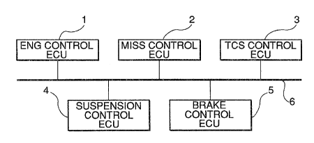
Fig. l schematically shows the arrangement of a
data transmission system for an automotive vehicle
according to the embodiment. The data transmission
system comprises electronic control units (hereinafter
referred to as "the ECU's") l to 5 connected with each
other via a network bus 6. An ENG control ECU l
controls operation of an engine in response to
operation of an accelerator pedal operated by a driver
of the vehicle, etc. An MISS control ECU 2 controls an
automatic transmission of the vehicle depending on the
operating conditions of the engine. A TCS control ECU
3 detects a slip of driving wheels and controls an
output torque of the engine. A suspension control ECU
4 controls a suspension (active suspension) system of
the vehicle depending on the operating conditions of
the engine. A brake control ECU 5 detects a slip of
wheels and controls braking operation. These ECU's l
to 5 are required to be permitted to mutually monitor
control parameters determined by the ECU's and
2119073
operating parameters detected by sensors, some of the
sensors being collectively shown in Eig. 2, and hence
are connected to each other by the network bus 6 for
transmission of data necessitated by each other.
Fig. 2 shows the arrangement of the ENG control
ECU 1 which comprises a central processing unit
(hereinafter referred to as "the CPU") 101, an
input/output interface 104 by way of which a plurality
of sensors 11, and a plurality of actuators, such as
fuel injection valves, are connected to the CPU 101.
The CPU 101 is connected via a bus line 107 to a RAM
(Random Access Memory) 102, a ROM (Read Only Memory)
103, and a communication control IC (Integrated
Circuit) 105. The communication control IC 105 is
connected via a bus interface 106 to the network bus 6.
The CPU 101 determines control parameters based
on output signals from the sensors 11 according to
programs stored in the ROM 103 to drive the actuators
12. The RAM 102 temporarily stores data of results of
computation therein. The communication control IC 105
controls transmission of a message to the network bus
and reception of a message from the network bus.
Fig. 3 shows details of the network bus 6 and
the bus interface 106 connected to the communication
control IC 105. The network bus 6 is formed by a
twisted-pair transmission line comprised of a signal
line A being connected to a power supply line VSUP to
have its potential pulled up and having terminating
resistances 6a, and a signal line B having its
potential not pulled up, and having terminating
resistances 6b.
The communication control IC 105 has a first
sending terminal T1 connected to a base of a transistor
119 via a resistance 115. The transistor 119 has an
emitter thereof connected to the power supply line
2119073
VSUP, and a collector thereof connected to a non-
inverting input terminal of a first comparator
(hereinafter referred to as "the differential
receiver~) 111 via a capacitor 141 for extracting an
amount of change in amplitude of the signal on the
signal line B, a non-inverting input terminal of a
second comparator (hereinafter referred to as "the B
receiver~) 126, and the signal line B of the twisted-
pair transmission line, by way of a resistance 116.
The communication control IC 105 has a second
sending terminal T2 connected to a base of a transistor
120 via a resistance 117. The transistor 120 has an
emitter thereof grounded, and a collector thereof
connected to an inverting input terminal of the
differential receiver 111 via a capacitor 142 for
extracting an amount of change in amplitude of the
signal on the signal line A, an inverting input
terminal of a third comparator (hereinafter referred to
as "the A receiver') 121, and the signal line A of the
twisted-pair transmission line, by way of a resistance
118.
The inverting input terminal of the differential
receiver 111 is connected via a resistance 112 to the
power supply line VSUP, and also via a resistance 113
to the non-inverting input terminal of the differential
receiver 111. The differential receiver 111 has its
non-inverting input terminal grounded via a resistance
114, and delivers an output signal RX-D therefrom to a
differential receiving terminal 13 of the communication
control IC 105.
The inverting input terminal and the non-
inverting input terminal of the A receiver 121 are
connected to a voltage divider formed by resistances
122 and 123 for dividing voltage of the power supply
line VSUP, and a voltage divider formed by resistances
2119073
124 and 125 for dividing same, respectively. The A
receiver 121 compares voltage (corresponding to the
logical state) of a signal on the signal line A of the
twisted-pair transmission line applied to the inverting
input terminal thereof with a reference voltage
determined by the resistances 124 and 125 of the
voltage divider and applied to the non-inverting input
terminal thereof, and delivers a difference signal RX-1
indicative of a difference (i.e. results of the
comparison) therebetween to one input terminal of a
first exclusive ~OR~ gate (hereinafter referred to ~the
A exclusive ~OR~ circuit) 131.
The A exclusive ~OR~ circuit 131 has the other
input terminal thereof supplied with the output signal -
RX-D from the differential receiver 111, and delivers
an output signal (detection signal) to a first sampling
circuit 132 which samples the output signal from the A
exclusive ~OR~ circuit 131, bit by bit, based on
predetermined sampling clock pulses CLK supplied from a
sampling clock pulse generator, not shown. The first
sampling circuit 132 delivers its output signal to an A
fault-detecting terminal T4 of the communication
control IC 105.
The non-inverting input terminal and the
inverting input terminal of the B receiver 126 are
connected to a voltage divider formed by resistances
127 and 128 for dividing voltage of the power supply
line VSUP, and a voltage divider formed by resistances
129 and 130 for dividing same, respectively. The B
receiver 126 compares voltage (corresponding to the
logical state) of a signal on the signal line B of the
twisted-pair transmission line applied to the non-
inverting input terminal thereof with a reference
voltage determined by the resistances 129 and 130 and
applied to the inverting input terminal thereof, and
211!~073
delivers a difference signal RX-2 indicative of a
difference (i.e. results of the comparison)
therebetween to one input terminal of a second
exclusive "OR" gate (hereinafter referred to ~the B
exclusive "OR" circuit) 133.
The B exclusive "OR" circuit 133 has the other
input terminal thereof supplied with the output signal
RX-D from the differential receiver 111, and delivers
an output signal (detection signal) to a second
sampling circuit 134 which samples the output signal
from the B exclusive ~OR~ circuit 133, bit by bit,
based on the predetermined sampling clock pulses CLK.
The second sampling clock 133 delivers its output
signal to a B fault-detecting terminal T5 of the
communication control IC 105.
The first and second sending terminals Tl, T2 of
the communication control IC 105 are supplied with
pulse signals opposite to each other in phase. When
the first sending terminal Tl is at a low level (the
logical state "0") and the second sending terminal T2
is at a high level (the logical state ~ ), both the
transistors 119 and 120 are turned on to set the
logical state of the signal on the signal line B of the
twisted-pair transmission line to ~ and the logical
state of the signal on the signal line A of the
twisted-pair transmission line to "0". When the first
sending terminal Tl is at a high level and the second
sending terminal T2 is at a low level, both the
transistors 119 and 120 are turned off to set the
logical state of the signal on the signal line B to "0"
and the logical state of the signal on the signal line
A to "1". Thus, a sending end (e.g. ENG ECU) sends out
signals opposite in phase to each other, to the signal
lines A and B of the twisted-pair transmission line
forming the network bus, respectively .
21~9073
As can be presumed from the above, the logical
state of the output signal RX-D from the differential
receiver 111 becomes equal to "0" or ~ , as the
logical state of the signal on the signal line A of the
twisted-pair transmission line becomes equal to "1" or
~0~ (i.e. as the logical state of the signal on the
signal line B becomes equal to ~0" or "1~), whereby a
message loaded on the network bus 6 is received.
The ECU's 2 to 5 are basically constructed in
the same manner. Therefore, even if one of the ECU's
sends out a signal which sets the logical state of the
signal on signal line s to ~0~ (i.e. sets the logical
state of the signal line A to "1~), when another ECU
sends out a signal which sets the logical state of the
signal line B to ~ , the logical state of the signal
on the signal line B is set to ~ . Therefore, in the
present embodiment, a state in which the signal on the
signal line B is at the high level (i.e. the logical
state thereof is equal to ~ ) and hence the signal on
the signal line A is at the low level (i.e. the logical
state thereof is equal to "0") is defined as a dominant
state, and an opposite state thereof as a recessive
state.
Next, the operation of the present system for
detecting a fault, such as a disconnection or a short-
circuit, of the network bus 6 will be described with
reference to a timing chart shown in Fig. 4a to Fig. 4i
and one shown in Fig. 5a to Fig. 5i. Fig. 4a to Fig.
4i correspond to an ideal case in which the speed of
response of the differential receiver 111 is equal to
that of the A receiver 121 and that of the B receiver
126, whereas Fig. 5a to Fig. 5i correspond to a case in
which the speed of response of the differential
receiver 111 is different from that of the A receiver
121 and that of the B receiver 126.
2119073
Referring to the timing chart of Fig. 4a to Fig.
4i, when the sending terminals Tl and T2 are supplied
with transmitter signals having polarities opposite to
each other, as shown in Fig. 4b and Fig. 4a,
respectively, signals having polarities opposite to
those of the sending terminals Tl and T2, respectively,
as shown in Fig. 4d and Fig. 4c, appear on the signal
lines B and A of the twisted-pair transmission line
through operations of the transistors ll9 and 120,
provided that the network bus 6 is not faulty.
However, if the pulled-up signal line A of the
twisted-pair transmission line suffers from a
disconnection or a ground fault at a point indicated by
a circle of the broken line in Fig. 3, for example, the
signal on the signal line A of the twisted-pair
transmission line is held at the logical state "l" or
"0" irrespective of the logical states of the
transmitter signals (see Fig. 4c), and the signal on
the signal line B of the twisted-pair transmission
signal is opposite in polarity to the transmitter
signal applied to the sending terminal Tl (see Fig.
4d).
In contrast, if the non-pulled-up signal line B
of the twisted-pair transmission line suffers from a
disconnection or a ground fault at a point indicated by
a circle of the broken line in Fig. 3, for example, the
signal on the signal line B of the twisted-pair
transmission line is held at the logical state "0"
irrespective of the logical states of the transmitter
signals (see Fig. 4d), and the signal on the signal
line A of the twisted-pair transmission line is
opposite in polarity to the transmitter signal on the
sending terminal T2 (see Fig. 4c).
On the other hand, the output signal RX-D from
the differential receiver lll always has the same
2119073
polarity as the transmitter signal applied to the
sending terminal T2, as shown in Fig. 4e, irrespective
of whether the signal line A or B of the twisted-pair
transmission line suffers from a disconnection or a
ground fault. That is, even if one of the signal line
A or B of the twisted-pair transmission line suffers
from a disconnection or a ground fault, it is possible
for other ECU's to normally receive the message sent
out from the present ECU.
If the signal line A suffers from a
disconnection or a ground fault at the point indicated
by the circle of the broken line as shown in Fig. 3,
for example, the signal on the signal line A connected
to the inverting input terminal of the A receiver 121
is held high or low (i.e. the logical state thereof is
equal to "1" or ~'0"), and the output signal RX-l from
the A receiver 121 iS held low or high (i.e. the
logical state thereof is equal to "0" or "1") (see Fig.
4f), accordingly.
Further, if the signal line B suffers from the
disconnection or ground fault at the point indicated by
the circle of the broken line as shown in Fig. 3, for
example, the signal on the signal line B applied to the
B receiver 12 6 is held low (i.e. the logical state
thereof is equal to "0"), so that the output signal RX-
2 from the B receiver 126 is held low (i.e. it is in
the logical state ~0") (see Fig. 4g).
The A exclusive "OR" circuit 131 delivers a
signal indicative of the exclusive " OR " of the output
signal RX-l from the A receiver 121 and the output
signal RX-D from the differential receiver 111, which
goes high (i.e. enters the logical state "1") only when
the signal line A suffers from a disconnection or a
ground fault, as shown in Fig. 4h, via the first
sampling circuit 132 to the A fault-detecting terminal
2119~73
16
T4. Therefore, the communication control IC 105 can
recognize that the signal line A of the twisted pair
transmission line is faulty, when the signal applied to
the A fault-detecting terminal T4 goes high (i.e.
enters the logical state ~
On the other hand, the B exclusive " OR " circuit
133 delivers a signal indicative of the exclusive "OR"
of the output signal RX-2 from the B receiver 126 and
the output signal RX-D from the differential receiver
111, which goes high (i.e. enters the logical state
~1") only when the signal line B suffers from a
disconnection or a ground fault, as shown in Fig. 4i,
via the second sampling circuit 134 to the B fault-
detecting terminal T5. Therefore, the communication
control IC 105 can recognize that the signal line B of
the twisted pair transmission line is faulty, when the
signal applied to the B fault-detecting terminal T5
goes high (i.e. enters the logical state "1").
In this manner, the communication control IC 105
is capable of determining which of the signal lines A
and B of the twisted-pair transmission line is faulty.
However, if the speed of response of the
differential receiver 111 is different from the speed
of response of the A receiver 121 or that of the B
receiver 126, resulting in a difference in timing of
generation of the output signals RX-D, RX-l, and RX-2,
as shown in Fig. 5b, Fig. 5c, and Fig. 5d, the A
exclusive "OR" circuit 131 and the B exclusive "OR"
circuit 133 generates pulses at points of change in the
logic of the signal bits, as shown in Fig. 5e or Fig.
5f, which can cause the communication control IC 105 to
erroneously determine that the twisted-pair
transmission line is faulty.
Therefore, in the present embodiment, pulses of
the sampling clock CLK, which are generated at or in
2119073
the vicinity of the center of each bit time, are
supplied to the first and second sampling circuits 132
and 13 4, as shown in Fig. 5g, which sample the output
signals from the A exclusive ~OR~ circuit 131 and the B
exclusive ~OR" circuit 133, respectively, in response
to the predetermined timing clock pulses CLK to avoid
generating the erroneous pulses described above.
Thus, the first and second sampling circuits 132
and 134 perform sampling of only the output signals
from the A exclusive ~OR~ circuit 131 and the B
exclusive ~OR~ circuit 133, bit by bit, which correctly
indicate a fault of the twisted-pair transmission line,
if any, and deliver output signals to the A fault-
detecting terminal T4 and the B fault-detecting
terminal T5, as shown in Fig. 5h and Fig. 5i, thereby
preventing occurrences of the erroneous detection of a
fault in the twisted-pair transmission line. In this
connection, although Fig. 5 shows a case in which the
signal line A of the twisted-pair transmission line
suffers from a ground fault, it goes without saying
that erroneous detection of a disconnection of the
signal line A, or a disconnection or a ground fault of
the signal line B, can be prevented, in the same
manner.
Next, a method of data transmission between the
ECU~s will be described. In the present embodiment, a
token passing method is employed. This takes into
consideration the fact that compared with a CSMA/CD
(Carrier Sense Multiple Access with Collision
Detection) method which is capable of settling the
collision, the token passing method is advantageous in
respect of an electric delay on the network bus, and is
capable of easily determining the maximum message delay
time period, allowing the network system to be designed
easily.
211907~
The construction of each bit corresponding to
one bit time used in the present embodiment will be
described with reference to Fig. 6a to Fig. 6c.
Fig. 6a shows reference timing clock pulses, and
Fig. 6b shows an asynchronous serial signal received.
As shown in Fig. 6c, in the present embodiment, one bit
is divided into four segments SEGl to SEG4.
The segment SEGl corresponds to a section within
which an edge (a point of change in the logic) of the
serial signal should occur, the segment SEG2 to a first
section for synchronization or resynchronization, the
segment SEG3 to a section for sampling, and the segment
SEG4 to a second section for resynchronization. The
segment SEGl has a duration of one clock time (a
repetition period of the timing clock pulse), and the
segments SEG2 to SEG4 have respective durations longer
than one clock time. Therefore, the segments SEG4,
SEGl and SEG2 determine a time period for
resynchronization (resynchronizing time period).
Fig. 7 shows a program for performing the
synchronizing/resynchronizing processing executed
according to the present embodiment. This processing
is started upon starting reception of a message (more
specifically, when one dominant bit indicative of the
start of a message is detected).
First, at a step S1, a same logic bit sequence
counter, not shown, for counting the number of
sequential or successive bits having the same logic is
reset, and then the resynchronizing time period is set
to an initial value at a step S2, followed by resetting
a bit segment counter, not shown, for counting the
number of timing clock pulses corresponding to one bit
time at a step S3. Upon resetting of the bit segment
counter, the synchronization is effected (see Fig. 8a
and Fig. 8c). At the following step S4, it is
21~9073
19
determined whether or not an edge of the serial signal
has been input or detected.
When the step S4 is first carried out, the edge
cannot be input, and hence the program proceeds to a
step S6, where it is determined whether or not the
count value of the bit segment counter is equal to a
final value. In this connection, the final value of
the bit segment counter means a count value
corresponding to the lapse of one bit time. When this
step is first carried out, the answer to this question
is negative (NO), and the bit segment counter is
increased by an incremental value at a step S7,
followed by the program returning to the step S4. If
an edge of the serial signal is input or detected (see
Fig. 8c at a time point tl designated by Fig. 8a),
during execution of cycles of the steps S4, S6, and S7,
the program proceeds from the step S4 to a step S5,
where it is determined whether or not the count value
of the bit segment counter is within a corresponding
resynchronizing time period (corresponding to a total
duration of the segment 4, the segment l, and the
segment 2). If the answer to this question is
affirmative (YES), the program returns via the steps Sl
and S2 to the step S3, where the bit segment counter is
reset to perform resynchronization. If the answer is
negative (NO), the program returns to the step S6.
If the answer to the question of the step S6
becomes affirmative (YES), during execution of cycles
of the steps S4, S6, and S7, i.e. if the count value of
the bit segment counter has reached the final value,
the program proceeds to a step S8, where a NS counter,
not shown, counts the number NS of successive bits
having the logic 0, and then it is determined at a step
S9 whether or not the counter value NS of the NS
counter is equal to or larger than a predetermined
2119073
value NS0. If the answer to this question is
affirmative (YES), it is judged that the end of the
message has been reached, followed by terminating the
present processing.
If NS < NS0, the same logic bit sequence counter
is increased by an incremental value at a step SlO, and
then the resynchronizing time period is updated
depending on the count value of the same logic bit
sequence counter at a step Sll, followed by the program
returning to the step S3.
The resynchronizing time period is set e.g. such
that it becomes wider as in proportion to the count
value of the same logic sequence counter. The setting
of the resynchronizing time period is effected by
increasing the duration of the segment SEG2 and that of
the segment SEG4 while holding the duration of the
segment SEGl to one clock time. As a result, as shown
in Eig. lc, the resynchronizing time period is set to a
progressively-lengthened one from the time point tl on,
so that a point of change of the logic of the input
signal occurring at a time point t3 can fall within the
updated resynchronizing time period to permit the
resynchronization. Thus, even when the serial signal
continues to have the same logic, it is possible to
receive the serial signal accurately without suffering
from a problem of the bit time within the receiving end
(ECU) going out of phase as was the case with the prior
art shown in Fig. 8b.
Further, when the change of the logic frequently
occurs, the resynchronizing time period is
substantially held at the initial value (set at the
step S2 of the Eig. 7 program), which makes it possible
to suppress the possibility of the bit time within the
receiving end going out of phase due to noises.
In addition, the method of setting the
21190~3
resynchronizing time period is not restricted to one
described above, but there may be employed a method of
holding the resynchronizing time period at an initial
value until the count value of the same logic bit
sequence counter becomes equal to 3, and lengthening
the resynchronizing time period in proportion to the
count value of the same logic bit sequence counter when
it becomes equal to or larger than 4.
Further, the above method of setting the
resynchronizing time period is not restrictively
applied to the token passing method, but it may be also
applied to the CSMA/CD method.